EP2848982A2 - Dispositif ophtalmique à optique variable comprenant des éléments à cristaux liquides et des éléments polarisants - Google Patents
Dispositif ophtalmique à optique variable comprenant des éléments à cristaux liquides et des éléments polarisants Download PDFInfo
- Publication number
- EP2848982A2 EP2848982A2 EP14185167.5A EP14185167A EP2848982A2 EP 2848982 A2 EP2848982 A2 EP 2848982A2 EP 14185167 A EP14185167 A EP 14185167A EP 2848982 A2 EP2848982 A2 EP 2848982A2
- Authority
- EP
- European Patent Office
- Prior art keywords
- insert
- layer
- liquid crystal
- ophthalmic lens
- variable optic
- Prior art date
- Legal status (The legal status is an assumption and is not a legal conclusion. Google has not performed a legal analysis and makes no representation as to the accuracy of the status listed.)
- Withdrawn
Links
- 239000004973 liquid crystal related substance Substances 0.000 title claims abstract description 176
- 230000003287 optical effect Effects 0.000 claims abstract description 68
- 239000000463 material Substances 0.000 claims description 79
- 239000007772 electrode material Substances 0.000 claims description 21
- 239000004020 conductor Substances 0.000 claims description 5
- 238000000034 method Methods 0.000 abstract description 35
- 230000010287 polarization Effects 0.000 abstract description 32
- 229920001296 polysiloxane Polymers 0.000 abstract description 26
- 239000000017 hydrogel Substances 0.000 abstract description 13
- 239000010410 layer Substances 0.000 description 185
- 239000000758 substrate Substances 0.000 description 38
- 239000000203 mixture Substances 0.000 description 36
- -1 poly(4-methylpent-1-ene) Polymers 0.000 description 35
- 230000000670 limiting effect Effects 0.000 description 20
- 230000008859 change Effects 0.000 description 19
- 239000000178 monomer Substances 0.000 description 18
- 125000004432 carbon atom Chemical group C* 0.000 description 15
- 230000005684 electric field Effects 0.000 description 14
- 125000000217 alkyl group Chemical group 0.000 description 13
- 238000004891 communication Methods 0.000 description 11
- RTZKZFJDLAIYFH-UHFFFAOYSA-N Diethyl ether Chemical compound CCOCC RTZKZFJDLAIYFH-UHFFFAOYSA-N 0.000 description 10
- 230000000694 effects Effects 0.000 description 10
- 230000006870 function Effects 0.000 description 9
- 238000004519 manufacturing process Methods 0.000 description 9
- 230000008569 process Effects 0.000 description 9
- 230000000284 resting effect Effects 0.000 description 9
- VYPSYNLAJGMNEJ-UHFFFAOYSA-N Silicium dioxide Chemical group O=[Si]=O VYPSYNLAJGMNEJ-UHFFFAOYSA-N 0.000 description 8
- 238000003860 storage Methods 0.000 description 8
- DMLAVOWQYNRWNQ-UHFFFAOYSA-N azobenzene Chemical compound C1=CC=CC=C1N=NC1=CC=CC=C1 DMLAVOWQYNRWNQ-UHFFFAOYSA-N 0.000 description 7
- 150000003254 radicals Chemical class 0.000 description 7
- 238000012937 correction Methods 0.000 description 6
- 239000000975 dye Substances 0.000 description 6
- 230000004438 eyesight Effects 0.000 description 6
- 238000009472 formulation Methods 0.000 description 6
- 238000007493 shaping process Methods 0.000 description 6
- 230000004075 alteration Effects 0.000 description 5
- 229920000642 polymer Polymers 0.000 description 5
- 238000012545 processing Methods 0.000 description 5
- 229920002554 vinyl polymer Chemical group 0.000 description 5
- 239000004372 Polyvinyl alcohol Substances 0.000 description 4
- 125000003118 aryl group Chemical group 0.000 description 4
- 238000013461 design Methods 0.000 description 4
- 239000003989 dielectric material Substances 0.000 description 4
- 229910052736 halogen Inorganic materials 0.000 description 4
- 150000002367 halogens Chemical class 0.000 description 4
- 238000000465 moulding Methods 0.000 description 4
- 238000006116 polymerization reaction Methods 0.000 description 4
- 229920000098 polyolefin Polymers 0.000 description 4
- 229920002451 polyvinyl alcohol Polymers 0.000 description 4
- 238000012546 transfer Methods 0.000 description 4
- KXDHJXZQYSOELW-UHFFFAOYSA-M Carbamate Chemical compound NC([O-])=O KXDHJXZQYSOELW-UHFFFAOYSA-M 0.000 description 3
- HBBGRARXTFLTSG-UHFFFAOYSA-N Lithium ion Chemical compound [Li+] HBBGRARXTFLTSG-UHFFFAOYSA-N 0.000 description 3
- 230000004913 activation Effects 0.000 description 3
- 239000000654 additive Substances 0.000 description 3
- 239000000987 azo dye Substances 0.000 description 3
- 230000009286 beneficial effect Effects 0.000 description 3
- 230000005540 biological transmission Effects 0.000 description 3
- 125000003178 carboxy group Chemical group [H]OC(*)=O 0.000 description 3
- 230000015556 catabolic process Effects 0.000 description 3
- 239000011248 coating agent Substances 0.000 description 3
- 238000000576 coating method Methods 0.000 description 3
- 229920001577 copolymer Polymers 0.000 description 3
- 239000002537 cosmetic Substances 0.000 description 3
- 235000013870 dimethyl polysiloxane Nutrition 0.000 description 3
- 239000010408 film Substances 0.000 description 3
- 239000001257 hydrogen Substances 0.000 description 3
- 229910052739 hydrogen Inorganic materials 0.000 description 3
- 125000004435 hydrogen atom Chemical group [H]* 0.000 description 3
- 229910001416 lithium ion Inorganic materials 0.000 description 3
- 125000002496 methyl group Chemical group [H]C([H])([H])* 0.000 description 3
- 238000000059 patterning Methods 0.000 description 3
- 229920000435 poly(dimethylsiloxane) Polymers 0.000 description 3
- 230000005855 radiation Effects 0.000 description 3
- 239000000377 silicon dioxide Substances 0.000 description 3
- 239000000243 solution Substances 0.000 description 3
- 239000000126 substance Substances 0.000 description 3
- QURRVHVLRMVRFM-CXUHLZMHSA-N (4-phenylphenyl) (e)-3-(4-methoxyphenyl)prop-2-enoate Chemical group C1=CC(OC)=CC=C1\C=C\C(=O)OC1=CC=C(C=2C=CC=CC=2)C=C1 QURRVHVLRMVRFM-CXUHLZMHSA-N 0.000 description 2
- 125000004169 (C1-C6) alkyl group Chemical group 0.000 description 2
- VAYTZRYEBVHVLE-UHFFFAOYSA-N 1,3-dioxol-2-one Chemical compound O=C1OC=CO1 VAYTZRYEBVHVLE-UHFFFAOYSA-N 0.000 description 2
- HRPVXLWXLXDGHG-UHFFFAOYSA-N Acrylamide Chemical group NC(=O)C=C HRPVXLWXLXDGHG-UHFFFAOYSA-N 0.000 description 2
- OKTJSMMVPCPJKN-UHFFFAOYSA-N Carbon Chemical compound [C] OKTJSMMVPCPJKN-UHFFFAOYSA-N 0.000 description 2
- 239000005264 High molar mass liquid crystal Substances 0.000 description 2
- 239000005058 Isophorone diisocyanate Substances 0.000 description 2
- 239000004698 Polyethylene Substances 0.000 description 2
- 239000004743 Polypropylene Substances 0.000 description 2
- 239000004793 Polystyrene Substances 0.000 description 2
- QYKIQEUNHZKYBP-UHFFFAOYSA-N Vinyl ether Chemical class C=COC=C QYKIQEUNHZKYBP-UHFFFAOYSA-N 0.000 description 2
- XLOMVQKBTHCTTD-UHFFFAOYSA-N Zinc monoxide Chemical compound [Zn]=O XLOMVQKBTHCTTD-UHFFFAOYSA-N 0.000 description 2
- 150000003926 acrylamides Chemical class 0.000 description 2
- NIXOWILDQLNWCW-UHFFFAOYSA-M acrylate group Chemical group C(C=C)(=O)[O-] NIXOWILDQLNWCW-UHFFFAOYSA-M 0.000 description 2
- 150000001252 acrylic acid derivatives Chemical class 0.000 description 2
- 230000009471 action Effects 0.000 description 2
- 125000003545 alkoxy group Chemical group 0.000 description 2
- 125000002877 alkyl aryl group Chemical group 0.000 description 2
- 125000005157 alkyl carboxy group Chemical group 0.000 description 2
- 125000005119 alkyl cycloalkyl group Chemical group 0.000 description 2
- 229910052782 aluminium Inorganic materials 0.000 description 2
- XAGFODPZIPBFFR-UHFFFAOYSA-N aluminium Chemical compound [Al] XAGFODPZIPBFFR-UHFFFAOYSA-N 0.000 description 2
- 125000003368 amide group Chemical group 0.000 description 2
- 230000008901 benefit Effects 0.000 description 2
- 239000002131 composite material Substances 0.000 description 2
- 150000001875 compounds Chemical class 0.000 description 2
- 125000000753 cycloalkyl group Chemical group 0.000 description 2
- 230000007547 defect Effects 0.000 description 2
- 238000000151 deposition Methods 0.000 description 2
- 125000005442 diisocyanate group Chemical group 0.000 description 2
- 239000004205 dimethyl polysiloxane Substances 0.000 description 2
- 238000005516 engineering process Methods 0.000 description 2
- UYMKPFRHYYNDTL-UHFFFAOYSA-N ethenamine Chemical group NC=C UYMKPFRHYYNDTL-UHFFFAOYSA-N 0.000 description 2
- 239000004744 fabric Substances 0.000 description 2
- 125000000524 functional group Chemical group 0.000 description 2
- 229910021389 graphene Inorganic materials 0.000 description 2
- 238000001746 injection moulding Methods 0.000 description 2
- 230000003993 interaction Effects 0.000 description 2
- 238000010884 ion-beam technique Methods 0.000 description 2
- NIMLQBUJDJZYEJ-UHFFFAOYSA-N isophorone diisocyanate Chemical compound CC1(C)CC(N=C=O)CC(C)(CN=C=O)C1 NIMLQBUJDJZYEJ-UHFFFAOYSA-N 0.000 description 2
- CEQFOVLGLXCDCX-WUKNDPDISA-N methyl red Chemical compound C1=CC(N(C)C)=CC=C1\N=N\C1=CC=CC=C1C(O)=O CEQFOVLGLXCDCX-WUKNDPDISA-N 0.000 description 2
- 230000004048 modification Effects 0.000 description 2
- 238000012986 modification Methods 0.000 description 2
- 229920003229 poly(methyl methacrylate) Polymers 0.000 description 2
- 229920000573 polyethylene Polymers 0.000 description 2
- 239000004926 polymethyl methacrylate Substances 0.000 description 2
- 229920001155 polypropylene Polymers 0.000 description 2
- 229920002223 polystyrene Polymers 0.000 description 2
- 229920002635 polyurethane Polymers 0.000 description 2
- 239000004814 polyurethane Substances 0.000 description 2
- 230000004044 response Effects 0.000 description 2
- 238000007789 sealing Methods 0.000 description 2
- 230000035945 sensitivity Effects 0.000 description 2
- 235000012239 silicon dioxide Nutrition 0.000 description 2
- 229910052814 silicon oxide Inorganic materials 0.000 description 2
- NLAIHECABDOZBR-UHFFFAOYSA-M sodium 2,2-bis(2-methylprop-2-enoyloxymethyl)butyl 2-methylprop-2-enoate 2-hydroxyethyl 2-methylprop-2-enoate 2-methylprop-2-enoate Chemical compound [Na+].CC(=C)C([O-])=O.CC(=C)C(=O)OCCO.CCC(COC(=O)C(C)=C)(COC(=O)C(C)=C)COC(=O)C(C)=C NLAIHECABDOZBR-UHFFFAOYSA-M 0.000 description 2
- 239000007787 solid Substances 0.000 description 2
- 238000004528 spin coating Methods 0.000 description 2
- 230000003068 static effect Effects 0.000 description 2
- 125000005504 styryl group Chemical group 0.000 description 2
- 230000001225 therapeutic effect Effects 0.000 description 2
- 239000012780 transparent material Substances 0.000 description 2
- 125000000391 vinyl group Chemical group [H]C([*])=C([H])[H] 0.000 description 2
- XLYOFNOQVPJJNP-UHFFFAOYSA-N water Substances O XLYOFNOQVPJJNP-UHFFFAOYSA-N 0.000 description 2
- KAEZRSFWWCTVNP-UHFFFAOYSA-N (4-methoxyphenyl)-(4-methoxyphenyl)imino-oxidoazanium Chemical compound C1=CC(OC)=CC=C1N=[N+]([O-])C1=CC=C(OC)C=C1 KAEZRSFWWCTVNP-UHFFFAOYSA-N 0.000 description 1
- STLICVZWECVJDT-UHFFFAOYSA-N 1-(4-hexylcyclohexyl)-4-isothiocyanatobenzene Chemical compound C1CC(CCCCCC)CCC1C1=CC=C(N=C=S)C=C1 STLICVZWECVJDT-UHFFFAOYSA-N 0.000 description 1
- VRBFTYUMFJWSJY-UHFFFAOYSA-N 28804-46-8 Chemical compound ClC1CC(C=C2)=CC=C2C(Cl)CC2=CC=C1C=C2 VRBFTYUMFJWSJY-UHFFFAOYSA-N 0.000 description 1
- ZOPSJJCUEOEROC-NSQCPRBHSA-N 3-[[butyl(dimethyl)silyl]oxy-dimethylsilyl]propyl 2-methylprop-2-enoate;n,n-dimethylprop-2-enamide;1-ethenylpyrrolidin-2-one;2-hydroxyethyl 2-methylprop-2-enoate;[(2r)-2-hydroxy-3-[3-[methyl-bis(trimethylsilyloxy)silyl]propoxy]propyl] 2-methylprop-2-enoat Chemical compound CN(C)C(=O)C=C.C=CN1CCCC1=O.CC(=C)C(=O)OCCO.CC(=C)C(=O)OCCOC(=O)C(C)=C.CCCC[Si](C)(C)O[Si](C)(C)CCCOC(=O)C(C)=C.CC(=C)C(=O)OC[C@H](O)COCCC[Si](C)(O[Si](C)(C)C)O[Si](C)(C)C ZOPSJJCUEOEROC-NSQCPRBHSA-N 0.000 description 1
- NWBTXZPDTSKZJU-UHFFFAOYSA-N 3-[dimethyl(trimethylsilyloxy)silyl]propyl 2-methylprop-2-enoate Chemical compound CC(=C)C(=O)OCCC[Si](C)(C)O[Si](C)(C)C NWBTXZPDTSKZJU-UHFFFAOYSA-N 0.000 description 1
- HBOYQHJSMXAOKY-UHFFFAOYSA-N 3-[methyl-bis(trimethylsilyloxy)silyl]propyl 2-methylprop-2-enoate Chemical compound CC(=C)C(=O)OCCC[Si](C)(O[Si](C)(C)C)O[Si](C)(C)C HBOYQHJSMXAOKY-UHFFFAOYSA-N 0.000 description 1
- XDLMVUHYZWKMMD-UHFFFAOYSA-N 3-trimethoxysilylpropyl 2-methylprop-2-enoate Chemical compound CO[Si](OC)(OC)CCCOC(=O)C(C)=C XDLMVUHYZWKMMD-UHFFFAOYSA-N 0.000 description 1
- BESKSSIEODQWBP-UHFFFAOYSA-N 3-tris(trimethylsilyloxy)silylpropyl 2-methylprop-2-enoate Chemical compound CC(=C)C(=O)OCCC[Si](O[Si](C)(C)C)(O[Si](C)(C)C)O[Si](C)(C)C BESKSSIEODQWBP-UHFFFAOYSA-N 0.000 description 1
- YUYXUPYNSOFWFV-UHFFFAOYSA-N 4-(4-hexoxyphenyl)benzonitrile Chemical compound C1=CC(OCCCCCC)=CC=C1C1=CC=C(C#N)C=C1 YUYXUPYNSOFWFV-UHFFFAOYSA-N 0.000 description 1
- VADSDVGLFDVIMG-UHFFFAOYSA-N 4-(4-hexylphenyl)benzonitrile Chemical compound C1=CC(CCCCCC)=CC=C1C1=CC=C(C#N)C=C1 VADSDVGLFDVIMG-UHFFFAOYSA-N 0.000 description 1
- GPGGNNIMKOVSAG-UHFFFAOYSA-N 4-(4-octoxyphenyl)benzonitrile Chemical compound C1=CC(OCCCCCCCC)=CC=C1C1=CC=C(C#N)C=C1 GPGGNNIMKOVSAG-UHFFFAOYSA-N 0.000 description 1
- CSQPODPWWMOTIY-UHFFFAOYSA-N 4-(4-octylphenyl)benzonitrile Chemical compound C1=CC(CCCCCCCC)=CC=C1C1=CC=C(C#N)C=C1 CSQPODPWWMOTIY-UHFFFAOYSA-N 0.000 description 1
- RDISTOCQRJJICR-UHFFFAOYSA-N 4-(4-pentoxyphenyl)benzonitrile Chemical compound C1=CC(OCCCCC)=CC=C1C1=CC=C(C#N)C=C1 RDISTOCQRJJICR-UHFFFAOYSA-N 0.000 description 1
- FURZYCFZFBYJBT-UHFFFAOYSA-N 4-(4-pentylcyclohexyl)benzonitrile Chemical compound C1CC(CCCCC)CCC1C1=CC=C(C#N)C=C1 FURZYCFZFBYJBT-UHFFFAOYSA-N 0.000 description 1
- KLNBFEHQGRIYGL-UHFFFAOYSA-N 4-[[4-ethenoxycarbonyloxybutyl(dimethyl)silyl]oxy-dimethylsilyl]butyl ethenyl carbonate Chemical compound C=COC(=O)OCCCC[Si](C)(C)O[Si](C)(C)CCCCOC(=O)OC=C KLNBFEHQGRIYGL-UHFFFAOYSA-N 0.000 description 1
- HHPCNRKYVYWYAU-UHFFFAOYSA-N 4-cyano-4'-pentylbiphenyl Chemical compound C1=CC(CCCCC)=CC=C1C1=CC=C(C#N)C=C1 HHPCNRKYVYWYAU-UHFFFAOYSA-N 0.000 description 1
- CPEPWESLFZVUEP-UHFFFAOYSA-N 4-hexylbenzoic acid Chemical compound CCCCCCC1=CC=C(C(O)=O)C=C1 CPEPWESLFZVUEP-UHFFFAOYSA-N 0.000 description 1
- ZQLDNJKHLQOJGE-UHFFFAOYSA-N 4-octylbenzoic acid Chemical compound CCCCCCCCC1=CC=C(C(O)=O)C=C1 ZQLDNJKHLQOJGE-UHFFFAOYSA-N 0.000 description 1
- 125000005915 C6-C14 aryl group Chemical group 0.000 description 1
- 239000004215 Carbon black (E152) Substances 0.000 description 1
- BVKZGUZCCUSVTD-UHFFFAOYSA-L Carbonate Chemical compound [O-]C([O-])=O BVKZGUZCCUSVTD-UHFFFAOYSA-L 0.000 description 1
- VYZAMTAEIAYCRO-UHFFFAOYSA-N Chromium Chemical compound [Cr] VYZAMTAEIAYCRO-UHFFFAOYSA-N 0.000 description 1
- LFQSCWFLJHTTHZ-UHFFFAOYSA-N Ethanol Chemical compound CCO LFQSCWFLJHTTHZ-UHFFFAOYSA-N 0.000 description 1
- JOYRKODLDBILNP-UHFFFAOYSA-N Ethyl urethane Chemical compound CCOC(N)=O JOYRKODLDBILNP-UHFFFAOYSA-N 0.000 description 1
- UFHFLCQGNIYNRP-UHFFFAOYSA-N Hydrogen Chemical compound [H][H] UFHFLCQGNIYNRP-UHFFFAOYSA-N 0.000 description 1
- 240000000015 Iris germanica Species 0.000 description 1
- 241001124569 Lycaenidae Species 0.000 description 1
- CERQOIWHTDAKMF-UHFFFAOYSA-M Methacrylate Chemical group CC(=C)C([O-])=O CERQOIWHTDAKMF-UHFFFAOYSA-M 0.000 description 1
- 229920001774 Perfluoroether Polymers 0.000 description 1
- 239000004642 Polyimide Substances 0.000 description 1
- 239000004721 Polyphenylene oxide Substances 0.000 description 1
- QOSMNYMQXIVWKY-UHFFFAOYSA-N Propyl levulinate Chemical compound CCCOC(=O)CCC(C)=O QOSMNYMQXIVWKY-UHFFFAOYSA-N 0.000 description 1
- 101100460147 Sarcophaga bullata NEMS gene Proteins 0.000 description 1
- 229910018557 Si O Inorganic materials 0.000 description 1
- 229910052581 Si3N4 Inorganic materials 0.000 description 1
- 239000004990 Smectic liquid crystal Substances 0.000 description 1
- 239000004809 Teflon Substances 0.000 description 1
- 229920006362 Teflon® Polymers 0.000 description 1
- 239000007983 Tris buffer Substances 0.000 description 1
- PKDAKIZIHVXQTQ-UHFFFAOYSA-N [2-hydroxy-3-[3-tris(trimethylsilyloxy)silylpropoxy]propyl] 2-methylprop-2-enoate Chemical compound CC(=C)C(=O)OCC(O)COCCC[Si](O[Si](C)(C)C)(O[Si](C)(C)C)O[Si](C)(C)C PKDAKIZIHVXQTQ-UHFFFAOYSA-N 0.000 description 1
- NLALDIQYFVAZBM-UHFFFAOYSA-N [2-hydroxy-6-[5-hydroxy-6-(2-methylprop-2-enoyloxy)hexoxy]hexyl] 2-methylprop-2-enoate Chemical compound CC(=C)C(=O)OCC(O)CCCCOCCCCC(O)COC(=O)C(C)=C NLALDIQYFVAZBM-UHFFFAOYSA-N 0.000 description 1
- 230000004308 accommodation Effects 0.000 description 1
- 239000002253 acid Substances 0.000 description 1
- 150000007513 acids Chemical class 0.000 description 1
- 230000003213 activating effect Effects 0.000 description 1
- 239000013543 active substance Substances 0.000 description 1
- 239000002318 adhesion promoter Substances 0.000 description 1
- 239000000853 adhesive Substances 0.000 description 1
- 230000001070 adhesive effect Effects 0.000 description 1
- 238000013019 agitation Methods 0.000 description 1
- 125000002723 alicyclic group Chemical group 0.000 description 1
- 229920006109 alicyclic polymer Polymers 0.000 description 1
- 150000001412 amines Chemical class 0.000 description 1
- 239000007864 aqueous solution Substances 0.000 description 1
- XKRFYHLGVUSROY-UHFFFAOYSA-N argon Substances [Ar] XKRFYHLGVUSROY-UHFFFAOYSA-N 0.000 description 1
- 229910052786 argon Inorganic materials 0.000 description 1
- 239000012298 atmosphere Substances 0.000 description 1
- 239000002585 base Substances 0.000 description 1
- 150000001558 benzoic acid derivatives Chemical class 0.000 description 1
- 230000008827 biological function Effects 0.000 description 1
- 230000015572 biosynthetic process Effects 0.000 description 1
- 230000000903 blocking effect Effects 0.000 description 1
- 210000004556 brain Anatomy 0.000 description 1
- 125000000484 butyl group Chemical group [H]C([*])([H])C([H])([H])C([H])([H])C([H])([H])[H] 0.000 description 1
- 125000001951 carbamoylamino group Chemical group C(N)(=O)N* 0.000 description 1
- 229910052799 carbon Inorganic materials 0.000 description 1
- 239000003054 catalyst Substances 0.000 description 1
- 125000002091 cationic group Chemical group 0.000 description 1
- 238000010538 cationic polymerization reaction Methods 0.000 description 1
- 239000000919 ceramic Substances 0.000 description 1
- 238000006243 chemical reaction Methods 0.000 description 1
- 230000003098 cholesteric effect Effects 0.000 description 1
- HVYWMOMLDIMFJA-DPAQBDIFSA-N cholesterol group Chemical group [C@@H]1(CC[C@H]2[C@@H]3CC=C4C[C@@H](O)CC[C@]4(C)[C@H]3CC[C@]12C)[C@H](C)CCCC(C)C HVYWMOMLDIMFJA-DPAQBDIFSA-N 0.000 description 1
- 229920006026 co-polymeric resin Polymers 0.000 description 1
- 229910052681 coesite Inorganic materials 0.000 description 1
- 239000000470 constituent Substances 0.000 description 1
- 238000010276 construction Methods 0.000 description 1
- 238000011109 contamination Methods 0.000 description 1
- 235000001671 coumarin Nutrition 0.000 description 1
- 125000000332 coumarinyl group Chemical group O1C(=O)C(=CC2=CC=CC=C12)* 0.000 description 1
- 229910052906 cristobalite Inorganic materials 0.000 description 1
- 239000013078 crystal Substances 0.000 description 1
- 125000004093 cyano group Chemical group *C#N 0.000 description 1
- 125000004122 cyclic group Chemical group 0.000 description 1
- 230000003247 decreasing effect Effects 0.000 description 1
- 238000006731 degradation reaction Methods 0.000 description 1
- 230000008021 deposition Effects 0.000 description 1
- 238000005137 deposition process Methods 0.000 description 1
- 238000007516 diamond turning Methods 0.000 description 1
- 238000009792 diffusion process Methods 0.000 description 1
- 238000003618 dip coating Methods 0.000 description 1
- 125000001303 disiloxanyl group Chemical group [H][Si]([*])([H])O[Si]([H])([H])[H] 0.000 description 1
- 239000006185 dispersion Substances 0.000 description 1
- 238000009826 distribution Methods 0.000 description 1
- 239000002355 dual-layer Substances 0.000 description 1
- 230000005611 electricity Effects 0.000 description 1
- 230000005520 electrodynamics Effects 0.000 description 1
- 230000005670 electromagnetic radiation Effects 0.000 description 1
- 238000009713 electroplating Methods 0.000 description 1
- 238000004049 embossing Methods 0.000 description 1
- 238000005538 encapsulation Methods 0.000 description 1
- 125000003700 epoxy group Chemical group 0.000 description 1
- 238000005530 etching Methods 0.000 description 1
- KZJNAICCMJTRKF-UHFFFAOYSA-N ethenyl 2-trimethylsilylethyl carbonate Chemical compound C[Si](C)(C)CCOC(=O)OC=C KZJNAICCMJTRKF-UHFFFAOYSA-N 0.000 description 1
- BHBDVHVTNOYHLK-UHFFFAOYSA-N ethenyl 3-tris(trimethylsilyloxy)silylpropylsulfanylformate Chemical compound C[Si](C)(C)O[Si](O[Si](C)(C)C)(O[Si](C)(C)C)CCCSC(=O)OC=C BHBDVHVTNOYHLK-UHFFFAOYSA-N 0.000 description 1
- ILHMPZFVDISGNP-UHFFFAOYSA-N ethenyl n-[3-tris(trimethylsilyloxy)silylpropyl]carbamate Chemical compound C[Si](C)(C)O[Si](O[Si](C)(C)C)(O[Si](C)(C)C)CCCNC(=O)OC=C ILHMPZFVDISGNP-UHFFFAOYSA-N 0.000 description 1
- KRAZQXAPJAYYJI-UHFFFAOYSA-N ethenyl trimethylsilylmethyl carbonate Chemical compound C[Si](C)(C)COC(=O)OC=C KRAZQXAPJAYYJI-UHFFFAOYSA-N 0.000 description 1
- 150000002170 ethers Chemical class 0.000 description 1
- 125000001495 ethyl group Chemical group [H]C([H])([H])C([H])([H])* 0.000 description 1
- 230000004384 eye physiology Effects 0.000 description 1
- 230000002349 favourable effect Effects 0.000 description 1
- 239000005262 ferroelectric liquid crystals (FLCs) Substances 0.000 description 1
- CKHJYUSOUQDYEN-UHFFFAOYSA-N gallium(3+) Chemical compound [Ga+3] CKHJYUSOUQDYEN-UHFFFAOYSA-N 0.000 description 1
- 230000009477 glass transition Effects 0.000 description 1
- 150000004676 glycans Polymers 0.000 description 1
- PCHJSUWPFVWCPO-UHFFFAOYSA-N gold Chemical compound [Au] PCHJSUWPFVWCPO-UHFFFAOYSA-N 0.000 description 1
- 239000010931 gold Substances 0.000 description 1
- 229910052737 gold Inorganic materials 0.000 description 1
- 229930195733 hydrocarbon Natural products 0.000 description 1
- 150000002430 hydrocarbons Chemical class 0.000 description 1
- 125000002887 hydroxy group Chemical group [H]O* 0.000 description 1
- 238000003384 imaging method Methods 0.000 description 1
- 238000010348 incorporation Methods 0.000 description 1
- AMGQUBHHOARCQH-UHFFFAOYSA-N indium;oxotin Chemical compound [In].[Sn]=O AMGQUBHHOARCQH-UHFFFAOYSA-N 0.000 description 1
- 238000002347 injection Methods 0.000 description 1
- 239000007924 injection Substances 0.000 description 1
- 150000002500 ions Chemical class 0.000 description 1
- IQPQWNKOIGAROB-UHFFFAOYSA-N isocyanate group Chemical group [N-]=C=O IQPQWNKOIGAROB-UHFFFAOYSA-N 0.000 description 1
- 238000003698 laser cutting Methods 0.000 description 1
- 239000004996 licristal® Substances 0.000 description 1
- 239000007788 liquid Substances 0.000 description 1
- 230000005389 magnetism Effects 0.000 description 1
- 238000005259 measurement Methods 0.000 description 1
- 230000007246 mechanism Effects 0.000 description 1
- 239000007769 metal material Substances 0.000 description 1
- FQPSGWSUVKBHSU-UHFFFAOYSA-N methacrylamide Chemical group CC(=C)C(N)=O FQPSGWSUVKBHSU-UHFFFAOYSA-N 0.000 description 1
- RBQRWNWVPQDTJJ-UHFFFAOYSA-N methacryloyloxyethyl isocyanate Chemical compound CC(=C)C(=O)OCCN=C=O RBQRWNWVPQDTJJ-UHFFFAOYSA-N 0.000 description 1
- 238000000520 microinjection Methods 0.000 description 1
- RGOVYLWUIBMPGK-UHFFFAOYSA-N nonivamide Chemical compound CCCCCCCCC(=O)NCC1=CC=C(O)C(OC)=C1 RGOVYLWUIBMPGK-UHFFFAOYSA-N 0.000 description 1
- 230000001151 other effect Effects 0.000 description 1
- 230000036961 partial effect Effects 0.000 description 1
- 239000002245 particle Substances 0.000 description 1
- 238000007699 photoisomerization reaction Methods 0.000 description 1
- 239000000049 pigment Substances 0.000 description 1
- 229920001281 polyalkylene Polymers 0.000 description 1
- 229920000570 polyether Polymers 0.000 description 1
- 229920001721 polyimide Polymers 0.000 description 1
- 239000003505 polymerization initiator Substances 0.000 description 1
- 150000004804 polysaccharides Polymers 0.000 description 1
- 238000003672 processing method Methods 0.000 description 1
- 125000002572 propoxy group Chemical group [*]OC([H])([H])C(C([H])([H])[H])([H])[H] 0.000 description 1
- 125000006233 propoxy propyl group Chemical group [H]C([H])([H])C([H])([H])C([H])([H])OC([H])([H])C([H])([H])C([H])([H])* 0.000 description 1
- 125000001436 propyl group Chemical group [H]C([*])([H])C([H])([H])C([H])([H])[H] 0.000 description 1
- 238000010526 radical polymerization reaction Methods 0.000 description 1
- 230000003252 repetitive effect Effects 0.000 description 1
- 210000001525 retina Anatomy 0.000 description 1
- 239000000565 sealant Substances 0.000 description 1
- 239000004065 semiconductor Substances 0.000 description 1
- LIVNPJMFVYWSIS-UHFFFAOYSA-N silicon monoxide Inorganic materials [Si-]#[O+] LIVNPJMFVYWSIS-UHFFFAOYSA-N 0.000 description 1
- HQVNEWCFYHHQES-UHFFFAOYSA-N silicon nitride Chemical compound N12[Si]34N5[Si]62N3[Si]51N64 HQVNEWCFYHHQES-UHFFFAOYSA-N 0.000 description 1
- 229920002379 silicone rubber Polymers 0.000 description 1
- 125000005373 siloxane group Chemical group [SiH2](O*)* 0.000 description 1
- 125000005401 siloxanyl group Chemical group 0.000 description 1
- 239000002356 single layer Substances 0.000 description 1
- 239000002904 solvent Substances 0.000 description 1
- 229910001220 stainless steel Inorganic materials 0.000 description 1
- 239000010935 stainless steel Substances 0.000 description 1
- 229910052682 stishovite Inorganic materials 0.000 description 1
- 125000000446 sulfanediyl group Chemical group *S* 0.000 description 1
- 230000003746 surface roughness Effects 0.000 description 1
- 239000010409 thin film Substances 0.000 description 1
- 238000012876 topography Methods 0.000 description 1
- 230000001988 toxicity Effects 0.000 description 1
- 231100000419 toxicity Toxicity 0.000 description 1
- 229910052905 tridymite Inorganic materials 0.000 description 1
- 230000001960 triggered effect Effects 0.000 description 1
- 125000000026 trimethylsilyl group Chemical group [H]C([H])([H])[Si]([*])(C([H])([H])[H])C([H])([H])[H] 0.000 description 1
- 238000001771 vacuum deposition Methods 0.000 description 1
- 238000007740 vapor deposition Methods 0.000 description 1
- LVLANIHJQRZTPY-UHFFFAOYSA-N vinyl carbamate Chemical compound NC(=O)OC=C LVLANIHJQRZTPY-UHFFFAOYSA-N 0.000 description 1
- 239000011787 zinc oxide Substances 0.000 description 1
Images


Classifications
-
- B—PERFORMING OPERATIONS; TRANSPORTING
- B29—WORKING OF PLASTICS; WORKING OF SUBSTANCES IN A PLASTIC STATE IN GENERAL
- B29D—PRODUCING PARTICULAR ARTICLES FROM PLASTICS OR FROM SUBSTANCES IN A PLASTIC STATE
- B29D11/00—Producing optical elements, e.g. lenses or prisms
- B29D11/00009—Production of simple or compound lenses
- B29D11/00038—Production of contact lenses
-
- B—PERFORMING OPERATIONS; TRANSPORTING
- B29—WORKING OF PLASTICS; WORKING OF SUBSTANCES IN A PLASTIC STATE IN GENERAL
- B29D—PRODUCING PARTICULAR ARTICLES FROM PLASTICS OR FROM SUBSTANCES IN A PLASTIC STATE
- B29D11/00—Producing optical elements, e.g. lenses or prisms
- B29D11/0074—Production of other optical elements not provided for in B29D11/00009- B29D11/0073
- B29D11/00807—Producing lenses combined with electronics, e.g. chips
- B29D11/00817—Producing electro-active lenses or lenses with energy receptors, e.g. batteries or antennas
-
- G—PHYSICS
- G02—OPTICS
- G02C—SPECTACLES; SUNGLASSES OR GOGGLES INSOFAR AS THEY HAVE THE SAME FEATURES AS SPECTACLES; CONTACT LENSES
- G02C7/00—Optical parts
- G02C7/02—Lenses; Lens systems ; Methods of designing lenses
- G02C7/04—Contact lenses for the eyes
-
- G—PHYSICS
- G02—OPTICS
- G02C—SPECTACLES; SUNGLASSES OR GOGGLES INSOFAR AS THEY HAVE THE SAME FEATURES AS SPECTACLES; CONTACT LENSES
- G02C7/00—Optical parts
- G02C7/02—Lenses; Lens systems ; Methods of designing lenses
- G02C7/08—Auxiliary lenses; Arrangements for varying focal length
- G02C7/081—Ophthalmic lenses with variable focal length
- G02C7/083—Electrooptic lenses
Definitions
- the present invention relates to an ophthalmic lens device with a variable optic capability and, more specifically, in some embodiments, the fabrication of an ophthalmic lens with a variable optic insert utilizing liquid crystal elements.
- an ophthalmic lens such as a contact lens or an intraocular lens
- a contact lens can provide one or more of the following: vision correcting functionality; cosmetic enhancement; and therapeutic effects, but only a set of vision correction functions.
- Each function is provided by a physical characteristic of the lens.
- a design incorporating a refractive quality into a lens provides vision corrective functionality.
- a pigment incorporated into the lens can provide a cosmetic enhancement.
- An active agent incorporated into a lens can provide a therapeutic functionality.
- optical quality in an ophthalmic lens has been designed into the physical characteristic of the lens.
- an optical design has been determined and then imparted into the lens during fabrication of the lens, for example, through cast molding, or lathing.
- the optical qualities of the lens have remained static once the lens has been formed.
- wearers may at times find it beneficial to have more than one focal power available to them in order to provide sight accommodation.
- contact wearers or those with intraocular lenses have not been able to change the optical characteristics of their vision correction without significant effort or the complementing of spectacles with contact lenses or intraocular lenses.
- the present invention includes innovations relating to a variable optic insert with liquid crystal elements that may be energized and incorporated into an ophthalmic device, which is capable of changing the optical quality of the lens.
- ophthalmic devices may include a contact lens or an intraocular lens.
- methods and apparatus for forming an ophthalmic lens with a variable optic insert with liquid crystal elements are presented.
- Some embodiments may also include a cast-molded silicone hydrogel contact lens with a rigid or formable energized insert, which additionally includes a variable optic portion, wherein the insert is included within the ophthalmic lens in a biocompatible fashion.
- the present invention therefore includes disclosure of an ophthalmic lens with a variable optic insert, apparatus for forming an ophthalmic lens with a variable optic insert, and methods for manufacturing the same.
- An energy source may be deposited or assembled onto a variable optic insert and the insert may be placed in proximity to one, or both of, a first mold part and a second mold part.
- a composition comprising a reactive monomer mixture (hereafter referred to as a reactive monomer mixture) is placed between the first mold part and the second mold part.
- the first mold part is positioned proximate to the second mold part thereby forming a lens cavity with the energized media insert and at least some of the reactive monomer mixture in the lens cavity; the reactive monomer mixture is exposed to actinic radiation to form an ophthalmic lens.
- Lenses are formed via the control of actinic radiation to which the reactive monomer mixture is exposed.
- an ophthalmic lens skirt or an insert-encapsulating layer may be comprised of standard hydrogel ophthalmic lens formulations.
- Exemplary materials with characteristics that may provide an acceptable match to numerous insert materials may include, for example, the Narafilcon family(including Narafilcon A and Narafilcon B), the Etafilcon family(including Etafilcon A), Galyfilcon A and Senofilcon A.
- the liquid crystal may be located between two alignment layers, which may set the resting orientation for the liquid crystal.
- Those two alignment layers may be in electrical communication with an energy source through electrodes deposited on substrate layers that contain the variable optic portion.
- the electrodes may be energized through an intermediate interconnect to an energy source or directly through components embedded in the insert.
- the energization of the alignment layers may cause a shift in the liquid crystal from a resting orientation to an energized orientation.
- the liquid crystal may only have one energized orientation.
- the liquid crystal may have multiple energized orientations.
- Still further embodiments may derive where the energization process may cause a switch between different states through an energization pulse.
- the resulting alignment and orientation of the molecules may affect light that passes through the liquid crystal layer thereby causing the variation in the variable optic insert.
- the alignment and orientation may act with refractive characteristics upon the incident light. Additionally, the effect may include alteration of polarization of the light.
- Some embodiments may include a variable optic insert wherein energization alters a focal characteristic of the lens.
- the liquid crystal layer may be formed in a manner wherein a polymerizable mixture comprising liquid crystal molecules is caused to polymerize.
- a polymerizable mixture comprising liquid crystal molecules
- droplets of liquid crystal molecules may separate from the polymerized layer as it forms.
- the process may be controlled such that the droplets are nanoscaled which may mean that the average or median diameter of the collection of droplets is less than roughly 1 micron in length. In some further versions the average or median diameter may also be less than roughly 0.1 micron in length.
- an ophthalmic device may be formed by the incorporation of a variable optic insert comprising liquid crystal molecules within an ophthalmic device.
- the variable insert may comprise at least a portion which may be located in the optic zone of the ophthalmic device.
- the variable insert may comprise a front insert piece and a back insert piece.
- the front and back insert piece may have either or both of their surfaces curved in various manners, and in some embodiments the radius of curvature of a back surface on the front insert piece may be different from the radius of curvature of the front surface of the back insert piece.
- An energy source may be included into the lens and into the insert and in some embodiments the energy source may be located wherein at least a portion of the energy source is in the non-optic zone of the device.
- the insert may comprise at least a first liquid crystal material and the liquid crystal material may also be found in the droplets where the average or median diameter of a collection of the droplets may have diameters less than a micron in length or be considered to be nano-scaled.
- the ophthalmic device may be a contact lens.
- the insert of the ophthalmic device may comprise electrodes made of various materials, including transparent materials such as ITO as a non-limiting example.
- a first electrode may be located proximate to a back surface of a front curve piece, and a second electrode may be located proximate to a front surface of a back curve piece.
- an electric potential is applied across the first and second electrodes, an electric field may be established across a liquid crystal layer located between the electrodes.
- the application of an electric field across the liquid crystal layer may cause liquid crystal molecules within the layer to physically align with the electric field.
- the liquid crystal molecules may be located in droplets within the layer and in some embodiments the droplets may have average diameters less than 1 micron in dimension.
- the alignment may cause a change in the optical characteristics that a light ray may perceive as it traverses the layer containing liquid crystal molecules.
- a non-limiting example may be that the index of refraction may be altered by the change in alignment.
- the change in optical characteristics may result in a change in focal characteristics of the lens which contains the layer containing liquid crystal molecules.
- the ophthalmic devices as described may include a processor.
- the ophthalmic devices as described may include an electrical circuit.
- the electrical circuit may control or direct electric current to flow within the ophthalmic device.
- the electrical circuit may control electrical current to flow from an energy source to the first and second electrode elements.
- the insert device may be comprised of more than a front insert piece and a back insert piece in some embodiments.
- An intermediate piece or pieces may be located between the front insert piece and the back insert piece.
- a liquid crystal containing layer may be located between the front insert piece and the intermediate piece.
- the variable insert may comprise at least a portion which may be located in the optic zone of the ophthalmic device.
- the front, intermediate and back insert piece may have either or both of their surfaces curved in various manners, and in some embodiments the radius of curvature of a back surface on the front insert piece may be different from the radius of curvature of the front surface of the intermediate insert piece.
- An energy source may be included into the lens and into the insert and in some embodiments the energy source may be located wherein at least a portion of the energy source is in the non-optic zone of the device.
- the insert with a front insert piece, a back insert piece and at least a first intermediate insert piece may comprise at least a first liquid crystal molecule, and the liquid crystal molecule or molecules may also be found in the droplets where the average or median diameter of a collection of the droplets may have diameters less than a micron in length or be considered to be nano-scaled.
- the ophthalmic device may be a contact lens.
- the insert of the ophthalmic device with a front insert piece, a back insert piece and at least a first intermediate insert piece may comprise electrodes made of various materials, including transparent materials such as ITO as a non-limiting example.
- a first electrode may be located proximate to a back surface of a front curve piece, and a second electrode may be located proximate to a front surface of an intermediate piece.
- an electric potential is applied across the first and second electrodes, an electric field may be established across a liquid crystal layer located between the electrodes. The application of an electric field across the liquid crystal layer may cause liquid crystal molecules within the layer to physically align with the electric field.
- the liquid crystal molecules may be located in droplets within the layer and in some embodiments the droplets may have average diameters less than 1 micron in dimension.
- the alignment may cause a change in the optical characteristics that a light ray may perceive as it traverses the layer containing liquid crystal molecules.
- a non-limiting example may be that the index of refraction may be altered by the change in alignment.
- the change in optical characteristics may result in a change in focal characteristics of the lens which contains the layer containing liquid crystal molecules.
- the intermediate piece may comprise multiple pieces that are joined together.
- the insert device may be comprised of a front insert piece, a back insert piece and an intermediate piece or pieces
- a liquid crystal containing layer may be located between the front insert piece and the intermediate piece or between the intermediate piece and the back insert piece.
- a polarizing element may be located within the variable insert device as well.
- the variable insert may comprise at least a portion which may be located in the optic zone of the ophthalmic device.
- the front, intermediate and back insert pieces may have either or both of their surfaces curved in various manners, and in some embodiments the radius of curvature of a back surface on the front insert piece may be different from the radius of curvature of the front surface of the intermediate insert piece.
- An energy source may be included into the lens and into the insert and in some embodiments the energy source may be located wherein at least a portion of the energy source is in the non-optic zone of the device.
- the present invention includes methods and apparatuses for manufacturing an ophthalmic lens with a variable optic insert wherein the variable optic portion is comprised of a liquid crystal or a composite material which itself includes liquid crystal constituents.
- the present invention includes an ophthalmic lens with a variable optic insert comprised of liquid crystal incorporated into the ophthalmic lens.
- an ophthalmic lens is formed with an embedded insert and an energy source, such as an electrochemical cell or battery as the storage means for the energy.
- an energy source such as an electrochemical cell or battery as the storage means for the energy.
- the materials comprising the energy source may be encapsulated and isolated from an environment into which an ophthalmic lens is placed.
- the energy source may include alkaline electrochemical cell chemistry which may be used in a primary or rechargeable configuration.
- a wearer-controlled adjustment device may be used to vary the optic portion.
- the adjustment device may include, for example, an electronic device or passive device for increasing or decreasing a voltage output or engaging and disengaging the energy source.
- Some exemplary embodiments may also include an automated adjustment device to change the variable optic portion via an automated apparatus according to a measured parameter or a wearer input.
- Wearer input may include, for example, a switch controlled by wireless apparatus.
- Wireless may include, for example, radio frequency control, magnetic switching, patterned emanations of light, and inductance switching.
- activation may occur in response to a biological function or in response to a measurement of a sensing element within the ophthalmic lens.
- Other exemplary embodiments may result from the activation being triggered by a change in ambient lighting conditions as a non-limiting example.
- Variation in optic power may occur when electric fields, created by the energization of electrodes, causes realignment within the liquid crystal layer thereby shifting the molecules from the resting orientation to an energized orientation.
- different effects caused by the alteration of liquid crystal layers by energization of electrodes may be exploited, for example, changing of the light polarization state, particularly, polarization rotation.
- liquid crystal layers there may be elements in the non-optical zone portion of the ophthalmic lens that may be energized, whereas other exemplary embodiments may not require energization.
- the liquid crystal may be passively variable based on some exterior factor, such as, for example, ambient temperature, or ambient light.
- a liquid crystal lens may provide an electrically variable index of refraction to polarized light incident upon its body.
- a combination of two lenses where the optical axis orientation is rotated in the second lens relative to the first lens allows for a lens element that may be able to vary the index of refraction to ambient non-polarized light.
- a physical entity may derive that may be controlled by applying an electrical field across the electrodes. If there is a dielectric layer that is present on the periphery of the liquid crystal layer then the field across the dielectric layer and the field across the liquid crystal layer may combine into the field across the electrodes. In a three dimensional shape the nature of the combination of the fields across the layers may be estimated based on electrodynamic principals and the geometry of the dielectric layer and the liquid crystal layer. If the effective electrical thickness of the dielectric layer is made in a non-uniform manner then the effect of a field across the electrodes may be "shaped" by the effective shape of the dielectric and create dimensionally shaped changes in refractive index in the liquid crystal layers. In some exemplary embodiments, such shaping may result in lenses that have the ability to adopt variable focal characteristics.
- An alternative exemplary embodiment may derive when the physical lens elements that contain the liquid crystal layers are shaped themselves to have different focal characteristics.
- the electrically variable index of refraction of a liquid crystal layer may then be used to introduce changes in focal characteristics of the lens based on the application of an electric field across the liquid crystal layer through the use of electrodes.
- the index of refraction of a liquid crystal layer may be referred to as an effective index of refraction, and it may be possible to consider each treatment relating to an index of refraction as equivalently referring to an effective index of refraction.
- the effective index of refraction may come, for example, from the superposition of multiple regions with different index of refraction.
- the effective aspect may be an average of the various regional contributions, in other exemplary embodiments the effective aspect may be a superposition of the regional or molecular effects upon incident light.
- the shape that the front containment surface makes with the liquid crystal layer and the shape that the back containment surface makes with the liquid crystal layer may determine to first order the focal characteristics of the system.
- an apparatus 100 to form ophthalmic devices containing sealed and encapsulated inserts is depicted.
- the apparatus includes an exemplary front curve mold 102 and a matching back curve mold 101.
- a variable optic insert 104 and a body 103 of the ophthalmic device may be located inside the front curve mold 102 and the back curve mold 101.
- the material of the body 103 may be a hydrogel material, and the variable optic insert 104 may be surrounded on all surfaces by this material.
- variable optic insert 104 may comprise multiple liquid crystal layers 109 and 110. Other exemplary embodiments may include a single liquid crystal layer, some of which are discussed in later sections.
- the use of the apparatus 100 may create a novel ophthalmic device comprised of a combination of components with numerous sealed regions.
- a lens with a variable optic insert 104 may include a rigid center soft skirt design wherein a central rigid optical element including the liquid crystal layers 109 and 110 is in direct contact with the atmosphere and the corneal surface on respective anterior and posterior surfaces.
- the soft skirt of lens material typically a hydrogel material
- the rigid optical element may also add energy and functionality to the resulting ophthalmic lens.
- an energy source 210 is shown in a periphery portion 211 of the variable optic insert 200.
- the energy source 210 may include, for example, a thin film, rechargeable lithium ion battery or an alkaline cell based battery.
- the energy source 210 may be connected to interconnect features 214 to allow for interconnection. Additional interconnects at 225 and 230 for example may connect the energy source 210 to a circuit such as item 205.
- an insert may have interconnect features deposited on its surface.
- variable optic insert 200 may include a flexible substrate. This flexible substrate may be formed into a shape approximating a typical lens form in a similar manner previously discussed or by other means. However, to add additional flexibility, the variable optic insert 200 may include additional shape features such as radial cuts along its length. There may be multiple electronic components such as that indicated by 205 such as integrated circuits, discrete components, passive components and such devices that may also be included.
- variable optic portion 220 is also illustrated.
- the variable optic portion 220 may be varied on command through the application of a current through the variable optic insert which in term may typically vary an electric field established across a liquid crystal layer.
- the variable optic portion 220 comprises a thin layer of liquid crystal between two layers of transparent substrate.
- the electronic circuit may receive signals in various manners and may also connect to sensing elements which may also be in the insert such as item 215.
- the variable optic insert may be encapsulated into a lens skirt 255, which may be comprised of hydrogel material or other suitable material to form an ophthalmic lens.
- the ophthalmic lens may comprise the ophthalmic skirt 255 and an encapsulated ophthalmic lens insert 200 which may itself comprise layers or regions of liquid crystal material or comprising liquid crystal material.
- a variable optic insert of the inventive art herein may be formed by enclosing an electrode and liquid crystal layer system within two differently shaped lens pieces.
- the electrode and liquid crystal layer system may occupy a space between the lens pieces as illustrated at 350.
- a front curve piece may be found and at 310 a rear curve piece may be found.
- the front curve piece 320 may have a concave shaped surface that interacts with the space 350.
- the shape may be further characterized as having a radius of curvature depicted as 330 and a focal point 335 in some embodiments.
- Other more complicated shapes with various parametric characteristics may be formed within the scope of the inventive art; however, for illustration a simple spherical shape may be depicted.
- the back curve piece 310 may have a convex shaped surface that interacts with the space 350.
- the shape may be further characterized as having a radius of curvature depicted as 340 and a focal point 345 in some embodiments.
- Other more complicated shapes with various parametric characteristics may be formed within the scope of the inventive art; however, for illustration a simple spherical shape may be depicted.
- the material that comprises items 310 and 320 may have an index of refraction of a value n.
- the liquid crystal composite material layer may be chosen in a non-limiting example to match that value for the index of refraction.
- portions of the lens not shown may activate an energization of various components that may result in the liquid crystal layer in space 350 assuming a different index of refraction to the incident light ray.
- the resulting index of refraction may be lowered.
- the path of the light may be modeled to be altered based on the focal characteristics of the surface and the change of the index of refraction.
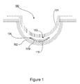
- the interface may be formed by piece 320 and space 350
- theta 1 may be the angle that the incident ray makes with a surface normal at the interface.
- Theta 2 may be the modeled angle that the ray makes with a surface normal as it leaves the interface.
- n 2 may represent the index of refraction of the space 350 and n 1 may represent the index of refraction of the piece 320.
- n 1 is not equal to n 2 then the angles theta 1 and theta 2 will be different as well.
- the electrically variable index of refraction of the liquid crystal layer in space 350 is changed, the path that a light ray would take at the interface will change as well.
- an ophthalmic lens 400 is shown with an embedded variable optic insert 410.
- the ophthalmic lens 400 may have a front curve surface 401 and a back curve surface 402.
- the insert 410 may have a variable optic portion 403 with a liquid crystal layer 404.
- the insert 410 may have multiple liquid crystal layers 404 and 405. Portions of the insert 410 may overlap with the optical zone of the ophthalmic lens 400.
- variable optic portion 500 that may be inserted into an ophthalmic lens is illustrated with a liquid crystal layer 530.
- the variable optic portion 500 may have a similar diversity of materials and structural relevance as has been discussed in other sections of this specification.
- a transparent electrode 545 may be placed on a first transparent substrate 550.
- the first lens surface 540 may be comprised of a dielectric film, and in some exemplary embodiments, alignment layers which may be placed upon the first transparent electrode 545.
- the shape of the dielectric layer of the first lens surface may form a regionally varied shape in the dielectric thickness as depicted. Such a regionally varied shape may introduce additional focusing power of the lens element above the geometric effects discussed in reference to Figure 3 .
- the shaped layer may be formed by injection molding upon the first transparent electrode 545 substrate 550 combination.
- the first transparent electrode 545 and a second transparent electrode 520 may be shaped in various manners.
- the shaping may result in separate and distinct regions being formed that may have energization applied separately.
- the electrodes may be formed into patterns such as a helix from the center of the lens to the periphery which may apply a variable electric field across the liquid crystal layer 530. In either case, such electrode shaping may be performed in addition to the shaping of dielectric layer upon the electrode or instead of such shaping. The shaping of electrodes in these manners may also introduce additional focusing power of the lens element under operation.
- a liquid crystal layer 530 may be located between the first transparent electrode 545 and a second transparent electrode 520.
- the second transparent electrode 520 may be deposited on a top substrate 510, wherein the device formed from the top substrate 510 to the bottom substrate 550 may contain the variable optic portion 500 of the ophthalmic lens.
- Two alignment layers may also be located at 540 and 525 upon the dielectric layer and may surround the liquid crystal layer 530. The alignment layers at 540 and 525 may function to define a resting orientation of the ophthalmic lens.
- the transparent electrode layers 520 and 545 may be in electrical communication with liquid crystal layer 530 and cause a shift in orientation from the resting orientation to at least one energized orientation.
- variable optic insert 600 that may be inserted into an ophthalmic lens is illustrated with two liquid crystal layers 620 and 640.
- Each of the aspects of the various layers around the liquid crystal region may have similar diversity as described in relation to the variable optic insert 500 in Figure 5 .
- the alignment layers may introduce polarization sensitivity into the function of a single liquid crystal element.
- a combination may be formed which may allow for an electrically variable focal characteristic of a lens that is not sensitive to the polarization aspects of incident light upon it.
- a combination of two electrically active liquid crystal layers of the various types and diversity associated with the example at 500 may be formed utilizing three substrate layers.
- the device may be formed by the combination of four different substrates.
- the intermediate substrate 630 may be split into two layers. If the substrates are combined at a later time, a device that functions similarly to item 600 may result.
- the combination of four layers may present a convenient example for the manufacturing of the element where similar devices may be constructed around both 620 and 640 liquid crystal layers where the processing difference may relate to the portion of steps that define alignment features for the liquid crystal element.
- the lens element around a single liquid crystal layer such that is depicted at 500 is spherically symmetric or symmetric upon a rotation of ninety degrees
- two pieces may be assembled into a structure of the type depicted at 600 by rotating the two pieces ninety degrees relative to each other before assembling.
- FIG. 6B An alternative exemplary embodiment which is not sensitive to the polarization aspects of incident light upon it may be found in reference to Figure 6B at item 660.
- a single optical element of the type referred to in discussions relating to Figure 5 may be found with first and second insert pieces at 610 and 630 respectively surrounding an active liquid crystal later comprising liquid crystal elements at 620.
- the aligned liquid crystal elements may act differently upon the different polarization components of incident light.
- a polarizing filter layer may be located at item 665 in Figure 6B .
- the polarizing filter may allow the polarized light consistent with the alignment of item 620 to pass through it while blocking the orthogonal polarization component. Therefore, the electrically active focal aspects of the liquid crystal layer 620 may create a single effect on incident light upon the lens; albeit for one polarization component of the incident light.
- the embodiment of 660 in Figure 6B depicts a polarizing filter at 665, which in some embodiments may be static or in other embodiments may be electrically active.
- This layer may, in an exemplary manner, be located between two insert pieces for containment.
- Such an exemplary embodiment may be found in Figure 6B as the polarization element 665 may be located between a second insert piece 630 and a third insert piece 650.
- both the liquid crystal layer 620 and an associated polarization element 665 may together be located between a first and second insert piece for example.
- a different class of devices may result from forming an ophthalmic device with liquid crystal layers.
- the property that a single layer of aligned liquid crystal layers reacts differently for different polarization components of incident light was exploited in different manners to create devices that deliver a single optical or focal aspect of light to a user's retina.
- the fact that a single aligned layer of liquid crystal material acts on different polarization components of incident light in a different manner defines part of the ophthalmic device function.
- Such a device may be characterized to be a type of bifocal ophthalmic device comprising single polarization sensitive liquid crystal layers.
- An ophthalmic lens of the type described in Figure 4 , 400 may be provided with an insert 500 comprising a liquid crystal layer.
- the layer of the various types that have been described may be aligned by alignment layers and therefore have a sensitivity to a particular polarization state. If the device has a focal adjusting function and has a single aligned liquid crystal layer, or alternatively is a dual layer device, where one liquid crystal layer is aligned in an orthogonal direction to the other liquid crystal layer, and one of the liquid crystal layers is electrically energized to a different level than the other, then the light 670 incident upon the ophthalmic lens 400 may be resolved into two different focal characteristics for each of the polarization directions. As depicted, one of the polarization components 681 may be focused on a path 680 towards a focal point 682 whereas the other polarization component 691 may be focused on a path 690 towards focal point 692.
- ophthalmic devices there are a class of bifocal devices that simultaneously present multiply focused images to a user's eye.
- a human's brain may have a capability of sorting out the two images and perceiving the different images.
- the device at Figure 6C may deliver such a bifocal capability in a superior manner.
- a liquid crystal layer of the type depicted at Figure 6C may divide the light 670 into two polarization components 681 and 691 across the entire visible window. As long as the incident light 670 does not have a polarization preference then the images should appear similarly as would be the case with either focal characteristic alone.
- such an ophthalmic device may be paired with light sources that are projected with defined polarizations for different effects such as displaying information with a select polarization so that it is brought to the magnified image.
- Liquid Crystal Displays may inherently provide such an ambient condition since light may emerge from such a display with a defined polarization characteristic. There may be many embodiments that result from the ability to leverage the devices with multiple focal characteristics.
- the ability to actively control the focus of the device may allow for devices with a range of bifocal conditions.
- a resting state or non-energized state may comprise a bifocal with one polarization unfocused and the other polarization focused on mid distances.
- the mid-distance component may be further focused to near imaging if the lens is bistable, or a range of focal lengths in other embodiments.
- the bifocal characteristic may allow a user to perceive his distance environment simultaneously with a focused image at various distances, which may have advantages of various kinds.
- Microinjection molding embodiments may include, for example, a poly(4-methylpent-1-ene) copolymer resin are used to form lenses with a diameter of between about 6mm to 10mm and a front surface radius of between about 6 mm and 10 mm and a rear surface radius of between about 6 mm and 10 mm and a center thickness of between about 0.050 mm and 1.0 mm.
- Some exemplary embodiments include an insert with diameter of about 8.9 mm and a front surface radius of about 7.9 mm and a rear surface radius of about 7.8 mm and a center thickness of about 0.200 mm and an edge profile of about 0.050 mm radius.
- variable optic insert 104 of Figure 1 may be placed in a mold part 101 and 102 utilized to form an ophthalmic lens in Figure 1 .
- Mold part 101 and 102 material may include, for example, a polyolefin of one or more of: polypropylene, polystyrene, polyethylene, polymethyl methacrylate, and modified polyolefins.
- Other molds may include a ceramic or metallic material.
- a preferred alicyclic co-polymer contains two different alicyclic polymers.
- Various grades of alicyclic co-polymers may have glass transition temperatures ranging from 105°C to 160°C.
- the molds of the invention may include polymers such as polypropylene, polyethylene, polystyrene, polymethyl methacrylate, modified polyolefins containing an alicyclic moiety in the main chain and cyclic polyolefins.
- This blend may be used on either or both mold halves, where it is preferred that this blend is used on the back curve and the front curve consists of the alicyclic co-polymers.
- molds 100 injection molding is utilized according to known techniques; however, embodiments may also include molds fashioned by other techniques including, for example: lathing, diamond turning, or laser cutting.
- lenses are formed on at least one surface of both mold parts 101 and 102.
- one surface of a lens may be formed from a mold part 101 or 102 and another surface of a lens may be formed using a lathing method, or other methods.
- a preferred lens material includes a silicone containing component.
- a "silicone-containing component” is one that contains at least one [-Si-O-] unit in a monomer, macromer or prepolymer.
- the total Si and attached O are present in the silicone-containing component in an amount greater than about 20 weight percent, and more preferably greater than 30 weight percent of the total molecular weight of the silicone-containing component.
- Useful silicone-containing components preferably comprise polymerizable functional groups such as acrylate, methacrylate, acrylamide, methacrylamide, vinyl, N-vinyl lactam, N-vinylamide, and styryl functional groups.
- the ophthalmic lens skirt also called an insert-encapsulating layer, that surrounds the insert may be comprised of standard hydrogel ophthalmic lens formulations.
- Exemplary materials with characteristics that may provide an acceptable match to numerous insert materials may include the Narafilcon family(including Narafilcon A and Narafilcon B), and the Etafilcon family(including Etafilcon A).
- Narafilcon family including Narafilcon A and Narafilcon B
- a more technically inclusive discussion follows on the nature of materials consistent with the art herein. One ordinarily skilled in the art may recognize that other material other than those discussed may also form an acceptable enclosure or partial enclosure of the sealed and encapsulated inserts and should be considered consistent and included within the scope of the claims.
- Suitable silicone containing components include compounds of Formula I where
- “monovalent reactive groups” are groups that can undergo free radical and/or cationic polymerization.
- free radical reactive groups include (meth)acrylates, styryls, vinyls, vinyl ethers, C 1-6 alkyl(meth)acrylates, (meth)acrylamides, C 1-6 alkyl(meth)acrylamides, N-vinyllactams, N-vinylamides, C 2-12 alkenyls, C 2-10 alkenylphenyls, C 2-12 alkenylnaphthyls, C 2-6 alkenylphenylC 1-6 alkyls, O-vinylcarbamates and O-vinylcarbonates.
- Non-limiting examples of cationic reactive groups include vinyl ethers or epoxide groups and mixtures thereof.
- the free radical reactive groups comprises (meth)acrylate, acryloxy, (meth)acrylamide, and mixtures thereof.
- Suitable monovalent alkyl and aryl groups include unsubstituted monovalent C 1 to C 16 alkyl groups, C 6 -C 14 aryl groups, such as substituted and unsubstituted methyl, ethyl, propyl, butyl, 2-hydroxypropyl, propoxypropyl, polyethyleneoxypropyl, combinations thereof and the like.
- b is zero, one R 1 is a monovalent reactive group, and at least 3 R 1 are selected from monovalent alkyl groups having one to 16 carbon atoms, and in another exemplary embodiment from monovalent alkyl groups having one to 6 carbon atoms.
- Non-limiting examples of silicone components of this exemplary embodiment include 2-methyl-,2-hydroxy-3-[3-[1,3,3,3-tetramethyl-1-[(trimethylsilyl)oxy]disiloxanyl]propoxy]propyl ester ("SiGMA”), 2-hydroxy-3-methacryloxypropyloxypropyl-tris(trimethylsiloxy)silane, 3-methacryloxypropyltris(trimethylsiloxy)silane (“TRIS”), 3-methacryloxypropylbis(trimethylsiloxy)methylsilane and 3-methacryloxypropylpentamethyl disiloxane.
- SiGMA 2-methyl-,2-hydroxy-3-[3-[1,3,3,3-tetramethyl-1-[(trimethylsilyl)oxy]disiloxanyl]propoxy]propyl ester
- SiGMA 2-hydroxy-3-methacryloxypropyloxypropyl-tris(trimethylsiloxy)silane
- TMS 3-meth
- b is 2 to 20, 3 to 15 or in some embodiments 3 to 10; at least one terminal R 1 comprises a monovalent reactive group and the remaining R 1 are selected from monovalent alkyl groups having 1 to 16 carbon atoms, and in another embodiment from monovalent alkyl groups having 1 to 6 carbon atoms.
- b is 3 to 15, one terminal R 1 comprises a monovalent reactive group, the other terminal R 1 comprises a monovalent alkyl group having 1 to 6 carbon atoms and the remaining R 1 comprise monovalent alkyl group having 1 to 3 carbon atoms.
- Non-limiting examples of silicone components of this embodiment include (mono-(2-hydroxy-3-methacryloxypropyl)-propyl ether terminated polydimethylsiloxane (400-1000 MW)) (“OH-mPDMS”), monomethacryloxypropyl terminated mono-n-butyl terminated polydimethylsiloxanes (800-1000 MW), (“mPDMS”).
- b is 5 to 400 or from 10 to 300
- both terminal R 1 comprise monovalent reactive groups and the remaining R 1 are independently selected from monovalent alkyl groups having 1 to 18 carbon atoms, which may have ether linkages between carbon atoms and may further comprise halogen.
- the lens of the present invention will be made from a reactive mixture comprising at least about 20 and preferably between about 20 and 70%wt silicone containing components based on total weight of reactive monomer components from which the polymer is made.
- one to four R 1 comprises a vinyl carbonate or carbamate of the formula:
- the silicone-containing vinyl carbonate or vinyl carbamate monomers specifically include: 1,3-bis[4-(vinyloxycarbonyloxy)but-1-yl]tetramethyl-disiloxane; 3-(vinyloxycarbonylthio) propyl-[tris (trimethylsiloxy)silane]; 3-[tris(trimethylsiloxy)silyl] propyl allyl carbamate; 3-[tris(trimethylsiloxy)silyl] propyl vinyl carbamate; trimethylsilylethyl vinyl carbonate; trimethylsilylmethyl vinyl carbonate, and
- R 1 shall comprise a monovalent reactive group and no more than two of the remaining R 1 groups will comprise monovalent siloxane groups.
- silicone-containing components includes polyurethane macromers of the following formulae: Formulae IV-VI (*D*A*D*G) a *D*D*E 1 ; E(*D*G*D*A) a *D*G*D*E 1 or; E(*D*A*D*G) a *D*A*D*E 1 wherein:
- a preferred silicone-containing component is a polyurethane macromer represented by Formula IX, wherein R 16 is a diradical of a diisocyanate after removal of the isocyanate group, such as the diradical of isophorone diisocyanate.
- Another suitable silicone containing macromer is compound of formula X (in which x + y is a number in the range of 10 to 30) formed by the reaction of fluoroether, hydroxy-terminated polydimethylsiloxane, isophorone diisocyanate and isocyanatoethylmethacrylate.
- silicone containing components suitable for use in this invention include macromers containing polysiloxane, polyalkylene ether, diisocyanate, polyfluorinated hydrocarbon, polyfluorinated ether and polysaccharide groups; polysiloxanes with a polar fluorinated graft or side group having a hydrogen atom attached to a terminal difluoro-substituted carbon atom; hydrophilic siloxanyl methacrylates containing ether and siloxanyl linkanges and crosslinkable monomers containing polyether and polysiloxanyl groups. Any of the foregoing polysiloxanes may also be used as the silicone containing component in this invention.
- liquid crystal materials with favorable toxicity may be preferred and naturally derived cholesteryl based liquid crystal materials may be useful.
- the encapsulation technology and materials of ophthalmic inserts may allow a broad choice of materials that may include the LCD display related materials which may typically be of the broad categories related to nematic or cholesteric N or smectic liquid crystals or liquid crystal mixtures.
- Commercially available mixtures such as Merck Specialty chemicals Licristal mixtures for TN, VA, PSVA, IPS and FFS applications and other commercially available mixtures may form a material choice to form a liquid crystal layer.
- mixtures or formulations may contain the following liquid crystal materials: 1-(trans-4-Hexylcyclohexyl)-4-isothiocyanatobenzene liquid crystal, benzoic acid compounds including (4-Octylbenzoic acid and 4-Hexylbenzoic acid), carbonitrile compounds including(4'-Pentyl-4-biphenylcarbonitrile, 4'-Octyl-4-biphenylcarbonitrile, 4'-(Octyloxy)-4-biphenylcarbonitrile, 4'-(Hexyloxy)-4-biphenylcarbonitrile, 4-(trans-4-Pentylcyclohexyl)benzonitrile, 4'-(Pentyloxy)-4-biphenylcarbonitrile, 4'-Hexyl-4-biphenylcarbonitrile), and 4,4'-Azoxyanisole.
- benzoic acid compounds including (4-Octylbenzoic acid and 4-Hexyl
- formulations showing particularly high birefringence of n par - n perp > 0.3 at room temperature may be used as a liquid crystal layer forming material.
- W1825 may be as available from AWAT and BEAM Engineering for Advanced Measurements Co. (BEAMCO).
- ferroelectric liquid crystals may provide function for electric field oriented liquid crystal embodiments, but may also introduce other effects such as magnetic field interactions. Interactions of electromagnetic radiation with the materials may also differ.
- the liquid crystal layers within ophthalmic lenses may need to be aligned in various manners at insert boundaries.
- the alignment for example, may be parallel or perpendicular to the boundaries of the inserts, and this alignment may be obtained by proper processing of the various surfaces.
- the processing may involve coating the substrates of the inserts that contain the liquid crystal (LC) by alignment layers. Those alignment layers are described herein.
- a technique commonly practiced in liquid crystal based devices of various types may be the rubbing technique. This technique may be adapted to account for the curved surfaces such as the ones of the insert pieces used for enclosing the liquid crystal.
- the surfaces may be coated by a polyvinyl alcohol (PVA) layer.
- PVA polyvinyl alcohol
- a PVA layer may be spin coated using a 1 wt.% aqueous solution. The solution may be applied with spin coating at 1000 rpm for time such as approximately 60 s, and then dried. Subsequently, the dried layer may then be rubbed by a soft cloth. In a non-limiting example, the soft cloth may be velvet.
- Photo-alignment may be another technique for producing alignment layers upon liquid crystal enclosures.
- photo-alignment may be desirable due to its non-contact nature and the capability of large scale fabrication.
- the photo-alignment layer used in the liquid crystal variable optic portion may be comprised of a dichroic azobenzene dye (azo dye) capable of aligning predominantly in the direction perpendicular to the polarization of linear polarized light of typically UV wavelengths.
- azo dye dichroic azobenzene dye
- PAAD series azobenzene dyes may be spin coated from a 1 wt.% solution in DMF at 3000 rpm for 30 s. Subsequently, the obtained layer may be exposed to a linear polarized light beam of a UV wavelength (such as for example, 325 nm, 351 nm, 365 nm) or even a visible wavelength (400-500 nm).
- the source of the light may take various forms. In some exemplary embodiments, light may originate from laser sources for example. Other light sources, such as LEDs, halogen and incandescent sources may be other non-limiting examples.
- the light may be collimated in various manners such as through the use of optical lensing devices.
- Light from a laser source may inherently have a degree of collimation, for example.
- photoanisotropic materials are known currently, based on azobenzene polymers, polyesthers, photo-crosslinkable polymer liquid crystals with mesogenic 4-(4-methoxycinnamoyloxy)biphenyl side groups and the like.
- examples of such materials include sulfonic bisazodye SD1 and other azobenzene dyes, particularly, PAAD-series materials available from BEAM Engineering for Advanced Measurements Co. (BEAMCO), Poly(vinyl cinnamates), and others.
- azobenzene dyes for example, Methyl Red
- Some azobenzene dyes may be used for photoalignment by directly doping a liquid crystal layer. Exposure of the azobenzene dye to a polarized light may cause diffusion and adhesion of the azo dyes to and within the bulk of the liquid crystal layer to the boundary layers creating desired alignment conditions.
- Azobenzene dyes such as Methyl Red may also be used in combination with a polymer, for example, PVA.
- a polymer for example, PVA.
- Other photoanisotropic materials capable of enforcing alignment of adjacent layers of liquid crystals may be acceptable are known currently. These examples may include materials based on coumarines, polyesthers, photo-crosslinkable polymer liquid crystals with mesogenic 4-(4-methoxycinnamoyloxy) - biphenyl side groups, Poly(vinyl cinnamates), and others.
- the photo-alignment technology may be advantageous for embodiments comprising patterned orientation of liquid crystal.
- the alignment layer may be obtained by vacuum deposition of silicon oxide on the insert piece substrates.
- SiO 2 may be deposited at low pressure such as ⁇ 10 -6 mbar. It may be possible to provide alignment features at a nanoscaled size that are injection molded into with the creation of the front and back insert pieces. These molded features may be coated in various manners with the materials that have been mentioned or other materials that may directly interact with physical alignment features and transmit the alignment patterning into alignment orientation of liquid crystal molecules.
- Ion beam alignment may be another technique for producing alignment layers upon liquid crystal enclosures.
- collimated argon ion or focused gallium ion beam may be bombarded upon the alignment layer at a defined angle/orientation.
- This type of alignment may also be used to align silicon oxide, diamondlike-carbon (DLC), polyimide and other alignment materials.
- Still further exemplary embodiments may relate to the creation of physical alignment features to the insert pieces after they are formed. Rubbing techniques as are common in other liquid crystal based art may be performed upon the molded surfaces to create physical grooves. The surfaces may also be subjected to a post molding embossing process to create small grooved features upon them. Still further exemplary embodiments may derive from the use of etching techniques which may involve optical patterning processes of various kinds.
- Dielectric films and dielectrics are described herein.
- the dielectric film or dielectrics used in the liquid crystal variable optic portion possess characteristics appropriate to the invention described herein.
- a dielectric may comprise one or more material layers functioning alone or together as a dielectric. Multiple layers may be used to achieve dielectric performance superior to that of a single dielectric.
- the dielectric may permit a defect-free insulating layer at a thickness desired for the discretely variable optic portion, for example, between 1 and 10 ⁇ m.
- a defect may be referred to as a pinhole, as is known by those skilled in the art to be a hole in the dielectric permitting electrical and/or chemical contact through the dielectric.
- the dielectric, at a given thickness, may meet requirements for breakdown voltage, for example, that the dielectric should withstand 100 volts or more.
- the dielectric may allow for fabrication onto curved, conical, spherical, and complex three-dimensional surfaces (e.g., curved surfaces or non-planar surfaces). Typical methods of dip- and spin-coating may be used, or other methods may be employed.
- the dielectric may resist damage from chemicals in the variable optic portion, for example, the liquid crystal or liquid crystal mixture, solvents, acids, and bases or other materials that may be present in the formation of the liquid crystal region.
- the dielectric may resist damage from infrared, ultraviolet, and visible light. Undesirable damage may include degradation to parameters described herein, for example, breakdown voltage and optical transmission.
- the dielectric may resist permeation of ions.
- the dielectric may adhere to an underlying electrode and/or substrate, for example, with the use of an adhesion promotion layer.
- the dielectric may be fabricated using a process which allows for low contamination, low surface defects, conformal coating, and low surface roughness.
- the dielectric may possess relative permittivity or a dielectric constant which is compatible with electrical operation of the system, for example, a low relative permittivity to reduce capacitance for a given electrode area.
- the dielectric may possess high resistivity, thereby permitting a very small current to flow even with high applied voltage.
- the dielectric may possess qualities desired for an optic device, for example, high transmission, low dispersion, and refractive index within a certain range.
- Example, non-limiting, dielectric materials include one or more of Parylene-C, Parylene-HT, Silicon Dioxide, Silicon Nitride, and Teflon AF.
- Electrodes are described herein for applying an electric potential for achieving an electric field across the liquid crystal region.
- An electrode generally comprises one or more material layers functioning alone or together as an electrode.
- the electrode may adhere to an underlying substrate, dielectric coating, or other objects in the system, perhaps with the use of an adhesion promoter (e.g., methacryloxypropyltrimethoxysilane).
- the electrode may form a beneficial native oxide or be processed to create a beneficial oxide layer.
- the electrode may be transparent, substantially transparent or opaque, with high optical transmission and little reflection.
- the electrode may be patterned or etched with known processing methods. For example, the electrodes may be evaporated, sputtered, or electroplated, using photolithographic patterning and/or lift-off processes.
- the electrode may be designed to have suitable resistivity for use in the electrical system described herein, for example, meeting the requirements for resistance in a given geometric construct.
- the electrodes may be manufactured from one or more of indium tin oxide (ITO), aluminum doped zinc oxide (AZO), gold, stainless steel, chrome, graphene, graphene doped layers and aluminum. It will be appreciated that this is not an exhaustive list.
- ITO indium tin oxide
- AZO aluminum doped zinc oxide
- gold gold
- stainless steel chrome
- graphene graphene doped layers and aluminum. It will be appreciated that this is not an exhaustive list.
- a flowchart illustrates exemplary steps that may be used to implement the present invention.
- a first substrate layer which may comprise a back curve surface and have a top surface with a shape of a first type that may differ from the shape of surface of other substrate layers. In some exemplary embodiments, the difference may include a different radius of curvature of the surface at least in a portion that may reside in the optical zone.
- a second substrate layer which may comprise a front curve surface or an intermediate surface or a portion of an intermediate surface for more complicated devices.
- an electrode layer may be deposited upon the first substrate layer. The deposition may occur, for example, by vapor deposition or electroplating.
- the first substrate layer may be part of an insert that has regions both in the optical zone and regions in the non-optic zone.
- the electrode deposition process may simultaneously define interconnect features in some exemplary embodiments.
- a dielectric layer may be formed upon the interconnects or electrodes.
- the dielectric layer may comprise numerous insulating and dielectric layers such as for example silicon dioxide.
- the first substrate layer may be further processed to add an alignment layer upon the previously deposited electrode layer.
- the alignment layer may be deposited upon the top layer on the substrate and then processed in standard manners, for example, rubbing techniques, to create the grooving features that are characteristic of standard alignment layers or by treatment with exposure to energetic particles or light.
- Thin layers of photoanisotropic materials may be processed with light exposure to form alignment layers with various characteristics.
- the second substrate layer may be further processed.
- An electrode layer may be deposited upon the second substrate layer in an analogous fashion to step 703.
- a dielectric layer may be applied upon the second substrate layer upon the electrode layer.
- the dielectric layer may be formed to have a variable thickness across its surface.
- the dielectric layer may be molded upon the first substrate layer.
- a previously formed dielectric layer may be adhered upon the electrode surface of the second substrate piece.
- an alignment layer may be formed upon the second substrate layer in similar fashion to the processing step at 704.
- two separate substrate layers that may form at least a portion of an ophthalmic lens insert may be ready to be joined.
- the two pieces will be brought in close proximity to each other and then liquid crystal material may be filled in between the pieces.
- There may be numerous manners to fill the liquid crystal in between the pieces including as non-limiting examples, vacuum based filling where the cavity is evacuated and liquid crystal material is subsequently allowed to flow into the evacuated space.
- the capillary forces that are present in the space between the lens insert pieces may aid in the filling of the space with liquid crystal material.
- the two pieces may be brought adjacent to each other and then sealed to form a variable optic element with liquid crystal.
- There may be numerous manners of sealing the pieces together including the use of adhesives, sealants, and physical sealing components such as o-rings and snap lock features as non-limiting examples.
- two pieces of the type formed at 709 may be created by repeating method steps 701 to 709 wherein the alignment layers are offset from each other to allow for a lens that may adjust the focal power of non-polarized light.
- the two variable optic layers may be combined to form a single variable optic insert.
- the variable optic portion may be connected to the energy source and intermediate or attached components may be placed thereon.
- variable optic insert resulting at step 710 may be placed within a mold part.
- the variable optic insert may or may not also contain one or more components.
- the variable optic insert is placed in the mold part via mechanical placement.
- Mechanical placement may include, for example, a robot or other automation, such as that known in the industry to place surface mount components.
- Human placement of a variable optic insert is also within the scope of the present invention. Accordingly, any mechanical placement or automation may be utilized which is effective to place a variable optic insert with an energy source within a cast mold part such that the polymerization of a reactive mixture contained by the mold part will include the variable optic in a resultant ophthalmic lens.
- a variable optic insert is placed in a mold part attached to a substrate.
- An energy source and one or more components are also attached to the substrate and are in electrical communication with the variable optic insert.
- Components may include, for example, circuitry to control power applied to the variable optic insert.
- a component includes control mechanism for actuating the variable optic insert to change one or more optical characteristics, such as, for example, a change of state between a first optical power and a second optical power.
- a processor device MEMS, NEMS or other component may also be placed into the variable optic insert and in electrical contact with the energy source.
- a reactive monomer mixture may be deposited into a mold part.
- the variable optic insert may be positioned into contact with the reactive mixture. In some exemplary embodiments the order of placement of variable optic and depositing of monomer mixture may be reversed.
- the first mold part is placed proximate to a second mold part to form a lens-forming cavity with at least some of the reactive monomer mixture and the variable optic insert in the cavity.
- preferred embodiments include an energy source and one or more components also within the cavity and in electrical communication with the variable optic insert.
- the reactive monomer mixture within the cavity is polymerized. Polymerization may be accomplished, for example, via exposure to one or both of actinic radiation and heat.
- the ophthalmic lens is removed from the mold parts with the variable optic insert adhered to or encapsulated within the insert-encapsulating polymerized material making up the ophthalmic lens.
- the lenses of the present invention are soft contact lenses having water contents of about 0 to about 90 percent. More preferably, the lenses are made of monomers containing hydroxy groups, carboxyl groups, or both or be made from silicone-containing polymers, such as siloxanes, hydrogels, silicone hydrogels, and combinations thereof. Material useful for forming the lenses of the invention may be made by reacting blends of macromers, monomers, and combinations thereof along with additives such as polymerization initiators. Suitable materials include, silicone hydrogels made from silicone macromers and hydrophilic monomers.
- automated apparatus 810 is illustrated with one or more transfer interfaces 811.
- Multiple mold parts, each with an associated variable optic insert 814 are contained on a pallet 813 and presented to transfer interfaces 811.
- Exemplary embodiments may include, for example, a single interface individually placing variable optic insert 814, or multiple interfaces (not shown) simultaneously placing variable optic inserts 814 into the multiple mold parts, and in some embodiments, in each mold part. Placement may occur via vertical movement 815 of the transfer interfaces 811.
- variable optic insert 814 includes apparatus to support the variable optic insert 814 while the body of the ophthalmic lens is molded around these components.
- the variable optic insert 814 and an energy source may affixed to holding points in a lens mold (not illustrated).
- the holding points may be affixed with polymerized material of the same type that will be formed into the lens body.
- Other exemplary embodiments include a layer of prepolymer within the mold part onto which the variable optic insert 814 and an energy source may be affixed.
- the controller 900 includes a processor 910, which may include one or more processor components coupled to a communication device 920.
- a controller 900 may be used to transmit energy to the energy source placed in the ophthalmic lens.
- the controller may include one or more processors, coupled to a communication device configured to communicate energy via a communication channel.
- the communication device may be used to electronically control one or more of the placement of a variable optic insert into the ophthalmic lens or the transfer of a command to operate a variable optic device.
- the communication device 920 may also be used to communicate, for example, with one or more controller apparatus or manufacturing equipment components.
- the processor 910 is also in communication with a storage device 930.
- the storage device 930 may comprise any appropriate information storage device, including combinations of magnetic storage devices (e.g., magnetic tape and hard disk drives), optical storage devices, and/or semiconductor memory devices such as Random Access Memory (RAM) devices and Read Only Memory (ROM) devices.
- RAM Random Access Memory
- ROM Read Only Memory
- the storage device 930 may store a program 940 for controlling the processor 910.
- the processor 910 performs instructions of the program 940, and thereby operates in accordance with the present invention.
- the processor 910 may receive information descriptive of variable optic insert placement, processing device placement, and the like.
- the storage device 930 may also store ophthalmic related data in one or more databases 950, 960.
- the database 950 and 960 may include specific control logic for controlling energy to and from a variable optic lens.
- liquid crystal molecules may be of a scale to be impossibly small to depict against the scale of insert pieces.
- the depiction of features that represent liquid crystal molecules at a similar scale to insert pieces to allow for representation of factors such as the alignment of the molecules is therefore such an example of a depicted scale that in actual embodiments may assume much different relative scale.
Landscapes
- Ophthalmology & Optometry (AREA)
- Health & Medical Sciences (AREA)
- Physics & Mathematics (AREA)
- Optics & Photonics (AREA)
- General Health & Medical Sciences (AREA)
- General Physics & Mathematics (AREA)
- Engineering & Computer Science (AREA)
- Manufacturing & Machinery (AREA)
- Mechanical Engineering (AREA)
- Microelectronics & Electronic Packaging (AREA)
- Liquid Crystal (AREA)
- Eyeglasses (AREA)
- Prostheses (AREA)
Applications Claiming Priority (2)
| Application Number | Priority Date | Filing Date | Title |
|---|---|---|---|
| US201361878723P | 2013-09-17 | 2013-09-17 | |
| US14/172,142 US20150077658A1 (en) | 2013-09-17 | 2014-02-04 | Variable optic ophthalmic device including shaped liquid crystal elements and polarizing elements |
Publications (2)
| Publication Number | Publication Date |
|---|---|
| EP2848982A2 true EP2848982A2 (fr) | 2015-03-18 |
| EP2848982A3 EP2848982A3 (fr) | 2015-04-08 |
Family
ID=51541029
Family Applications (1)
| Application Number | Title | Priority Date | Filing Date |
|---|---|---|---|
| EP14185167.5A Withdrawn EP2848982A3 (fr) | 2013-09-17 | 2014-09-17 | Dispositif ophtalmique à optique variable comprenant des éléments à cristaux liquides et des éléments polarisants |
Country Status (13)
| Country | Link |
|---|---|
| US (1) | US20150077658A1 (fr) |
| EP (1) | EP2848982A3 (fr) |
| JP (1) | JP2015060225A (fr) |
| KR (1) | KR20150032231A (fr) |
| CN (1) | CN104460036A (fr) |
| AU (1) | AU2014221207B2 (fr) |
| BR (1) | BR102014023065A2 (fr) |
| CA (1) | CA2863385A1 (fr) |
| HK (2) | HK1204495A1 (fr) |
| IL (1) | IL234420A0 (fr) |
| RU (1) | RU2594437C2 (fr) |
| SG (1) | SG10201405453RA (fr) |
| TW (1) | TWI649073B (fr) |
Cited By (2)
| Publication number | Priority date | Publication date | Assignee | Title |
|---|---|---|---|---|
| US10859868B2 (en) | 2017-08-11 | 2020-12-08 | Coopervision International Limited | Flexible liquid crystal cells and lenses |
| US11003016B2 (en) | 2018-09-21 | 2021-05-11 | Coopervision International Limited | Flexible, adjustable lens power liquid crystal cells and lenses |
Families Citing this family (28)
| Publication number | Priority date | Publication date | Assignee | Title |
|---|---|---|---|---|
| US9475709B2 (en) | 2010-08-25 | 2016-10-25 | Lockheed Martin Corporation | Perforated graphene deionization or desalination |
| US9610546B2 (en) | 2014-03-12 | 2017-04-04 | Lockheed Martin Corporation | Separation membranes formed from perforated graphene and methods for use thereof |
| US10118130B2 (en) | 2016-04-14 | 2018-11-06 | Lockheed Martin Corporation | Two-dimensional membrane structures having flow passages |
| US9744617B2 (en) | 2014-01-31 | 2017-08-29 | Lockheed Martin Corporation | Methods for perforating multi-layer graphene through ion bombardment |
| US9834809B2 (en) | 2014-02-28 | 2017-12-05 | Lockheed Martin Corporation | Syringe for obtaining nano-sized materials for selective assays and related methods of use |
| US10653824B2 (en) | 2012-05-25 | 2020-05-19 | Lockheed Martin Corporation | Two-dimensional materials and uses thereof |
| US10418143B2 (en) | 2015-08-05 | 2019-09-17 | Lockheed Martin Corporation | Perforatable sheets of graphene-based material |
| US10696554B2 (en) | 2015-08-06 | 2020-06-30 | Lockheed Martin Corporation | Nanoparticle modification and perforation of graphene |
| US10376845B2 (en) | 2016-04-14 | 2019-08-13 | Lockheed Martin Corporation | Membranes with tunable selectivity |
| US10980919B2 (en) | 2016-04-14 | 2021-04-20 | Lockheed Martin Corporation | Methods for in vivo and in vitro use of graphene and other two-dimensional materials |
| US9592475B2 (en) | 2013-03-12 | 2017-03-14 | Lockheed Martin Corporation | Method for forming perforated graphene with uniform aperture size |
| US9572918B2 (en) | 2013-06-21 | 2017-02-21 | Lockheed Martin Corporation | Graphene-based filter for isolating a substance from blood |
| WO2015116857A2 (fr) | 2014-01-31 | 2015-08-06 | Lockheed Martin Corporation | Procédés de formation de structures composites avec un matériau à deux dimensions à l'aide d'une couche de support non-sacrificielle poreuse |
| JP2017510461A (ja) | 2014-01-31 | 2017-04-13 | ロッキード マーティン コーポレイションLockheed Martin Corporation | 広幅イオン場を用いる二次元材料の穿孔 |
| CA2942496A1 (fr) | 2014-03-12 | 2015-09-17 | Lockheed Martin Corporation | Membranes de separation formees a partir de graphene perfore |
| US9841614B2 (en) * | 2014-06-13 | 2017-12-12 | Verily Life Sciences Llc | Flexible conductor for use within a contact lens |
| WO2016036888A1 (fr) | 2014-09-02 | 2016-03-10 | Lockheed Martin Corporation | Membranes d'hémodialyse et d'hémofiltration basées sur un matériau membranaire bidimensionnel et procédés employant ces dernières |
| US10678068B2 (en) * | 2015-12-18 | 2020-06-09 | Verily Life Sciences Llc | Electrochromic contact lens |
| WO2017180141A1 (fr) | 2016-04-14 | 2017-10-19 | Lockheed Martin Corporation | Atténuation interfaciale sélective des défauts du graphène |
| EP3443329A4 (fr) | 2016-04-14 | 2020-04-08 | Lockheed Martin Corporation | Procédés permettant la surveillance et la commande in situ d'une formation ou cicatrisation de défaut |
| JP2019511451A (ja) | 2016-04-14 | 2019-04-25 | ロッキード・マーチン・コーポレーション | 浮遊法を用いてグラフェンシートを大判転写用に処理する方法 |
| US10365504B2 (en) | 2016-09-23 | 2019-07-30 | Verily Life Sciences Llc | Rigid, gas-permeable polymer as over-mold and sealant for adaptive ophthalmic lens |
| KR101886792B1 (ko) | 2017-01-13 | 2018-08-08 | 경북대학교 산학협력단 | 액정상 고분자를 이용한 이중 초점 렌즈 |
| KR101866193B1 (ko) | 2017-01-13 | 2018-06-11 | 경북대학교 산학협력단 | 이중 초점 렌즈 및 그 제조 방법 |
| CN111093958B (zh) | 2017-09-08 | 2022-10-28 | 威里利生命科学有限责任公司 | 湿润环境中的自愈引线 |
| KR101979886B1 (ko) * | 2017-10-11 | 2019-05-17 | 가톨릭대학교 산학협력단 | 다초점 인공 수정체 |
| DE102020209934A1 (de) | 2020-08-06 | 2022-02-10 | Robert Bosch Gesellschaft mit beschränkter Haftung | Herstellungsverfahren für ein mikromechanisches Bauelement, entsprechendes mikromechanisches Bauelement und entsprechende Anordnung |
| KR20250154527A (ko) * | 2020-08-19 | 2025-10-28 | 이-비전 스마트 옵틱스, 아이엔씨. | 전기 활성 스포츠 안경 |
Family Cites Families (15)
| Publication number | Priority date | Publication date | Assignee | Title |
|---|---|---|---|---|
| JPS62169116A (ja) * | 1986-01-21 | 1987-07-25 | Olympus Optical Co Ltd | 可変焦点液晶レンズ |
| JP2581767B2 (ja) * | 1988-07-07 | 1997-02-12 | オリンパス光学工業株式会社 | 可変焦点レンズ系 |
| AU6434594A (en) * | 1993-04-07 | 1994-10-24 | Technology Partnership Plc, The | Switchable lens |
| US6437925B1 (en) * | 1998-06-30 | 2002-08-20 | Olympus Optical Co., Ltd. | Optical apparatus |
| RU2234722C2 (ru) * | 1999-11-11 | 2004-08-20 | Стефен КЕРТИН | Линзы с изменяемым фокусным расстоянием, используемые для очков |
| US8885139B2 (en) * | 2005-01-21 | 2014-11-11 | Johnson & Johnson Vision Care | Adaptive electro-active lens with variable focal length |
| AR064985A1 (es) * | 2007-01-22 | 2009-05-06 | E Vision Llc | Lente electroactivo flexible |
| AR064986A1 (es) * | 2007-01-22 | 2009-05-06 | Pixeloptics Inc | Material cristalino liquido colesterico en lente electroactiva |
| US7926940B2 (en) * | 2007-02-23 | 2011-04-19 | Pixeloptics, Inc. | Advanced electro-active optic device |
| AU2008218240B2 (en) * | 2007-02-23 | 2014-01-30 | E-Vision Smart Optics, Inc. | Ophthalmic dynamic aperture |
| FR2939916B1 (fr) * | 2008-12-15 | 2011-04-01 | Essilor Int | Element optique a puissance variable |
| JP5359829B2 (ja) * | 2009-12-03 | 2013-12-04 | カシオ計算機株式会社 | 液晶レンズと、それを用いた焦点距離可変眼鏡 |
| US20120212696A1 (en) * | 2011-01-27 | 2012-08-23 | Pixeloptics, Inc. | Variable optical element comprising a liquid crystal alignment layer |
| US8827446B2 (en) * | 2011-03-10 | 2014-09-09 | Hpo Assets Llc | Electronic lens comprised of hybrid materials |
| BR112014015418A8 (pt) * | 2011-12-23 | 2017-07-04 | Johnson & Johnson Vision Care | dispositivo oftálmico de óptica variável que inclui elementos de cristal líquido |
-
2014
- 2014-02-04 US US14/172,142 patent/US20150077658A1/en not_active Abandoned
- 2014-09-02 IL IL234420A patent/IL234420A0/en unknown
- 2014-09-03 AU AU2014221207A patent/AU2014221207B2/en not_active Expired - Fee Related
- 2014-09-03 SG SG10201405453RA patent/SG10201405453RA/en unknown
- 2014-09-12 CA CA2863385A patent/CA2863385A1/fr not_active Abandoned
- 2014-09-15 TW TW103131686A patent/TWI649073B/zh not_active IP Right Cessation
- 2014-09-16 RU RU2014137439/14A patent/RU2594437C2/ru not_active IP Right Cessation
- 2014-09-16 JP JP2014187520A patent/JP2015060225A/ja active Pending
- 2014-09-17 KR KR20140123698A patent/KR20150032231A/ko not_active Withdrawn
- 2014-09-17 EP EP14185167.5A patent/EP2848982A3/fr not_active Withdrawn
- 2014-09-17 BR BR102014023065A patent/BR102014023065A2/pt not_active Application Discontinuation
- 2014-09-17 CN CN201410475468.6A patent/CN104460036A/zh active Pending
-
2015
- 2015-05-28 HK HK15105053.6A patent/HK1204495A1/xx unknown
- 2015-09-04 HK HK15108623.1A patent/HK1208082A1/en unknown
Non-Patent Citations (1)
| Title |
|---|
| None |
Cited By (4)
| Publication number | Priority date | Publication date | Assignee | Title |
|---|---|---|---|---|
| US10859868B2 (en) | 2017-08-11 | 2020-12-08 | Coopervision International Limited | Flexible liquid crystal cells and lenses |
| US11860470B2 (en) | 2017-08-11 | 2024-01-02 | Coopervision International Limited | Flexible liquid crystal cells and lenses |
| US11003016B2 (en) | 2018-09-21 | 2021-05-11 | Coopervision International Limited | Flexible, adjustable lens power liquid crystal cells and lenses |
| US11520181B2 (en) | 2018-09-21 | 2022-12-06 | Coopervision International Limited | Flexible, adjustable lens power liquid crystal cells and lenses |
Also Published As
| Publication number | Publication date |
|---|---|
| IL234420A0 (en) | 2014-11-30 |
| TWI649073B (zh) | 2019-02-01 |
| CA2863385A1 (fr) | 2015-03-17 |
| HK1208082A1 (en) | 2016-02-19 |
| TW201531287A (zh) | 2015-08-16 |
| BR102014023065A2 (pt) | 2015-09-15 |
| HK1204495A1 (en) | 2015-11-20 |
| KR20150032231A (ko) | 2015-03-25 |
| SG10201405453RA (en) | 2015-04-29 |
| JP2015060225A (ja) | 2015-03-30 |
| RU2594437C2 (ru) | 2016-08-20 |
| EP2848982A3 (fr) | 2015-04-08 |
| US20150077658A1 (en) | 2015-03-19 |
| AU2014221207B2 (en) | 2019-04-11 |
| AU2014221207A1 (en) | 2015-04-02 |
| RU2014137439A (ru) | 2016-04-10 |
| CN104460036A (zh) | 2015-03-25 |
Similar Documents
| Publication | Publication Date | Title |
|---|---|---|
| AU2014221207B2 (en) | Variable optic ophthalmic device including shaped liquid crystal elements and polarizing elements | |
| EP2848980B1 (fr) | Procédé et appareil pour dispositifs ophtalmiques incorporant des régions de formes spécifiques avec des réseaux de cristaux liquides polymérisés. | |
| US9500882B2 (en) | Variable optic ophthalmic device including shaped liquid crystal elements with nano-scaled droplets of liquid crystal | |
| EP2848986B1 (fr) | Procédé et appareil pour dispositifs ophtalmiques incorporant des diélectriques et des gouttelettes de cristaux liquides nanométriques | |
| EP2848985B1 (fr) | Dispositifs ophtalmiques comprenant des diélectriques et des réseaux de cristaux liquides polymérisés. | |
| US9268154B2 (en) | Method and apparatus for ophthalmic devices including hybrid alignment layers and shaped liquid crystal layers | |
| US20150138454A1 (en) | Variable optic ophthalmic device including liquid crystal elements | |
| EP2851743A1 (fr) | Dispositif ophthalmique avec couche à cristaux liquides à gradient d'indice | |
| EP2848983B1 (fr) | Procédé et appareil pour dispositifs ophtalmiques incorporant des régions de cristaux liquides de formes spécifiques à gradient d'indice | |
| EP3264164A1 (fr) | Procédés de formation de dispositifs ophtalmiques optiques variables comprenant des éléments à cristaux liquides formés | |
| HK1208081B (en) | Method and apparatus for ophthalmic devices including shaped liquid crystal polymer networked regions of liquid crystal | |
| HK1208077B (en) | Method and apparatus for ophthalmic devices comprising dielectrics and nano-scaled droplets of liquid crystal | |
| HK1208083B (en) | Variable optic ophthalmic device including shaped liquid crystal elements with nano-scaled droplets of liquid crystal | |
| HK1208085B (en) | Ophthalmic devices comprising dielectrics and liquid crystal polymer networks | |
| HK1208084B (en) | Method and apparatus for ophthalmic devices including gradient-indexed and shaped liquid crystal layers |
Legal Events
| Date | Code | Title | Description |
|---|---|---|---|
| PUAL | Search report despatched |
Free format text: ORIGINAL CODE: 0009013 |
|
| PUAI | Public reference made under article 153(3) epc to a published international application that has entered the european phase |
Free format text: ORIGINAL CODE: 0009012 |
|
| 17P | Request for examination filed |
Effective date: 20140917 |
|
| AK | Designated contracting states |
Kind code of ref document: A2 Designated state(s): AL AT BE BG CH CY CZ DE DK EE ES FI FR GB GR HR HU IE IS IT LI LT LU LV MC MK MT NL NO PL PT RO RS SE SI SK SM TR |
|
| AX | Request for extension of the european patent |
Extension state: BA ME |
|
| RIN1 | Information on inventor provided before grant (corrected) |
Inventor name: TONER, ADAM Inventor name: TABIRIAN, NELSON V. Inventor name: USKOVA, OLENA Inventor name: FLITSCH, FREDERICK A. Inventor name: PUGH, RANDALL BRAXTON Inventor name: SERAK, SVETLANA Inventor name: DE SIO, LUCIANO Inventor name: RIALL, JAMES DANIEL Inventor name: PANDOJIRAO-S, PRAVEEN |
|
| AK | Designated contracting states |
Kind code of ref document: A3 Designated state(s): AL AT BE BG CH CY CZ DE DK EE ES FI FR GB GR HR HU IE IS IT LI LT LU LV MC MK MT NL NO PL PT RO RS SE SI SK SM TR |
|
| AX | Request for extension of the european patent |
Extension state: BA ME |
|
| RIC1 | Information provided on ipc code assigned before grant |
Ipc: G02C 7/08 20060101ALI20150304BHEP Ipc: G02C 7/04 20060101AFI20150304BHEP |
|
| R17P | Request for examination filed (corrected) |
Effective date: 20151008 |
|
| RBV | Designated contracting states (corrected) |
Designated state(s): AL AT BE BG CH CY CZ DE DK EE ES FI FR GB GR HR HU IE IS IT LI LT LU LV MC MK MT NL NO PL PT RO RS SE SI SK SM TR |
|
| REG | Reference to a national code |
Ref country code: HK Ref legal event code: DE Ref document number: 1208082 Country of ref document: HK |
|
| 17Q | First examination report despatched |
Effective date: 20160224 |
|
| STAA | Information on the status of an ep patent application or granted ep patent |
Free format text: STATUS: THE APPLICATION HAS BEEN WITHDRAWN |
|
| 18W | Application withdrawn |
Effective date: 20190621 |
|
| REG | Reference to a national code |
Ref country code: HK Ref legal event code: WD Ref document number: 1208082 Country of ref document: HK |