EP2851696B1 - Verfahren zur Extraktion von Rekombinationsmerkmalen an metallisierten Halbleiteroberflächen - Google Patents
Verfahren zur Extraktion von Rekombinationsmerkmalen an metallisierten Halbleiteroberflächen Download PDFInfo
- Publication number
- EP2851696B1 EP2851696B1 EP13185659.3A EP13185659A EP2851696B1 EP 2851696 B1 EP2851696 B1 EP 2851696B1 EP 13185659 A EP13185659 A EP 13185659A EP 2851696 B1 EP2851696 B1 EP 2851696B1
- Authority
- EP
- European Patent Office
- Prior art keywords
- recombination
- metal
- metallized
- current density
- saturation current
- Prior art date
- Legal status (The legal status is an assumption and is not a legal conclusion. Google has not performed a legal analysis and makes no representation as to the accuracy of the status listed.)
- Not-in-force
Links
Images


Classifications
-
- G—PHYSICS
- G01—MEASURING; TESTING
- G01R—MEASURING ELECTRIC VARIABLES; MEASURING MAGNETIC VARIABLES
- G01R31/00—Arrangements for testing electric properties; Arrangements for locating electric faults; Arrangements for electrical testing characterised by what is being tested not provided for elsewhere
- G01R31/26—Testing of individual semiconductor devices
- G01R31/265—Contactless testing
- G01R31/2656—Contactless testing using non-ionising electromagnetic radiation, e.g. optical radiation
-
- G—PHYSICS
- G01—MEASURING; TESTING
- G01N—INVESTIGATING OR ANALYSING MATERIALS BY DETERMINING THEIR CHEMICAL OR PHYSICAL PROPERTIES
- G01N21/00—Investigating or analysing materials by the use of optical means, i.e. using sub-millimetre waves, infrared, visible or ultraviolet light
- G01N21/62—Systems in which the material investigated is excited whereby it emits light or causes a change in wavelength of the incident light
- G01N21/63—Systems in which the material investigated is excited whereby it emits light or causes a change in wavelength of the incident light optically excited
-
- G—PHYSICS
- G01—MEASURING; TESTING
- G01N—INVESTIGATING OR ANALYSING MATERIALS BY DETERMINING THEIR CHEMICAL OR PHYSICAL PROPERTIES
- G01N21/00—Investigating or analysing materials by the use of optical means, i.e. using sub-millimetre waves, infrared, visible or ultraviolet light
- G01N21/62—Systems in which the material investigated is excited whereby it emits light or causes a change in wavelength of the incident light
- G01N21/63—Systems in which the material investigated is excited whereby it emits light or causes a change in wavelength of the incident light optically excited
- G01N21/64—Fluorescence; Phosphorescence
- G01N21/6408—Fluorescence; Phosphorescence with measurement of decay time, time resolved fluorescence
-
- G—PHYSICS
- G01—MEASURING; TESTING
- G01N—INVESTIGATING OR ANALYSING MATERIALS BY DETERMINING THEIR CHEMICAL OR PHYSICAL PROPERTIES
- G01N21/00—Investigating or analysing materials by the use of optical means, i.e. using sub-millimetre waves, infrared, visible or ultraviolet light
- G01N21/62—Systems in which the material investigated is excited whereby it emits light or causes a change in wavelength of the incident light
- G01N21/63—Systems in which the material investigated is excited whereby it emits light or causes a change in wavelength of the incident light optically excited
- G01N21/64—Fluorescence; Phosphorescence
- G01N21/6489—Photoluminescence of semiconductors
-
- G—PHYSICS
- G01—MEASURING; TESTING
- G01N—INVESTIGATING OR ANALYSING MATERIALS BY DETERMINING THEIR CHEMICAL OR PHYSICAL PROPERTIES
- G01N33/00—Investigating or analysing materials by specific methods not covered by groups G01N1/00 - G01N31/00
-
- G—PHYSICS
- G01—MEASURING; TESTING
- G01N—INVESTIGATING OR ANALYSING MATERIALS BY DETERMINING THEIR CHEMICAL OR PHYSICAL PROPERTIES
- G01N33/00—Investigating or analysing materials by specific methods not covered by groups G01N1/00 - G01N31/00
- G01N33/0095—Semiconductive materials
-
- H—ELECTRICITY
- H02—GENERATION; CONVERSION OR DISTRIBUTION OF ELECTRIC POWER
- H02S—GENERATION OF ELECTRIC POWER BY CONVERSION OF INFRARED RADIATION, VISIBLE LIGHT OR ULTRAVIOLET LIGHT, e.g. USING PHOTOVOLTAIC [PV] MODULES
- H02S50/00—Monitoring or testing of PV systems, e.g. load balancing or fault identification
-
- H—ELECTRICITY
- H10—SEMICONDUCTOR DEVICES; ELECTRIC SOLID-STATE DEVICES NOT OTHERWISE PROVIDED FOR
- H10P—GENERIC PROCESSES OR APPARATUS FOR THE MANUFACTURE OR TREATMENT OF DEVICES COVERED BY CLASS H10
- H10P74/00—Testing or measuring during manufacture or treatment of wafers, substrates or devices
- H10P74/20—Testing or measuring during manufacture or treatment of wafers, substrates or devices characterised by the properties tested or measured, e.g. structural or electrical properties
- H10P74/207—Electrical properties, e.g. testing or measuring of resistance, deep levels or capacitance-voltage characteristics
-
- H—ELECTRICITY
- H10—SEMICONDUCTOR DEVICES; ELECTRIC SOLID-STATE DEVICES NOT OTHERWISE PROVIDED FOR
- H10P—GENERIC PROCESSES OR APPARATUS FOR THE MANUFACTURE OR TREATMENT OF DEVICES COVERED BY CLASS H10
- H10P74/00—Testing or measuring during manufacture or treatment of wafers, substrates or devices
- H10P74/27—Structural arrangements therefor
- H10P74/277—Circuits for electrically characterising or monitoring manufacturing processes, e.g. circuits in tested chips or circuits in testing wafers
-
- Y—GENERAL TAGGING OF NEW TECHNOLOGICAL DEVELOPMENTS; GENERAL TAGGING OF CROSS-SECTIONAL TECHNOLOGIES SPANNING OVER SEVERAL SECTIONS OF THE IPC; TECHNICAL SUBJECTS COVERED BY FORMER USPC CROSS-REFERENCE ART COLLECTIONS [XRACs] AND DIGESTS
- Y02—TECHNOLOGIES OR APPLICATIONS FOR MITIGATION OR ADAPTATION AGAINST CLIMATE CHANGE
- Y02E—REDUCTION OF GREENHOUSE GAS [GHG] EMISSIONS, RELATED TO ENERGY GENERATION, TRANSMISSION OR DISTRIBUTION
- Y02E10/00—Energy generation through renewable energy sources
- Y02E10/50—Photovoltaic [PV] energy
Definitions
- the present disclosure relates to methods for the extraction of recombination characteristics at metallized semiconductor surfaces and of metallized semiconductor junctions, such as p-n junctions or high/low junctions, based on photo-conductance decay measurements.
- Methods of the present disclosure may for example be used for determining recombination characteristics of passivated emitter or base contacts of photovoltaic cells.
- the metal-silicon interface at the metal contacts provides a highly recombination active surface for minority charge carriers. This results in recombination currents and degradation of the device performance.
- the open-circuit voltage V oc of photovoltaic cells decreases with increasing recombination at the metal contacts. Reduction of recombination currents at metal contacts is considered to be a critical aspect of enhancing efficiencies of highly efficient silicon photovoltaic cells.
- the saturation current density of metallized semiconductor (e.g. silicon) junctions is a measure for the magnitude of the recombination current and thus for the effective surface recombination velocity of the metallized junction.
- Recombination at a metal-emitter interface of e.g. a silicon photovoltaic cell may be determined by extracting the saturation current density of the metallized emitter from J sc -V oc (short circuit current density - open circuit voltage) measurements and from dark current measurements as a function of metal coverage.
- J sc -V oc short circuit current density - open circuit voltage
- dark current measurements as a function of metal coverage.
- Photoluminescence measurements can be done at different stages of the processing and have the advantage of spatial resolution, but obtaining information on the injection level is only possible by using complicated algorithms. This compromises the reliability of saturation currents extracted using such techniques.
- Photo-conductance decay measurements allow for effective lifetime extraction at different injection levels. Such measurements have been used for the determination of the (emitter) saturation current density at high injection levels. When using this approach for the measurement of the saturation current density at a metal/silicon interface, care must be taken to prevent wafer conductivity to be dominated by the metal layer. Therefore a very thin metal layer (e.g. an Al layer with a thickness of about 1 nm) is required to permit a photo-conductance decay measurement on such structures. It is a disadvantage that such thin aluminum layers may be fully oxidized before measurements are done, since aluminum is known to react with oxygen in ambient air to form aluminum oxide. Furthermore, many metallization techniques do not allow the deposition of such thin metal layers.
- a very thin metal layer e.g. an Al layer with a thickness of about 1 nm
- the document WO2013/016469 describes solar metrology methods and an apparatus to measure the photoluminescence of incoming wafers and extract parameters such as minority carrier life time , diffusion length, and defect density that may be used to predict final solar cell efficiency.
- Photo-conductance calibrated photoluminescence imaging has been used for the local determination of saturation current densities of highly doped regions in silicon wafers, as reported by J. Mueller et al in "Reverse saturation current density imaging of highly doped regions in silicon: A photoluminescence approach", Solar Energy Materials & Solar Cells 106 (2012) 76-79 .
- the saturation current density is determined under high injection conditions based on photo-conductance calibrated photoluminescence images acquired at different high injection levels.
- the technique can also be applied to partially metallized samples. Using this measurement method the recombination at metal contacts to highly doped silicon can be quantified.
- the present disclosure aims to provide methods for the extraction of recombination characteristics at metallized semiconductor surfaces from photo-conductance decay measurements, wherein the methods can be used at arbitrary injection levels, i.e. not only at high injection levels but also at low injection levels.
- the present disclosure aims to provide methods for the extraction of recombination characteristics at metallized semiconductor surfaces from photo-conductance decay measurements, wherein the need for using a very thin metal layer is avoided.
- a recombination characteristic can for example comprise a saturation current density, an upper limit or a lower limit of a saturation current density, a surface recombination velocity, an upper limit or a lower limit of a surface recombination velocity or an (inverse) effective lifetime.
- a metallized semiconductor surface may be a semiconductor surface covered by a metal layer wherein the metal layer is in direct physical contact with the semiconductor surface.
- a metallized semiconductor surface may also be a semiconductor surface covered by a stack comprising a thin passivation layer (e.g. having a thickness less than 5 nm) and a metal layer (also referred to as a passivated contact) wherein the passivation layer is sufficiently thin to enable an electrical contact between the semiconductor and the metal, e.g. sufficiently thin to allow a tunnel current passing through the thin passivation layer.
- the stack may comprise a dielectric layer, e.g. silicon oxide layer, and a metal layer.
- the stack may comprise a dielectric layer (e.g. aluminum oxide layer), a poly-silicon layer (e.g. p ++ poly-silicon) and a metal layer (e.g. aluminum layer).
- the stack may comprise an amorphous silicon layer and a metal layer.
- This disclosure is related to methods for the determination of injection dependent recombination characteristics at metallized semiconductor surfaces, such as metallized silicon surfaces, based on effective lifetime measurements as a function of metal contact area coverage.
- the present disclosure is further related to methods for the determination of saturation current densities of metal contacted junctions in high injection based on effective lifetime measurements.
- a method for determining a recombination characteristic at a semiconductor surface comprises: providing a test structure, wherein the test structure comprises a semiconductor substrate having a first surface and a second surface opposite to the first surface, a first passivation layer on the first surface, a second passivation layer on the second surface, the second passivation layer having a plurality of openings at predetermined locations, and a plurality of metal features in (electrical) contact with the second semiconductor surface at the predetermined locations, thus forming metallized surfaces at the predetermined locations and non-metallized outside the predetermined locations, wherein a characteristic size of the metal features is smaller than an effective diffusion length in the underlying semiconductor at the predetermined locations and the metal features being provided with a spacing smaller than an effective diffusion length in the underlying semiconductor outside the predetermined locations, the metal features being grouped in a plurality of zones, each of the plurality of zones having a different metal coverage.
- the method further comprises: performing a photo-conductance decay measurement in each of the plurality of zones, thereby determining effective lifetimes for different injection levels as a function of metal coverage; and extracting the recombination characteristic from the measured effective lifetimes.
- the metal coverage is defined as the ratio between the contacted area (metallized surface area) and the total area of a zone.
- the first passivation layer of the test structure may be a continuous layer covering the first surface.
- the first passivation layer of the test structure may have a plurality of openings at predetermined locations (as for the second passivation layer), and a plurality of metal features in contact with the first semiconductor surface at the predetermined locations. In such embodiments it is preferred to align the plurality of metal features in contact with the first surface to the plurality of metal features in contact with the second surface. It is an advantage of using a continuous first passivation layer covering the first surface that there is no need for performing such alignment.
- extracting the recombination characteristic from the measured effective lifetimes may comprise determining a difference between the recombination characteristic at a metallized surface and the recombination characteristic at a non-metallized surface for each of the injection levels from the slope of a linear fit of inverse effective lifetime versus metal coverage. This difference may be considered as a lower limit for the recombination characteristic at the metallized surface.
- the method may further comprise determining an upper value (estimate) of the recombination characteristic at a non-metallized surface and/or determining a lower value (estimate) of the recombination characteristic at a metallized surface for each of the injection levels from the slope of a linear fit of inverse effective lifetime versus metal coverage.
- Extracting the recombination characteristic in a method of the present disclosure may comprise determining an upper limit of the recombination characteristic at a non-metallized surface from an intercept with the zero metal coverage axis of a linear fit of the inverse effective lifetime versus metal coverage.
- the recombination characteristic may be a surface recombination velocity, an inverse lifetime or a saturation current density.
- the semiconductor substrate of the test structure may comprise a first doped region forming a first p-n junction underlying the first surface and/or a second doped region forming a second p-n junction underlying the second surface.
- the semiconductor substrate of the test structure may comprise a doped region forming a first high-low junction underlying the first surface and/or a second doped region forming a second high-low junction underlying the second surface.
- extracting the recombination characteristic may comprise determining a total saturation current density at high injection for each metal coverage from the slope of inverse effective lifetime versus injection level, performing a correction of the effective lifetimes for Auger recombination, and afterwards extracting the saturation current density at a metallized surface and the saturation current density at a non-metallized surface from the slope of a linear fit of the total saturation current density versus metal coverage.
- the semiconductor substrate may be a silicon substrate, the present disclosure not being limited thereto.
- the method may further comprise correcting the measured injection levels and/or correcting the measured effective lifetimes taking into account the influence of metal conductivity, before extracting the recombination characteristics.
- Methods of the present disclosure may advantageously be used for determining recombination characteristics of (passivated) emitter contacts and/or (passivated) base contacts of photovoltaic cells.
- recombination characteristics may be determined as a function of injection level. This may for example provide an indication on how well contact passivation performs at both low and high illumination intensities.
- the injection level may be measured together with the recombination characteristics, i.e. the injection level may be obtained from the photo-conductance measurement itself. It is an advantage of being able to measure the injection level that accurate recombination characteristics may be extracted.
- the present disclosure provides methods based on photo-conductance decay measurements for the determination of recombination characteristics, such as saturation current densities, recombination currents, surface recombination velocities or effective lifetimes, at a metallized semiconductor surface.
- recombination characteristics are extracted from effective lifetime measurements as a function of metal contact fraction, using a dedicated test structure.
- test structure used in a method of the present disclosure comprises a semiconductor substrate with a predetermined metal pattern on at least one of the semiconductor substrate surfaces.
- the focus is on test structures with a metal pattern on one semiconductor surface, but the present disclosure is not limited thereto and test structures having a metal pattern at both semiconductor surfaces may be used.
- the test structures have a patterned metal layer in contact with the semiconductor, e.g. silicon, surface at predetermined locations, to enable the measurement of recombination characteristics at metal contacts by means of a photo-conductance decay method.
- the test structures allow covering parts of a semiconductor substrate or semiconductor wafer with a thick metal layer, while ensuring that the conductivity of the test structure remains dominated by the conductivity of the semiconductor substrate. As a result, minority carrier properties may be probed despite the metal coverage.
- a metal layer is considered as being thick if its sheet resistance is much smaller than the sheet resistance of the semiconductor substrate (wafer) on which it is provided.
- the patterned metal layer may be in direct physical contact with the semiconductor surface, or a thin passivation layer (e.g. having a thickness less than 5 nm) may be present between the patterned metal layer and the semiconductor surface (passivated contact).
- a thin passivation layer e.g. having a thickness less than 5 nm
- test structures of the present disclosure comprise at least two, preferably more than two, zones with different metal coverage, thus allowing performing measurements as a function of metal contact fraction (metal coverage).
- the semiconductor substrate of a test structure in accordance with the present disclosure may have a p-n junction or a high/low junction underlying the semiconductor surfaces.
- the recombination characteristics of the metallized junctions may preferably be described by a saturation current density, but can also be described by an (effective) surface recombination velocity.
- An effective surface recombination velocity includes recombination at the semiconductor-metal interface, recombination in the diffused region and recombination in the space charge region between the diffused region and the bulk of the substrate.
- the recombination characteristics at the metallized surface may preferably be described by a a surface recombination velocity.
- the semiconductor substrate is a crystalline silicon substrate.
- the present disclosure is not limited thereto, and other semiconductor materials may be used.
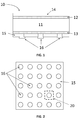
- FIG. 1 A cross section of an example of a test structure 10 that may be used in a method according to the present disclosure is shown in Figure 1 . It comprises a silicon substrate 11 of a first dopant type with a first doped region 12 at a first side and a second doped region 13 at a second side of the substrate.
- the first doped region 12 and the second doped region 13 may have a doping type opposite to the doping type of the substrate 11, thus forming p-n junctions underlying the substrate surfaces.
- the first doped region 12 and the second doped region 13 have the same doping profile.
- the first doped region and the second doped region may have the same doping type as the substrate and a higher doping concentration, thus forming high-low junctions.
- the second passivation layer 15 covers the entire surface of the substrate 11 at the second side, apart from locations where dedicated local openings are provided through the second passivation layer 15.
- the test structure 10 further comprises a patterned metal layer, the patterned metal layer comprising a plurality of metal features 16, each of the metal features 16 being provided at the location of a local opening through the second passivation layer 15, and in contact with the underlying silicon.
- the metal features 16 may overlap the edges of the passivation layer 15 at the local openings.
- the test structure 10 thus comprises metal contact areas (areas with metallized surface), where the metal features 16 are in electrical contact with the silicon, and passivated or non-metallized areas/surfaces, where the passivation layer 14, 15 is in contact with the silicon surface (no electrical contact with a metal feature).
- the metal features may be in direct physical contact with the silicon or there may be a thin passivation layer (tunneling layer) in between, resulting in passivated contacts as described above.
- the metal features 16 may for example have a circular shape or a square shape, or any other suitable shape.
- Figure 2 shows a bottom view of the test structure of Figure 1 , with circular metal features.
- Figure 2 only shows 25 circular metal features to illustrate the concept, but in practice the number of metal features may be much higher, such as for example in the range between 10 5 and 10 6 metal features, e.g. spread over an area of 4 cm by 4 cm, the present disclosure not being limited thereto.
- the different metal features 16 are physically separated from one another.
- a characteristic size of the metal features 16 is smaller than the effective minority carrier diffusion length in the metal covered area of the silicon substrate.
- the characteristic size may be the diameter in case of circular metal features or the side length in case of square metal features. This condition results in an approximately constant minority carrier concentration throughout the test structure and therefore enables a simpler interpretation of the measurements (as further described).
- the spacing (distance) between neighboring metal features 16 is much smaller than the effective diffusion length in the passivated (non-metallized) area of the silicon substrate.
- both the lateral size of the metal features and the distance between neighboring metal features are typically in the sub-millimeter range.
- Test structures of the present disclosure comprise at least two, preferably more than two, zones with different metal coverage, i.e. with a different ratio between the contacted area (metallized surface area) and the total zone area.
- a test structure of the present disclosure may for example comprise a plurality of square zones, each of the zones having a different metal coverage. Providing zones with different metal coverage enables separating information on recombination in the non-metallized areas from information related to recombination in metal covered areas.
- the test structure comprises more than two different zones, such as for example nine different zones, each zone having a different metal coverage.
- Each zone may have a size in the order of several square centimeters, such as for example 4 cm x 4 cm.
- each zone of the test structure is composed of a two-dimensional array of identical unit cells 20, as indicated in Figure 2 , the present disclosure not being limited thereto.
- Typical coil frequencies used during radio-wave detected contactless photo-conductance decay measurements are in the 11 MHz range, which corresponds to probing the wafer under test with electromagnetic radiation with a wavelength of about 27 m. Since the wavelength of the radiation by which the test structure is probed is many orders of magnitudes larger than the characteristic size of the metal pattern on the wafer, the equivalent resistance that is observed by the radiation may be found from ordinary electric circuit theory. No wave effects need to be taken into account.
- an approximate expression for the influence of the presence of metal features 16 on the test structure conductivity may be derived.
- An estimation of the influence of metal conductivity on the resistance of the wafer can be obtained by using the equivalent circuit shown in Figure 3 for a unit cell 20 of a test structure of the present disclosure with square metal features 16.
- Each unit cell 20 (as e.g. indicated in Figure 2 ) of a zone of the test structure can be considered as being composed of a first area which is not contacted by metal (but covered by the passivation layer 15) and a second area which is locally shorted by a metal feature 16. Perfect local shunting is assumed here.
- the electrical resistance of the metal layer is assumed to be much smaller than the electrical resistance of the silicon substrate 11.
- the impedance due to the capacitance between metal features 16 is assumed to be much larger than the impedance due to the conductivity of the substrate 11 between metal features.
- Measured photo-conductance data need to be corrected to obtain the wafer conductance.
- the correction factor depends on the test structure geometry.
- wafer conductivity ⁇ Si is related to the measured conductivity ⁇ meas by equation (5).
- ⁇ meas ⁇ Si 1 + 4 C met ⁇ ⁇ 2 ⁇ C met
- wafer conductivity ⁇ Si is related to the measured conductivity ⁇ meas by equation (6).
- ⁇ meas ⁇ Si 1 + C met 3 / 2 1 ⁇ C met
- Finite contact resistance causes local shorting of the device under test to be imperfect. More specifically, it approximately takes a transfer length L T for current to flow from the semiconductor to the metal, wherein the transfer length equals contact resistance divided by sheet resistance.
- the transfer length effect can approximately be taken into account by considering that the effective metal dot size is approximately reduced by twice the transfer length: one transfer length for the current to flow from semiconductor to metal and one transfer length for current to flow back again.
- C met can be substituted by C eff to estimate the effect of finite contact resistance on correction factors due to metal coverage. Similar expressions may be derived for test structures comprising an array of metal dots with a different shape, such as for example an array of square metal dots. These corrections are only applicable if L t is smaller than d. If L t is much larger than the characteristic size d , the effect of local shunting due to the presence of metal may be negligible.
- the recombination characteristics are extracted from effective lifetime measurements as a function of metallized area coverage using test structures as described above, and using photo-conductance decay measurements.
- test structure used in a method of the present disclosure has two such areas with different recombination characteristics.
- a test structure as shown in Figure 1 is assumed.
- the first area is a two-side passivated region, e.g. having a Si-SiO 2 interface at both surfaces.
- the recombination rate in the first area is given by equation (11), wherein R diel is the recombination rate at a passivated (non-metallized) surface and R bulk is the recombination rate in the silicon bulk of the test structure. It is further assumed that passivated areas have the same surface passivation at both sides.
- R 1 2 R diel + R bulk
- the second area of the test structure has the same surface passivation as the first area on a first side of the substrate and has different recombination characteristics at the second side of the substrate.
- the surface in the second area may for example comprise a silicon-air interface, a silicon-metal interface, or silicon - passivated contact interface.
- a passivated contact can for example comprise a dielectric-metal stack, a dielectric-polysilicon-metal stack, or an amorphous silicon-metal stack, the present disclosure not being limited thereto.
- the recombination rate in the second area of a test structure of the present disclosure is given by equation (12), wherein R met is the recombination rate at the silicon-metal interface.
- R 2 R diel + R met + R bulk
- the difference between the recombination rate at the metallized and passivated (non-metallized) surfaces ( R met - R diel ) can be extracted from the slope of the recombination rate R versus metal surface coverage fraction C met .
- the substrate is an n-type silicon wafer having at both sides a p-type diffused region (emitter region). It is assumed that the injection level is constant over the substrate thickness (in the bulk of the substrate), and over the entire substrate area. This is a reasonable assumption for wafers with an emitter region (or a back surface field region) at the front side and at the back side if the wafer thickness and the contact opening size (size of the metal features) are both much smaller than the minority carrier diffusion length.
- ⁇ p is the injection level at the bulk-side of the space charge region between emitter and bulk and N D is the doping concentration in the bulk of the wafer.
- R bulk ⁇ pW / ⁇ bulk
- W the distance between the emitter space charge regions at the first side and at the second side of the test structure, which is approximately equal to the substrate thickness. It is assumed that the bulk injection level ⁇ p is constant over the wafer thickness. This is the case if the bulk minority carrier diffusion length is much larger than the wafer thickness.
- ⁇ eff is the global effective lifetime of the test structure
- ⁇ bulk is the minority carrier lifetime in the bulk of the wafer
- N D is the doping concentration in the bulk of the wafer
- ⁇ p is the injection level in the bulk of the wafer. The injection level is assumed to be constant over the wafer thickness in the bulk of the wafer and in the plane of the test structure.
- q is the electron charge
- n i is the intrinsic carrier density
- W is the wafer thickness (more accurately: the distance between the space charge regions of both emitter regions).
- J 0,met - J 0,diel can be extracted from the slope of the inverse effective lifetime ( 1 / ⁇ eff ) measured by photo-conductance decay versus metal coverage (C met ). Both ⁇ eff and ⁇ p are the quantities extracted from the photo-conductance measurements. Both may need to be corrected for local shunting due to the presence of metal features before they are used to calculate recombination parameters. As further described, for steady state and generalized photo-conductance measurements, both injection level and lifetime need to be corrected. For transient measurements, only the injection level needs to be corrected.
- J 0,tot can be extracted from the slope of 1 / ⁇ eff as a function of injection level.
- Equations (3) and (4) show that even though the resistance of the test structures of the present disclosure remains dominated by the silicon substrate, metal coverage does have an influence on the resistance of the wafer. This results in an influence on the measured injection levels during photo-conductance measurements and on the measured effective lifetimes. The influence on measured effective lifetime depends on the mode in which the conductivity measurement is done, as described below.
- the injection level is over-estimated in photo conductance measurements on partly metal covered wafers due to local shunting by the metal layers.
- ⁇ eff is an effective lifetime and G is the generation rate, being defined as the number of minority carriers generated in the wafer per second and per unit volume. Therefore, misinterpretations of the injection level may result in errors on the measured effective lifetimes and a correction needs to be made.
- the method of the present disclosure is described above mainly for the determination of saturation currents on test structures with p-n junctions, the method may also be used for determining recombination characteristics on test structures without p-n junctions. For example, for samples with high-low junctions (n + -n junctions or p + -p junctions) or for samples without any junction, recombination characteristics at metallized surfaces may also be measured using a test structure of the present disclosure.
- ⁇ eff is the effective lifetime
- ⁇ b is a bulk minority carrier lifetime
- S p is the effective surface recombination velocity at the passivated (non-metallized) surface
- S m is the effective surface recombination velocity at the metal covered surface
- C m is the metal coverage
- W wafer thickness
- test structure of the present disclosure may also be used to determine effective lifetimes instead of saturation current densities or surface recombination velocities.
- 1 ⁇ eff 1 ⁇ b + C met 1 ⁇ m ⁇ 1 ⁇ p
- ⁇ eff is an effective lifetime for the entire test structure (i.e. the measured quantity as a function of metal coverage)
- ⁇ p is the effective lifetime in passivated (non-metallized) areas
- ⁇ m is the effective lifetime in metal covered areas.
- Methods of the present disclosure may advantageously be used for saturation current density extraction of metallized emitters of e.g. photovoltaic cells.
- saturation current extraction was done for test structures with Al contacts on diffused boron emitters.
- recombination characteristics were determined for test structures with Al contacts on test structures comprising high/low junctions (e.g. as in a back surface field region of photovoltaic cells) and for test structures without any diffused regions. All measurements were done using a steady state analysis.
- n-type Cz Si wafers with a bulk resistivity of 3 to 8 Ohm-cm were used in the experiments.
- An experimental split was made between: (a) wafers with an emitter diffusion (p + diffusion forming a p-n junction at both wafer sides); (b) wafers with a back surface field diffusion (n + diffusion forming a high-low junction at both wafer sides); and (c) wafers without any diffusion.
- a thermally grown silicon oxide layer was used as a passivation layer.
- each passivated wafer was divided into nine zones, in which different fractions C met were provided.
- Circular openings with 15 micrometer diameter were lithographically defined and etched through the passivation layer.
- the nominal coverage of the exposed region ranged from 0% to 17% (0%, 1.25%, 2.5%, 5%, 7.5%, 10%, 12.5%, 15%, 17%). Due to possible over-etching or under-etching and/or over-development or under-development during lithographical definition of the contact openings, the actual coverage may be somewhat different.
- the distance between the openings varied between 118.9 micrometer for the zone with 1.25% coverage and 32.2 micrometer for the zone with 17% coverage. In all zones, circular metal dots with a diameter of 15 micrometer were used.
- a 0.5 micrometer thick Al layer was subsequently sputtered on the wafer and etched such that only the exposed silicon regions remained covered. Then a forming gas anneal was done.
- Effective lifetime measurements were done on these test structures in accordance with a method of the present disclosure. For each of the 9 zones with different metal coverage of the test structure a quasi-steady state photo-conductance (QSSPC) measurement was done. Each QSSPC measurement yields effective lifetimes as a function of injection level. Thus, results are obtained as a function of metal coverage and as a function of injection level.
- QSSPC quasi-steady state photo-conductance
- Figure 4 shows the difference between the saturation current density J 0,met of the metallized emitter and the saturation current density J 0,diel of the non-metallized emitter as a function of injection level, as determined using a method according to the present disclosure. Error bars are 95% confidence intervals. For emitters with good surface passivation and with non-passivated metal contact as in the test structure used in the experiment, it may be assumed that J 0,met is much larger than J 0,diel , therefore J 0,met - J 0,diel ⁇ J 0,met . Therefore the data shown in Figure 4 can be considered as a lower limit for the saturation current density of the metallized emitter.
- Figure 5 shows the difference between the saturation current density of the metallized back surface field region and the saturation current density of the non-metallized back surface field region as a function of injection level, as in Figure 4 , but for a test structure with a high-low junction instead of a p-n junction at both sides of the wafer.
- Figure 6 shows the extracted saturation currents for test structures with an emitter diffusion at both sides of the test structure.
- Figure 6 shows the effective J 0 , diel incorporating the effect of bulk recombination and recombination in the passivated (non-metallized) emitter.
- the intercept has a contribution from bulk recombination and a contribution from recombination in the passivated emitter. It was assumed that the bulk recombination component is negligible compared to the recombination component in the passivated emitter. Therefore, the estimate for J 0 , diel shown in Figure 6 is an upper limit for J 0 , diel since there is a (small) contribution from bulk recombination which was not taken into account.
- Figure 7 shows the extracted saturation current density for test structures with a back surface field region (high-low junction) at both sides.
- Figure 8 shows the difference between the surface recombination velocity at the metal-semiconductor interface S met and the surface recombination velocity at the non-metallized semiconductor surface S diel as a function of injection level for test structures without diffused regions. Error bars are 95% confidence intervals. For samples with good surface passivation and with non-passivated metal contacts as in the test structure used in the experiment, it may be assumed that S met is much larger than S diel , therefore S met - S diel ⁇ S met . The values shown in Figure 8 can therefore be considered as a lower limit for S met .
- Figure 9 shows the extracted surface recombination velocity for test structures without a diffused region.
- Figure 10 shows the inverse effective lifetime as a function of metal coverage for a sample with an emitter diffusion at both sides.
- Figure 10 shows both the as-measured effective lifetime and the effective lifetime that was corrected for the effect of local shorting due to the presence of the metal, at an injection level of 7.10 15 cm -3 . It can be seen that the correction for local shunting due to the presence of metal increases the slope of inverse effective lifetime versus metal coverage.
- effective lifetime measurements may be interpreted in several ways:
Landscapes
- Health & Medical Sciences (AREA)
- Physics & Mathematics (AREA)
- Life Sciences & Earth Sciences (AREA)
- Chemical & Material Sciences (AREA)
- General Physics & Mathematics (AREA)
- Pathology (AREA)
- Immunology (AREA)
- Analytical Chemistry (AREA)
- Biochemistry (AREA)
- General Health & Medical Sciences (AREA)
- Nuclear Medicine, Radiotherapy & Molecular Imaging (AREA)
- Engineering & Computer Science (AREA)
- Medicinal Chemistry (AREA)
- Food Science & Technology (AREA)
- Electromagnetism (AREA)
- Toxicology (AREA)
- Testing Or Measuring Of Semiconductors Or The Like (AREA)
- Automation & Control Theory (AREA)
- Manufacturing & Machinery (AREA)
Claims (14)
- Verfahren zum Bestimmen einer Rekombinationscharakteristik an einer Halbleiteroberfläche, wobei das Verfahren umfasst:Bereitstellen einer Teststruktur (10), wobei die Teststruktur umfasst:ein Halbleitersubstrat (11) mit einer ersten Oberfläche und einer zweiten Oberfläche gegenüber der ersten Oberfläche;eine erste Passivierungsschicht (14) auf der ersten Oberfläche;eine zweite Passivierungsschicht (15) auf der zweiten Oberfläche, wobei die zweite Passivierungsschicht mehrere Öffnungen an vorbestimmten Stellen aufweist; undmehrere Metallmerkmale (16) in Kontakt mit der zweiten Halbleiteroberfläche an den vorbestimmten Stellen, wodurch metallisierte Oberflächen an den vorbestimmten Stellen und nicht metallisierte Oberflächen außerhalb der vorbestimmten Stellen gebildet werden,wobei eine charakteristische Größe der Metallmerkmale (16) kleiner ist als eine effektive Diffusionslänge in dem darunterliegenden Halbleiter an den vorbestimmten Stellen und die Metallmerkmale mit einem kleineren Abstand als eine effektive Diffusionslänge in dem darunterliegenden Halbleiter außerhalb der vorbestimmten Stellen bereitgestellt sind, wobei die Metallmerkmale in mehreren Zonen gruppiert sind, wobei jede der mehreren Zonen einen anderen Metallbedeckungsgrad aufweist, wobei der Metallbedeckungsgrad das Verhältnis zwischen dem metallisierten Oberflächenbereich und dem Gesamtbereich ist;Durchführen einer Fotokonduktanz-Zerfallsmessung (Photo-Conductance Decay-Messung) in jeder der mehreren Zonen, wodurch effektive Lebensdauerwerte für verschiedene Injektionsniveaus als Funktion des Metallabdeckungsgrades bestimmt werden; undExtrahieren der Rekombinationscharakteristik aus den gemessenen effektiven Lebensdauerwerten.
- Verfahren nach Anspruch 1, wobei das Extrahieren der Rekombinationscharakteristik aus den gemessenen effektiven Lebensdauerwerten ein Bestimmen einer Differenz zwischen der Rekombinationscharakteristik an einer metallisierten Oberfläche und der Rekombinationscharakteristik an einer nicht metallisierten Oberfläche für jedes der Injektionsniveaus aus der Steigung einer linearen Anpassung von inverser effektiver Lebensdauer im Verhältnis zum Metallabdeckungsgrad umfasst.
- Verfahren nach Anspruch 1, wobei das Extrahieren der Rekombinationscharakteristik ein Bestimmen eines oberen Wertes der Rekombinationscharakteristik an einer nicht metallisierten Oberfläche für jedes der Injektionsniveaus aus dem Achsabschnitt einer linearen Anpassung von inverser effektiver Lebensdauer gegenüber Metallabdeckungsgrad mit der Null-Metallabdeckungsgradachse umfasst.
- Verfahren nach einem der Ansprüche 1 bis 3, wobei die Rekombinationscharakteristik eine Oberflächenrekombinationsgeschwindigkeit ist.
- Verfahren nach einem der Ansprüche 1 bis 3, wobei die Rekombinationscharakteristik eine Sättigungsstromdichte ist.
- Verfahren nach einem der Ansprüche 1 bis 3, wobei die Rekombinationscharakteristik eine inverse Lebensdauer ist.
- Verfahren nach einem der Ansprüche 1 bis 3, wobei das Halbleitersubstrat eine erste dotierte Region (12), die einen ersten p-n-Übergang bildet, der unter der ersten Oberfläche liegt, und eine zweite dotierte Region (13), die einen zweiten p-n-Übergang bildet, der unter der zweiten Oberfläche liegt, umfasst und wobei die Rekombinationscharakteristik eine Sättigungsstromdichte ist.
- Verfahren nach Anspruch 1, wobei das Halbleitersubstrat einen ersten p-n-Übergang, der unter der ersten Oberfläche liegt, und einen zweiten p-n-Übergang, der unter der zweiten Oberfläche liegt, umfasst und wobei ein Extrahieren der Rekombinationscharakteristik ein Bestimmen einer gesamten Sättigungsstromdichte bei hoher Injektion für jeden Metallabdeckungsgrad aus der Steigung einer inversen Lebensdauer im Verhältnis zum Injektionsniveau, Durchführen einer Korrektur der effektiven Lebensdauerwerte für eine Auger-Rekombination und danach ein Extrahieren der Sättigungsstromdichte an einer metallisierten Oberfläche und der Sättigungsstromdichte an einer nicht metallisierten Oberfläche aus der Steigung einer linearen Anpassung der gesamten Sättigungsstromdichte im Verhältnis zur Metallabdeckung umfasst.
- Verfahren nach einem der Ansprüche 1 bis 3, wobei das Halbleitersubstrat eine erste dotierte Region (12), die einen ersten Hoch/Tief-Übergang bildet, der unter der ersten Oberfläche liegt, und eine zweite dotierte Region (13), die einen zweiten Hoch/Tief-Übergang bildet, der unter der zweiten Oberfläche liegt, umfasst und wobei die Rekombinationscharakteristik eine Sättigungsstromdichte ist.
- Verfahren nach Anspruch 1, wobei das Halbleitersubstrat einen ersten Hoch/Tief-Übergang, der unter der ersten Oberfläche liegt, und einen zweiten Hoch/Tief-Übergang, der unter der zweiten Oberfläche liegt, umfasst und wobei ein Extrahieren der Rekombinationscharakteristik ein Bestimmen der gesamten Sättigungsstromdichte bei hoher Injektion für jeden Metallabdeckungsgrad aus der Steigung von inverser effektiver Lebensdauer im Verhältnis zum Injektionsniveau, Durchführen einer Korrektur der effektiven Lebensdauerwerte für eine Auger-Rekombination und danach ein Extrahieren der Sättigungsstromdichte an einer metallisierten Oberfläche und der Sättigungsstromdichte an einer nicht metallisierten Oberfläche aus der Steigung einer linearen Anpassung der gesamten Sättigungsstromdichte im Verhältnis zur Metallabdeckung umfasst.
- Verfahren nach einem der vorangehenden Ansprüche, wobei das Halbleitersubstrat ein Siliziumsubstrat ist.
- Verfahren nach einem der vorangehenden Ansprüche, des Weiteren umfassend eine Korrektur der gemessenen Injektionsniveaus und effektiven Lebensdauerwerte unter Berücksichtigung des Einflusses einer Metallleitfähigkeit, vor dem Extrahieren der Rekombinationscharakteristik.
- Verfahren nach einem der vorangehenden Ansprüche, wobei die erste Passivierungsschicht eine kontinuierliche Schicht ist, welche die erste Oberfläche bedeckt.
- Verwendung des Verfahrens nach einem der vorangehenden Ansprüche zum Bestimmen von Rekombinationscharakteristiken von Emitterkontakten oder Basiskontakten von Photovoltaikzellen.
Priority Applications (3)
| Application Number | Priority Date | Filing Date | Title |
|---|---|---|---|
| EP13185659.3A EP2851696B1 (de) | 2013-09-24 | 2013-09-24 | Verfahren zur Extraktion von Rekombinationsmerkmalen an metallisierten Halbleiteroberflächen |
| JP2014185502A JP6272741B2 (ja) | 2013-09-24 | 2014-09-11 | メタライズ半導体表面での再結合特性の抽出方法 |
| US14/495,607 US9465069B2 (en) | 2013-09-24 | 2014-09-24 | Method for the extraction of recombination characteristics at metallized semiconductor surfaces |
Applications Claiming Priority (1)
| Application Number | Priority Date | Filing Date | Title |
|---|---|---|---|
| EP13185659.3A EP2851696B1 (de) | 2013-09-24 | 2013-09-24 | Verfahren zur Extraktion von Rekombinationsmerkmalen an metallisierten Halbleiteroberflächen |
Publications (2)
| Publication Number | Publication Date |
|---|---|
| EP2851696A1 EP2851696A1 (de) | 2015-03-25 |
| EP2851696B1 true EP2851696B1 (de) | 2016-04-20 |
Family
ID=49261452
Family Applications (1)
| Application Number | Title | Priority Date | Filing Date |
|---|---|---|---|
| EP13185659.3A Not-in-force EP2851696B1 (de) | 2013-09-24 | 2013-09-24 | Verfahren zur Extraktion von Rekombinationsmerkmalen an metallisierten Halbleiteroberflächen |
Country Status (3)
| Country | Link |
|---|---|
| US (1) | US9465069B2 (de) |
| EP (1) | EP2851696B1 (de) |
| JP (1) | JP6272741B2 (de) |
Families Citing this family (7)
| Publication number | Priority date | Publication date | Assignee | Title |
|---|---|---|---|---|
| EP2993699B1 (de) * | 2014-09-04 | 2018-03-21 | IMEC vzw | Verfahren zur Herstellung kristalliner photovoltaischer Zellen |
| USD868604S1 (en) * | 2016-03-18 | 2019-12-03 | General Electric Company | Sensor |
| CN110349875B (zh) * | 2018-04-03 | 2021-07-09 | 江苏微导纳米科技股份有限公司 | 一种测量晶圆表面电荷密度变化的方法 |
| CN115728273B (zh) * | 2021-08-31 | 2024-11-15 | 环晟光伏(江苏)有限公司 | 一种采用pl表征太阳电池金属复合的方法 |
| US12105136B2 (en) * | 2021-09-09 | 2024-10-01 | Kla Corporation | Method for determining material parameters of a multilayer test sample |
| KR102699160B1 (ko) * | 2021-12-16 | 2024-08-27 | 한국에너지기술연구원 | 실리콘 태양전지의 재결합 손실 계측방법 및 이를 이용한 실리콘 태양전지의 설계 방법 |
| CN115166460B (zh) * | 2022-06-29 | 2025-09-05 | 泰州中来光电科技有限公司 | 一种测试晶体硅体区复合的方法 |
Family Cites Families (10)
| Publication number | Priority date | Publication date | Assignee | Title |
|---|---|---|---|---|
| JPH0291957A (ja) * | 1988-09-28 | 1990-03-30 | Fujitsu Ltd | ライフタイム測定装置 |
| US5081414A (en) * | 1989-03-20 | 1992-01-14 | Semitex Co., Ltd. | Method for measuring lifetime of semiconductor material and apparatus therefor |
| JP3810207B2 (ja) * | 1998-04-28 | 2006-08-16 | 株式会社アドバンテスト | 半導体パラメータの測定方法および測定装置 |
| DE102005040010A1 (de) * | 2005-08-23 | 2007-03-15 | Rwe Schott Solar Gmbh | Verfahren und Vorrichtung zur Ermittlung von Produktionsfehlern in einem Halbleiterbau-element |
| JP5273635B2 (ja) * | 2006-08-25 | 2013-08-28 | 独立行政法人産業技術総合研究所 | 高効率間接遷移型半導体紫外線発光素子 |
| DE102006049683B3 (de) * | 2006-10-13 | 2008-05-29 | Q-Cells Ag | Verfahren und Vorrichtung zum Charakterisieren von Wafern bei der Herstellung von Solarzellen |
| ATE514095T1 (de) * | 2007-09-11 | 2011-07-15 | Soitec Silicon On Insulator | Volumenlebensdauermessung |
| JP5504634B2 (ja) * | 2009-01-27 | 2014-05-28 | 信越半導体株式会社 | ライフタイムの評価方法 |
| US20110308603A1 (en) * | 2010-06-17 | 2011-12-22 | Katholieke Universiteit Leuven | Method for passivating a silicon surface |
| US8604447B2 (en) * | 2011-07-27 | 2013-12-10 | Kla-Tencor Corporation | Solar metrology methods and apparatus |
-
2013
- 2013-09-24 EP EP13185659.3A patent/EP2851696B1/de not_active Not-in-force
-
2014
- 2014-09-11 JP JP2014185502A patent/JP6272741B2/ja not_active Expired - Fee Related
- 2014-09-24 US US14/495,607 patent/US9465069B2/en not_active Expired - Fee Related
Also Published As
| Publication number | Publication date |
|---|---|
| JP6272741B2 (ja) | 2018-01-31 |
| US20150084661A1 (en) | 2015-03-26 |
| US9465069B2 (en) | 2016-10-11 |
| EP2851696A1 (de) | 2015-03-25 |
| JP2015065435A (ja) | 2015-04-09 |
Similar Documents
| Publication | Publication Date | Title |
|---|---|---|
| US9465069B2 (en) | Method for the extraction of recombination characteristics at metallized semiconductor surfaces | |
| Sinton et al. | A quasi-steady-state open-circuit voltage method for solar cell characterization | |
| Sinton et al. | Contactless determination of current–voltage characteristics and minority‐carrier lifetimes in semiconductors from quasi‐steady‐state photoconductance data | |
| Metzger et al. | Analysis of charge separation dynamics in a semiconductor junction | |
| Bolotnikov et al. | Factors limiting the performance of CdZnTe detectors | |
| Van der Heide et al. | Explanation of high solar cell diode factors by nonuniform contact resistance | |
| US6265890B1 (en) | In-line non-contact depletion capacitance measurement method and apparatus | |
| CN108196110B (zh) | 一种金属半导体界面复合电流密度的测试方法及装置 | |
| Recart et al. | Application of junction capacitance measurements to the characterization of solar cells | |
| US10027278B2 (en) | Characterization of substrate doping and series resistance during solar cell efficiency measurement | |
| Dumbrell et al. | Comparison of terminal and implied open-circuit voltage measurements | |
| Palm | Local investigation of recombination at grain boundaries in silicon by grain boundary‐electron beam induced current | |
| Kökbudak et al. | On the determination of the contact resistivity for passivating contacts using 3D simulations | |
| Metzger | How lifetime fluctuations, grain-boundary recombination, and junctions affect lifetime measurements and their correlation to silicon solar cell performance | |
| US20030059966A1 (en) | Non- contacting capacitive diagnostic device | |
| Deckers et al. | Injection dependent emitter saturation current density measurement under metallized areas using photoconductance decay | |
| Inns et al. | Measurement of metal induced recombination in solar cells | |
| US9310396B2 (en) | Apparatus and methods of measuring minority carrier lifetime using a liquid probe | |
| Römer et al. | Counterdoping with patterned ion implantation | |
| Ong et al. | Determination of diffusion length from within a confined region with the use of EBIC | |
| Thomson et al. | Uncertainty in photoconductance measurements of the emitter saturation current | |
| Cuevas et al. | Characterization and diagnosis of silicon wafers, ingots, and solar cells | |
| Fellmeth | Silicon solar cells for the application in low concentrator systems-development and characterization | |
| Turkay et al. | Spreading resistance modeling for contact resistivity extraction in ohmic multilayer structures with circular electrodes | |
| Eranen et al. | Silicon semi 3D radiation detectors |
Legal Events
| Date | Code | Title | Description |
|---|---|---|---|
| PUAI | Public reference made under article 153(3) epc to a published international application that has entered the european phase |
Free format text: ORIGINAL CODE: 0009012 |
|
| 17P | Request for examination filed |
Effective date: 20130924 |
|
| AK | Designated contracting states |
Kind code of ref document: A1 Designated state(s): AL AT BE BG CH CY CZ DE DK EE ES FI FR GB GR HR HU IE IS IT LI LT LU LV MC MK MT NL NO PL PT RO RS SE SI SK SM TR |
|
| AX | Request for extension of the european patent |
Extension state: BA ME |
|
| R17P | Request for examination filed (corrected) |
Effective date: 20150827 |
|
| RBV | Designated contracting states (corrected) |
Designated state(s): AL AT BE BG CH CY CZ DE DK EE ES FI FR GB GR HR HU IE IS IT LI LT LU LV MC MK MT NL NO PL PT RO RS SE SI SK SM TR |
|
| GRAP | Despatch of communication of intention to grant a patent |
Free format text: ORIGINAL CODE: EPIDOSNIGR1 |
|
| RIC1 | Information provided on ipc code assigned before grant |
Ipc: G01N 21/64 20060101ALI20160112BHEP Ipc: G01R 31/26 20060101AFI20160112BHEP Ipc: H01L 21/66 20060101ALI20160112BHEP Ipc: H02S 50/00 20140101ALI20160112BHEP |
|
| GRAS | Grant fee paid |
Free format text: ORIGINAL CODE: EPIDOSNIGR3 |
|
| INTG | Intention to grant announced |
Effective date: 20160203 |
|
| GRAA | (expected) grant |
Free format text: ORIGINAL CODE: 0009210 |
|
| AK | Designated contracting states |
Kind code of ref document: B1 Designated state(s): AL AT BE BG CH CY CZ DE DK EE ES FI FR GB GR HR HU IE IS IT LI LT LU LV MC MK MT NL NO PL PT RO RS SE SI SK SM TR |
|
| REG | Reference to a national code |
Ref country code: GB Ref legal event code: FG4D |
|
| REG | Reference to a national code |
Ref country code: CH Ref legal event code: EP |
|
| REG | Reference to a national code |
Ref country code: AT Ref legal event code: REF Ref document number: 793026 Country of ref document: AT Kind code of ref document: T Effective date: 20160515 |
|
| REG | Reference to a national code |
Ref country code: IE Ref legal event code: FG4D |
|
| REG | Reference to a national code |
Ref country code: DE Ref legal event code: R096 Ref document number: 602013006670 Country of ref document: DE |
|
| REG | Reference to a national code |
Ref country code: FR Ref legal event code: PLFP Year of fee payment: 4 |
|
| REG | Reference to a national code |
Ref country code: DE Ref legal event code: R082 Ref document number: 602013006670 Country of ref document: DE |
|
| REG | Reference to a national code |
Ref country code: LT Ref legal event code: MG4D |
|
| REG | Reference to a national code |
Ref country code: AT Ref legal event code: MK05 Ref document number: 793026 Country of ref document: AT Kind code of ref document: T Effective date: 20160420 |
|
| REG | Reference to a national code |
Ref country code: NL Ref legal event code: MP Effective date: 20160420 |
|
| PG25 | Lapsed in a contracting state [announced via postgrant information from national office to epo] |
Ref country code: NO Free format text: LAPSE BECAUSE OF FAILURE TO SUBMIT A TRANSLATION OF THE DESCRIPTION OR TO PAY THE FEE WITHIN THE PRESCRIBED TIME-LIMIT Effective date: 20160720 Ref country code: FI Free format text: LAPSE BECAUSE OF FAILURE TO SUBMIT A TRANSLATION OF THE DESCRIPTION OR TO PAY THE FEE WITHIN THE PRESCRIBED TIME-LIMIT Effective date: 20160420 Ref country code: PL Free format text: LAPSE BECAUSE OF FAILURE TO SUBMIT A TRANSLATION OF THE DESCRIPTION OR TO PAY THE FEE WITHIN THE PRESCRIBED TIME-LIMIT Effective date: 20160420 Ref country code: LT Free format text: LAPSE BECAUSE OF FAILURE TO SUBMIT A TRANSLATION OF THE DESCRIPTION OR TO PAY THE FEE WITHIN THE PRESCRIBED TIME-LIMIT Effective date: 20160420 Ref country code: NL Free format text: LAPSE BECAUSE OF FAILURE TO SUBMIT A TRANSLATION OF THE DESCRIPTION OR TO PAY THE FEE WITHIN THE PRESCRIBED TIME-LIMIT Effective date: 20160420 |
|
| PG25 | Lapsed in a contracting state [announced via postgrant information from national office to epo] |
Ref country code: AT Free format text: LAPSE BECAUSE OF FAILURE TO SUBMIT A TRANSLATION OF THE DESCRIPTION OR TO PAY THE FEE WITHIN THE PRESCRIBED TIME-LIMIT Effective date: 20160420 Ref country code: RS Free format text: LAPSE BECAUSE OF FAILURE TO SUBMIT A TRANSLATION OF THE DESCRIPTION OR TO PAY THE FEE WITHIN THE PRESCRIBED TIME-LIMIT Effective date: 20160420 Ref country code: ES Free format text: LAPSE BECAUSE OF FAILURE TO SUBMIT A TRANSLATION OF THE DESCRIPTION OR TO PAY THE FEE WITHIN THE PRESCRIBED TIME-LIMIT Effective date: 20160420 Ref country code: PT Free format text: LAPSE BECAUSE OF FAILURE TO SUBMIT A TRANSLATION OF THE DESCRIPTION OR TO PAY THE FEE WITHIN THE PRESCRIBED TIME-LIMIT Effective date: 20160822 Ref country code: LV Free format text: LAPSE BECAUSE OF FAILURE TO SUBMIT A TRANSLATION OF THE DESCRIPTION OR TO PAY THE FEE WITHIN THE PRESCRIBED TIME-LIMIT Effective date: 20160420 Ref country code: HR Free format text: LAPSE BECAUSE OF FAILURE TO SUBMIT A TRANSLATION OF THE DESCRIPTION OR TO PAY THE FEE WITHIN THE PRESCRIBED TIME-LIMIT Effective date: 20160420 Ref country code: SE Free format text: LAPSE BECAUSE OF FAILURE TO SUBMIT A TRANSLATION OF THE DESCRIPTION OR TO PAY THE FEE WITHIN THE PRESCRIBED TIME-LIMIT Effective date: 20160420 Ref country code: GR Free format text: LAPSE BECAUSE OF FAILURE TO SUBMIT A TRANSLATION OF THE DESCRIPTION OR TO PAY THE FEE WITHIN THE PRESCRIBED TIME-LIMIT Effective date: 20160721 |
|
| PG25 | Lapsed in a contracting state [announced via postgrant information from national office to epo] |
Ref country code: IT Free format text: LAPSE BECAUSE OF FAILURE TO SUBMIT A TRANSLATION OF THE DESCRIPTION OR TO PAY THE FEE WITHIN THE PRESCRIBED TIME-LIMIT Effective date: 20160420 Ref country code: BE Free format text: LAPSE BECAUSE OF FAILURE TO SUBMIT A TRANSLATION OF THE DESCRIPTION OR TO PAY THE FEE WITHIN THE PRESCRIBED TIME-LIMIT Effective date: 20160420 |
|
| REG | Reference to a national code |
Ref country code: DE Ref legal event code: R097 Ref document number: 602013006670 Country of ref document: DE |
|
| PG25 | Lapsed in a contracting state [announced via postgrant information from national office to epo] |
Ref country code: DK Free format text: LAPSE BECAUSE OF FAILURE TO SUBMIT A TRANSLATION OF THE DESCRIPTION OR TO PAY THE FEE WITHIN THE PRESCRIBED TIME-LIMIT Effective date: 20160420 Ref country code: CZ Free format text: LAPSE BECAUSE OF FAILURE TO SUBMIT A TRANSLATION OF THE DESCRIPTION OR TO PAY THE FEE WITHIN THE PRESCRIBED TIME-LIMIT Effective date: 20160420 Ref country code: EE Free format text: LAPSE BECAUSE OF FAILURE TO SUBMIT A TRANSLATION OF THE DESCRIPTION OR TO PAY THE FEE WITHIN THE PRESCRIBED TIME-LIMIT Effective date: 20160420 Ref country code: SK Free format text: LAPSE BECAUSE OF FAILURE TO SUBMIT A TRANSLATION OF THE DESCRIPTION OR TO PAY THE FEE WITHIN THE PRESCRIBED TIME-LIMIT Effective date: 20160420 Ref country code: RO Free format text: LAPSE BECAUSE OF FAILURE TO SUBMIT A TRANSLATION OF THE DESCRIPTION OR TO PAY THE FEE WITHIN THE PRESCRIBED TIME-LIMIT Effective date: 20160420 |
|
| PLBE | No opposition filed within time limit |
Free format text: ORIGINAL CODE: 0009261 |
|
| STAA | Information on the status of an ep patent application or granted ep patent |
Free format text: STATUS: NO OPPOSITION FILED WITHIN TIME LIMIT |
|
| PG25 | Lapsed in a contracting state [announced via postgrant information from national office to epo] |
Ref country code: SM Free format text: LAPSE BECAUSE OF FAILURE TO SUBMIT A TRANSLATION OF THE DESCRIPTION OR TO PAY THE FEE WITHIN THE PRESCRIBED TIME-LIMIT Effective date: 20160420 |
|
| 26N | No opposition filed |
Effective date: 20170123 |
|
| PG25 | Lapsed in a contracting state [announced via postgrant information from national office to epo] |
Ref country code: MC Free format text: LAPSE BECAUSE OF FAILURE TO SUBMIT A TRANSLATION OF THE DESCRIPTION OR TO PAY THE FEE WITHIN THE PRESCRIBED TIME-LIMIT Effective date: 20160420 |
|
| REG | Reference to a national code |
Ref country code: CH Ref legal event code: PL |
|
| PG25 | Lapsed in a contracting state [announced via postgrant information from national office to epo] |
Ref country code: SI Free format text: LAPSE BECAUSE OF FAILURE TO SUBMIT A TRANSLATION OF THE DESCRIPTION OR TO PAY THE FEE WITHIN THE PRESCRIBED TIME-LIMIT Effective date: 20160420 |
|
| REG | Reference to a national code |
Ref country code: IE Ref legal event code: MM4A |
|
| PG25 | Lapsed in a contracting state [announced via postgrant information from national office to epo] |
Ref country code: CH Free format text: LAPSE BECAUSE OF NON-PAYMENT OF DUE FEES Effective date: 20160930 Ref country code: LI Free format text: LAPSE BECAUSE OF NON-PAYMENT OF DUE FEES Effective date: 20160930 Ref country code: IE Free format text: LAPSE BECAUSE OF NON-PAYMENT OF DUE FEES Effective date: 20160924 |
|
| REG | Reference to a national code |
Ref country code: FR Ref legal event code: PLFP Year of fee payment: 5 |
|
| PG25 | Lapsed in a contracting state [announced via postgrant information from national office to epo] |
Ref country code: LU Free format text: LAPSE BECAUSE OF NON-PAYMENT OF DUE FEES Effective date: 20160924 |
|
| PG25 | Lapsed in a contracting state [announced via postgrant information from national office to epo] |
Ref country code: HU Free format text: LAPSE BECAUSE OF FAILURE TO SUBMIT A TRANSLATION OF THE DESCRIPTION OR TO PAY THE FEE WITHIN THE PRESCRIBED TIME-LIMIT; INVALID AB INITIO Effective date: 20130924 |
|
| PG25 | Lapsed in a contracting state [announced via postgrant information from national office to epo] |
Ref country code: IS Free format text: LAPSE BECAUSE OF FAILURE TO SUBMIT A TRANSLATION OF THE DESCRIPTION OR TO PAY THE FEE WITHIN THE PRESCRIBED TIME-LIMIT Effective date: 20160420 Ref country code: CY Free format text: LAPSE BECAUSE OF FAILURE TO SUBMIT A TRANSLATION OF THE DESCRIPTION OR TO PAY THE FEE WITHIN THE PRESCRIBED TIME-LIMIT Effective date: 20160420 Ref country code: MT Free format text: LAPSE BECAUSE OF NON-PAYMENT OF DUE FEES Effective date: 20160930 Ref country code: MK Free format text: LAPSE BECAUSE OF FAILURE TO SUBMIT A TRANSLATION OF THE DESCRIPTION OR TO PAY THE FEE WITHIN THE PRESCRIBED TIME-LIMIT Effective date: 20160420 |
|
| PG25 | Lapsed in a contracting state [announced via postgrant information from national office to epo] |
Ref country code: BG Free format text: LAPSE BECAUSE OF FAILURE TO SUBMIT A TRANSLATION OF THE DESCRIPTION OR TO PAY THE FEE WITHIN THE PRESCRIBED TIME-LIMIT Effective date: 20160420 |
|
| REG | Reference to a national code |
Ref country code: FR Ref legal event code: PLFP Year of fee payment: 6 |
|
| PG25 | Lapsed in a contracting state [announced via postgrant information from national office to epo] |
Ref country code: AL Free format text: LAPSE BECAUSE OF FAILURE TO SUBMIT A TRANSLATION OF THE DESCRIPTION OR TO PAY THE FEE WITHIN THE PRESCRIBED TIME-LIMIT Effective date: 20160420 Ref country code: TR Free format text: LAPSE BECAUSE OF FAILURE TO SUBMIT A TRANSLATION OF THE DESCRIPTION OR TO PAY THE FEE WITHIN THE PRESCRIBED TIME-LIMIT Effective date: 20160420 |
|
| PGFP | Annual fee paid to national office [announced via postgrant information from national office to epo] |
Ref country code: FR Payment date: 20210819 Year of fee payment: 9 |
|
| PGFP | Annual fee paid to national office [announced via postgrant information from national office to epo] |
Ref country code: GB Payment date: 20210820 Year of fee payment: 9 Ref country code: DE Payment date: 20210818 Year of fee payment: 9 |
|
| REG | Reference to a national code |
Ref country code: DE Ref legal event code: R119 Ref document number: 602013006670 Country of ref document: DE |
|
| GBPC | Gb: european patent ceased through non-payment of renewal fee |
Effective date: 20220924 |
|
| PG25 | Lapsed in a contracting state [announced via postgrant information from national office to epo] |
Ref country code: FR Free format text: LAPSE BECAUSE OF NON-PAYMENT OF DUE FEES Effective date: 20220930 Ref country code: DE Free format text: LAPSE BECAUSE OF NON-PAYMENT OF DUE FEES Effective date: 20230401 |
|
| PG25 | Lapsed in a contracting state [announced via postgrant information from national office to epo] |
Ref country code: GB Free format text: LAPSE BECAUSE OF NON-PAYMENT OF DUE FEES Effective date: 20220924 |