EP2851957B1 - Halbleiterbauelement aus siliciumcarbid - Google Patents
Halbleiterbauelement aus siliciumcarbid Download PDFInfo
- Publication number
- EP2851957B1 EP2851957B1 EP13790103.9A EP13790103A EP2851957B1 EP 2851957 B1 EP2851957 B1 EP 2851957B1 EP 13790103 A EP13790103 A EP 13790103A EP 2851957 B1 EP2851957 B1 EP 2851957B1
- Authority
- EP
- European Patent Office
- Prior art keywords
- layer
- silicon carbide
- plane
- trench
- semiconductor device
- Prior art date
- Legal status (The legal status is an assumption and is not a legal conclusion. Google has not performed a legal analysis and makes no representation as to the accuracy of the status listed.)
- Active
Links
Images


Classifications
-
- H—ELECTRICITY
- H10—SEMICONDUCTOR DEVICES; ELECTRIC SOLID-STATE DEVICES NOT OTHERWISE PROVIDED FOR
- H10D—INORGANIC ELECTRIC SEMICONDUCTOR DEVICES
- H10D12/00—Bipolar devices controlled by the field effect, e.g. insulated-gate bipolar transistors [IGBT]
- H10D12/01—Manufacture or treatment
- H10D12/031—Manufacture or treatment of IGBTs
-
- H—ELECTRICITY
- H10—SEMICONDUCTOR DEVICES; ELECTRIC SOLID-STATE DEVICES NOT OTHERWISE PROVIDED FOR
- H10D—INORGANIC ELECTRIC SEMICONDUCTOR DEVICES
- H10D12/00—Bipolar devices controlled by the field effect, e.g. insulated-gate bipolar transistors [IGBT]
- H10D12/01—Manufacture or treatment
- H10D12/031—Manufacture or treatment of IGBTs
- H10D12/032—Manufacture or treatment of IGBTs of vertical IGBTs
-
- H—ELECTRICITY
- H10—SEMICONDUCTOR DEVICES; ELECTRIC SOLID-STATE DEVICES NOT OTHERWISE PROVIDED FOR
- H10D—INORGANIC ELECTRIC SEMICONDUCTOR DEVICES
- H10D12/00—Bipolar devices controlled by the field effect, e.g. insulated-gate bipolar transistors [IGBT]
- H10D12/411—Insulated-gate bipolar transistors [IGBT]
- H10D12/441—Vertical IGBTs
- H10D12/461—Vertical IGBTs having non-planar surfaces, e.g. having trenches, recesses or pillars in the surfaces of the emitter, base or collector regions
- H10D12/481—Vertical IGBTs having non-planar surfaces, e.g. having trenches, recesses or pillars in the surfaces of the emitter, base or collector regions having gate structures on slanted surfaces, on vertical surfaces, or in grooves, e.g. trench gate IGBTs
-
- H—ELECTRICITY
- H10—SEMICONDUCTOR DEVICES; ELECTRIC SOLID-STATE DEVICES NOT OTHERWISE PROVIDED FOR
- H10D—INORGANIC ELECTRIC SEMICONDUCTOR DEVICES
- H10D30/00—Field-effect transistors [FET]
- H10D30/01—Manufacture or treatment
- H10D30/021—Manufacture or treatment of FETs having insulated gates [IGFET]
- H10D30/028—Manufacture or treatment of FETs having insulated gates [IGFET] of double-diffused metal oxide semiconductor [DMOS] FETs
- H10D30/0291—Manufacture or treatment of FETs having insulated gates [IGFET] of double-diffused metal oxide semiconductor [DMOS] FETs of vertical DMOS [VDMOS] FETs
- H10D30/0297—Manufacture or treatment of FETs having insulated gates [IGFET] of double-diffused metal oxide semiconductor [DMOS] FETs of vertical DMOS [VDMOS] FETs using recessing of the gate electrodes, e.g. to form trench gate electrodes
-
- H—ELECTRICITY
- H10—SEMICONDUCTOR DEVICES; ELECTRIC SOLID-STATE DEVICES NOT OTHERWISE PROVIDED FOR
- H10D—INORGANIC ELECTRIC SEMICONDUCTOR DEVICES
- H10D30/00—Field-effect transistors [FET]
- H10D30/60—Insulated-gate field-effect transistors [IGFET]
- H10D30/64—Double-diffused metal-oxide semiconductor [DMOS] FETs
- H10D30/66—Vertical DMOS [VDMOS] FETs
- H10D30/668—Vertical DMOS [VDMOS] FETs having trench gate electrodes, e.g. UMOS transistors
-
- H—ELECTRICITY
- H10—SEMICONDUCTOR DEVICES; ELECTRIC SOLID-STATE DEVICES NOT OTHERWISE PROVIDED FOR
- H10D—INORGANIC ELECTRIC SEMICONDUCTOR DEVICES
- H10D62/00—Semiconductor bodies, or regions thereof, of devices having potential barriers
- H10D62/10—Shapes, relative sizes or dispositions of the regions of the semiconductor bodies; Shapes of the semiconductor bodies
- H10D62/102—Constructional design considerations for preventing surface leakage or controlling electric field concentration
- H10D62/103—Constructional design considerations for preventing surface leakage or controlling electric field concentration for increasing or controlling the breakdown voltage of reverse-biased devices
- H10D62/104—Constructional design considerations for preventing surface leakage or controlling electric field concentration for increasing or controlling the breakdown voltage of reverse-biased devices having particular shapes of the bodies at or near reverse-biased junctions, e.g. having bevels or moats
-
- H—ELECTRICITY
- H10—SEMICONDUCTOR DEVICES; ELECTRIC SOLID-STATE DEVICES NOT OTHERWISE PROVIDED FOR
- H10D—INORGANIC ELECTRIC SEMICONDUCTOR DEVICES
- H10D62/00—Semiconductor bodies, or regions thereof, of devices having potential barriers
- H10D62/10—Shapes, relative sizes or dispositions of the regions of the semiconductor bodies; Shapes of the semiconductor bodies
- H10D62/13—Semiconductor regions connected to electrodes carrying current to be rectified, amplified or switched, e.g. source or drain regions
- H10D62/149—Source or drain regions of field-effect devices
- H10D62/151—Source or drain regions of field-effect devices of IGFETs
- H10D62/156—Drain regions of DMOS transistors
- H10D62/157—Impurity concentrations or distributions
-
- H—ELECTRICITY
- H10—SEMICONDUCTOR DEVICES; ELECTRIC SOLID-STATE DEVICES NOT OTHERWISE PROVIDED FOR
- H10D—INORGANIC ELECTRIC SEMICONDUCTOR DEVICES
- H10D62/00—Semiconductor bodies, or regions thereof, of devices having potential barriers
- H10D62/80—Semiconductor bodies, or regions thereof, of devices having potential barriers characterised by the materials
- H10D62/83—Semiconductor bodies, or regions thereof, of devices having potential barriers characterised by the materials being Group IV materials, e.g. B-doped Si or undoped Ge
- H10D62/832—Semiconductor bodies, or regions thereof, of devices having potential barriers characterised by the materials being Group IV materials, e.g. B-doped Si or undoped Ge being Group IV materials comprising two or more elements, e.g. SiGe
- H10D62/8325—Silicon carbide
-
- H—ELECTRICITY
- H10—SEMICONDUCTOR DEVICES; ELECTRIC SOLID-STATE DEVICES NOT OTHERWISE PROVIDED FOR
- H10P—GENERIC PROCESSES OR APPARATUS FOR THE MANUFACTURE OR TREATMENT OF DEVICES COVERED BY CLASS H10
- H10P50/00—Etching of wafers, substrates or parts of devices
- H10P50/20—Dry etching; Plasma etching; Reactive-ion etching
- H10P50/24—Dry etching; Plasma etching; Reactive-ion etching of semiconductor materials
- H10P50/242—Dry etching; Plasma etching; Reactive-ion etching of semiconductor materials of Group IV materials
-
- H—ELECTRICITY
- H10—SEMICONDUCTOR DEVICES; ELECTRIC SOLID-STATE DEVICES NOT OTHERWISE PROVIDED FOR
- H10D—INORGANIC ELECTRIC SEMICONDUCTOR DEVICES
- H10D62/00—Semiconductor bodies, or regions thereof, of devices having potential barriers
- H10D62/10—Shapes, relative sizes or dispositions of the regions of the semiconductor bodies; Shapes of the semiconductor bodies
- H10D62/17—Semiconductor regions connected to electrodes not carrying current to be rectified, amplified or switched, e.g. channel regions
- H10D62/393—Body regions of DMOS transistors or IGBTs
-
- H—ELECTRICITY
- H10—SEMICONDUCTOR DEVICES; ELECTRIC SOLID-STATE DEVICES NOT OTHERWISE PROVIDED FOR
- H10D—INORGANIC ELECTRIC SEMICONDUCTOR DEVICES
- H10D62/00—Semiconductor bodies, or regions thereof, of devices having potential barriers
- H10D62/40—Crystalline structures
- H10D62/405—Orientations of crystalline planes
-
- H—ELECTRICITY
- H10—SEMICONDUCTOR DEVICES; ELECTRIC SOLID-STATE DEVICES NOT OTHERWISE PROVIDED FOR
- H10D—INORGANIC ELECTRIC SEMICONDUCTOR DEVICES
- H10D64/00—Electrodes of devices having potential barriers
- H10D64/20—Electrodes characterised by their shapes, relative sizes or dispositions
- H10D64/27—Electrodes not carrying the current to be rectified, amplified, oscillated or switched, e.g. gates
- H10D64/311—Gate electrodes for field-effect devices
- H10D64/411—Gate electrodes for field-effect devices for FETs
- H10D64/511—Gate electrodes for field-effect devices for FETs for IGFETs
- H10D64/512—Disposition of the gate electrodes, e.g. buried gates
- H10D64/513—Disposition of the gate electrodes, e.g. buried gates within recesses in the substrate, e.g. trench gates, groove gates or buried gates
Definitions
- the present invention relates to silicon carbide semiconductor devices, and particularly to a silicon carbide semiconductor device including a silicon carbide substrate having a trench.
- the breakdown phenomenon in a gate insulating film is considered to be a main factor likely to cause a breakdown in a silicon carbide semiconductor device having a trench gate insulating film.
- Patent Document 1 Japanese Patent Laying-Open No. 2009-117593
- breakdown of a gate insulating film in a corner portion of a trench due to an electric field is recognized as a problem for a trench type MOSFET (Metal Oxide Semiconductor Field Effect Transistor) made of silicon carbide.
- MOSFET Metal Oxide Semiconductor Field Effect Transistor
- a p + type deep layer deeper than the trench is provided in order to relax the electric field.
- a trench for providing the p + type deep layer is formed, followed by epitaxial growth to fill this trench.
- Patent Document 2 for example, a p + region is provided at the bottom of a trench by ion implantation.
- the step of forming the trench for the p + type deep layer and the step of filling this trench are required. In other words, burdensome steps of fine processing and epitaxial growth are required.
- the ion implantation for forming the p + region needs to be selectively performed into the bottom of the trench.
- This p + region may become connected to a p region forming a channel in the trench due to manufacturing variations.
- a channel structure is substantially altered, causing a major disturbance in characteristics of a semiconductor device. This problem will become more pronounced as the size of the trench is further reduced.
- the present invention has been made to solve the problems such as described above, and an object of the present invention is to provide a silicon carbide semiconductor device having an electric field relaxation structure that can be readily formed.
- a silicon carbide semiconductor device includes a silicon carbide substrate, a gate insulating film, and a gate electrode.
- the silicon carbide substrate includes a first layer of a first conductivity type, a second layer of a second conductivity type provided on the first layer, and a third layer provided on the second layer and doped with an impurity for providing the first conductivity type.
- the silicon carbide substrate has a trench formed through the third layer and the second layer to reach the first layer.
- the first layer has a concentration peak of the impurity in a position away from the trench in the first layer.
- the gate insulating film covers the trench.
- the gate electrode is provided on the gate insulating film. The gate electrode faces a surface of the second layer, with the gate insulating film interposed therebetween.
- the structure formed in the vicinity of the trench for relaxing the electric field is the above-described concentration peak of the impurity in the first layer, rather than the formation of a region of the second conductivity type different from the first conductivity type of the first layer.
- the electric field relaxation structure can be readily formed.
- the second layer has a concentration peak of the impurity in a position away from the trench in the second layer.
- the concentration of the impurity in the first layer at the bottom of the trench may be not less than a minimum value of the concentration of the impurity in the first layer, and not more than 110% of the minimum value. As a result, the electric field can be relaxed more sufficiently.
- a profile of the concentration peak of the impurity may have a dose amount of not less than 1 ⁇ 10 11 /cm 2 .
- the silicon carbide substrate may be made of silicon carbide having a hexagonal crystal structure of polytype 4H. As a result, a material more suitable for a power semiconductor device can be used.
- the surface of the second layer includes a first plane having a plane orientation of ⁇ 0-33-8 ⁇ . More preferably, the surface includes the first plane microscopically, and further includes a second plane having a plane orientation of ⁇ 0-11-1 ⁇ microscopically. Preferably, the first and second planes of the surface form a combined plane having a plane orientation of ⁇ 0-11-2 ⁇ . More preferably, the surface macroscopically has an off angle of 62° ⁇ 10° relative to the ⁇ 000-1 ⁇ plane.
- the electric field relaxation structure can be readily formed.
- a vertical type MOSFET 500 (silicon carbide semiconductor device) in this embodiment includes an epitaxial substrate 100 (silicon carbide substrate), a gate oxide film 201 (gate insulating film), a gate electrode 202, an interlayer insulating film 203, a source electrode 221, a drain electrode 211, a source line 222, and a protection electrode 212.
- Epitaxial substrate 100 has a single-crystal substrate 110 and an epitaxial layer provided thereon.
- Single-crystal substrate 110 is of n type (first conductivity type).
- the epitaxial layer includes an n - layer 121 (first layer), a p type body layer 122 (second layer), an n region 123 (third layer), and a contact region 124.
- N - layer 121 is of n type (first conductivity type).
- N - layer 121 has a donor concentration lower than in single-crystal substrate 110.
- the donor concentration in n - layer 121 is preferably not less than 1 ⁇ 10 15 /cm 3 and not more than 5 ⁇ 10 16 /cm 3 , and is set to 8 ⁇ 10 15 /cm 3 , for example.
- the donor concentration has a peak in the dashed line portion in the figure. The peak will be described later in detail.
- P type body layer 122 is provided on n - layer 121, and is of p type (second conductivity type).
- P type body layer 122 has an acceptor concentration of, for example, 1 ⁇ 10 18 /cm 3 .
- p type body layer 122 is doped not only with an acceptor serving as an impurity for providing p type, but also with a donor serving as an impurity for providing n type. The effect of the donor is canceled by the acceptor doped in a higher concentration. The concentration distributions of the donor and the acceptor will be described later.
- N region 123 is provided on p type body layer 122.
- Contact region 124 is of p type. Contact region 124 is formed on a portion of p type body layer 122 so as to be connected to p type body layer 122.
- Epitaxial substrate 100 is made of silicon carbide. This silicon carbide preferably has a hexagonal crystal structure, and more preferably has a polytype 4H.
- Single-crystal substrate 110 has one main surface (upper surface in Fig. 1 ) having a plane orientation which preferably corresponds substantially to the (000-1) plane.
- epitaxial substrate 100 has a trench TR formed through n region 123 and p type body layer 122 to reach n - layer 121.
- Trench TR has a side wall having a surface SW.
- trench TR further has a flat bottom.
- Surface SW includes a channel surface on p type body layer 122.
- surface SW has a predetermined crystal plane (also referred to as "special plane"). The special plane will be described later in detail.
- That epitaxial substrate 100 has trench TR corresponds to the fact that the epitaxial layer has been partially removed in the upper surface of single-crystal substrate 110.
- a large number of mesa structures are formed on the upper surface of single-crystal substrate 110.
- each mesa structure has an upper surface and a bottom surface each in a hexagonal shape, and has a side wall inclined relative to the upper surface of single-crystal substrate 110.
- Gate oxide film 201 covers trench TR. Specifically, gate oxide film 201 is provided on surface SW and the bottom of trench TR. This gate oxide film 201 extends onto the upper surface of n region 123.
- Gate electrode 202 is provided on gate oxide film 201 to fill trench TR (that is, to fill the space between the mesa structures directly adjacent to each other). Gate electrode 202 faces surface SW of p type body layer 122, with gate oxide film 201 interposed therebetween. Gate electrode 202 has an upper surface substantially as high as the upper surface of a portion of gate oxide film 201 on the upper surface of n region 123.
- Interlayer insulating film 203 is provided to cover gate electrode 202 as well as the portion of gate oxide film 201 that extends onto the upper surface of n region 123.
- Source electrode 221 is provided at the apex portion of each mesa structure. Source electrode 221 is in contact with each of contact region 124 and n region 123. Source line 222 is in contact with source electrode 221, and extends on the upper surface of interlayer insulating film 203.
- Drain electrode 211 is an ohmic electrode provided on the backside surface of single-crystal substrate 110 opposite to its main surface on which n - layer 121 is provided. Protection electrode 212 is provided on drain electrode 211.
- the impurity concentration in epitaxial substrate 100 is now described in detail.
- n - layer 121 has a concentration peak of the donor along trench TR in a position away from trench TR, as indicated by the dashed line portion in n - layer 121.
- P type body layer 122 has a concentration peak of the donor along trench TR in a position away from trench TR, as indicated by the dashed line portion in p type body layer 122.
- N region 123 may have a concentration peak of the donor along trench TR in a position away from trench TR, as indicated by a portion of the dashed line portion in n region 123 (oblique portion of the dashed line portion in the figure).
- epitaxial substrate 100 may have a concentration peak of the donor along its main surface (upper surface in the figure), as indicated by a portion of the dashed line portion (upper portion in the figure).
- concentration peak along the main surface may be positioned away from the main surface.
- Fig. 5 shows an example of a donor concentration profile in n - layer 121 along a depth direction Z1 ( Fig. 4 ) from a point O1 ( Fig. 4 ) at the bottom of trench TR.
- a peak value n nK1 exists in a position away from trench TR, that is, a position away from point O1.
- a depth position of peak value n nK1 from point O1 is not less than 50 nm and not more than 1000 nm, for example.
- a concentration n nG1 at point O1 is not less than a minimum value n nD of the concentration in n - layer 121.
- concentration n nG1 is not more than 110% of minimum value n nD .
- peak value n nK1 is not less than three times the minimum value n nD .
- the profile of the concentration peak preferably has a dose amount of not less than 1 ⁇ 10 11 /cm 2 .
- the dose amount is a value (hatched area in Fig. 5 ) obtained by performing data processing of removing a background on the profile of the concentration peak, and then integrating a concentration value (atoms/cm 3 ) in the direction of a horizontal axis Z1 of Fig. 5 , namely, a thickness direction.
- the impurity concentration has a substantially constant value in a portion except for the portion in the vicinity of trench TR in n - layer 121, for example, the background removal may be implemented by subtracting this constant value.
- the background removal process may be performed by extrapolating the variation in impurity concentration in a portion sufficiently away from trench TR to the portion in the vicinity of trench TR.
- a first-order approximation can be used, for example, or a higher-order approximation can be performed as necessary.
- N - layer 121 may have a plurality of types of donors.
- n - layer 121 may include N (nitrogen) atoms substantially uniformly therein and P (phosphorus) atoms localized therein, to have the above concentration peak.
- the above dose amount may also be obtained by simple integration of the concentration profile of the P atoms.
- Fig. 6 shows an example of a donor concentration profile (lower graph line in Fig. 6 ) and an acceptor concentration profile (upper graph line in Fig. 6 ) in p type body layer 122 from a point 02 ( Fig. 4 ) at the side wall of trench TR in a direction Z2 ( Fig. 4 ) substantially perpendicular to the side wall toward the inside of p type body layer 122.
- a peak value n nK2 of the donor exists in a position away from trench TR, that is, a position away from point O2.
- a donor concentration n nG2 at point 02 is not less than a minimum value n nB of the donor concentration in p type body layer 122.
- donor concentration n nG2 is not more than 110% of minimum value n nB . Since peak value n nK2 of the donor concentration is lower than an acceptor concentration n pB in p type body layer 122, p type body layer 122 is of p type also in the peak position of the donor concentration. In addition, on the side wall of trench TR, that is, on point 02, donor concentration n nG2 is sufficiently small compared to acceptor concentration n pB . Consequently, a ratio of the acceptor canceled by the donor in the channel surface on the side wall of trench TR is to such an extent that does not substantially affect the channel characteristics. Donor concentration n nG2 is preferably not more than 10%, and more preferably not more than 5%, of acceptor concentration n pB .
- n - layer 121 is formed by epitaxial growth on single-crystal substrate 110.
- This epitaxial growth can be implemented by CVD (Chemical Vapor Deposition) that utilizes a mixed gas of silane (SiH 4 ) and propane (C 3 H 8 ) as a material gas and utilizes hydrogen gas (H 2 ) as a carrier gas, for example.
- CVD Chemical Vapor Deposition
- SiH 4 silane
- propane C 3 H 8
- H 2 hydrogen gas
- ions are implanted into the upper surface of n - layer 121, to form p type body layer 122, n region 123 and contact region 124.
- ions of an impurity for providing p type such as aluminum (Al) are implanted.
- ions of an impurity for providing n type such as phosphorus (P) are implanted.
- epitaxial growth may be performed instead of the ion implantation.
- a mask layer 247 having an opening is formed on the surface consisting of n region 123 and contact region 124.
- an insulating film such as a silicon oxide film can be used as mask layer 247.
- the opening is formed in a position corresponding to the position of trench TR ( Fig. 1 ).
- n region 123, p type body layer 122, and a portion of n - layer 121 are removed by etching in the opening of mask layer 247.
- An exemplary, usable etching method is reactive ion etching (RIE), in particular, inductively coupled plasma (ICP) RIE.
- ICP-RIE can be used which employs SF 6 or a mixed gas of SF 6 and O 2 as the reactive gas.
- a recess TQ can be formed which has a side wall having an inner surface SV substantially perpendicular to the main surface of single-crystal substrate 110.
- inner surface SV of recess TQ of epitaxial substrate 100 is thermally etched.
- the thermal etching can be performed, for example, by heating epitaxial substrate 100 in an atmosphere containing reactive gas having at least one or more types of halogen atom.
- the at least one or more types of halogen atom include at least one of chlorine (Cl) atom and fluorine (F) atom.
- This atmosphere is, for example, Cl 2 , BCL 3 , SF 6 , or CF 4 .
- the thermal etching is performed using a mixed gas of chlorine gas and oxygen gas as a reactive gas, at a heat treatment temperature of, for example, not less than 700°C and not more than 1000°C.
- trench TR is formed as shown in Fig. 11 .
- surface SW is formed which has portions respectively formed of n - layer 121, p type body layer 122 and n region 123.
- the special plane is spontaneously formed.
- the reactive gas may contain a carrier gas in addition to the chlorine gas and the oxygen gas.
- An exemplary, usable carrier gas is nitrogen (N 2 ) gas, argon gas, helium gas, or the like.
- the donor is implanted in such a manner that a concentration peak of the donor is positioned on the dashed line in the figure.
- This implantation does not particularly require a highly accurate mask, but can be performed without a mask as illustrated.
- a dose amount of the implantation is preferably not less than 1 ⁇ 10 11 /cm 2 , and is set to 1 ⁇ 10 12 /cm 2 , for example.
- the acceleration energy of the implantation is set to 400 keV, for example.
- the type of implanted ion is phosphorus, for example.
- activation annealing is performed to activate the impurities implanted by the ion implantation.
- gate oxide film 201 is formed on a surface including surface SW, which is the side wall of trench TR, and the bottom thereof. Gate oxide film 201 is obtained, for example, by thermally oxidizing the epitaxial layer made of silicon carbide.
- gate electrode 202 is formed to fill the region in trench TR, with gate oxide film 201 interposed therebetween.
- a method of forming gate electrode 202 can be performed, for example, by forming a film of conductor and performing CMP (Chemical Mechanical Polishing).
- interlayer insulating film 203 is formed on gate electrode 202 and gate oxide film 201 to cover the exposed surfaces of gate electrode 202.
- etching is performed to form openings in interlayer insulating film 203 and gate oxide film 201. Through the openings, n region 123 and contact region 124 in the upper surfaces of the mesa structures are exposed. Next, in the upper surface of each mesa structure, source electrode 221 is formed in contact with n region 123 and contact region 124.
- MOSFET 500 is thus obtained.
- n - layer 121 has a concentration peak of the donor along trench TR in a position away from trench TR, as indicated by the dashed line portion in n - layer 121 ( Fig. 4 ). Consequently, the electric field increases locally in the dashed line portion in the figure, causing the electric field to decrease in trench TR away from the dashed line portion. This also decreases the electric field applied to gate oxide film 201 provided on trench TR, to thereby improve the breakdown voltage of MOSFET 500.
- the electric field applied to gate oxide film 201 could be reduced from 7.8 MV/cm to 6.9 MV/cm in a corner portion of trench TR, by forming a concentration peak.
- n - layer 121 was formed by implanting P ions in a dose amount of 1 ⁇ 10 12 /cm 2 at an acceleration voltage of 400 keV into a layer having a donor concentration of 8 ⁇ 10 15 /cm 3 , after forming trench TR.
- the depth of trench TR was set to 1.8 ⁇ m.
- the drain voltage was set to 600 V.
- the structure formed in the vicinity of trench TR for relaxing the electric field is the concentration peak of the donor in n - layer 121 ( Fig. 5 ), rather than the formation of a p type region.
- the electric field relaxation structure can be readily formed.
- P type body layer 122 has a concentration peak of the donor ( Fig. 6 ) in a position away from trench TR in p type body layer 122.
- the effect of the donor on channel characteristics can be suppressed compared to a case where the concentration peak of the donor is on the surface of trench TR.
- Concentration n nG1 of the donor in n - layer 121 at the bottom of trench TR may be not less than minimum value n nD of the donor concentration in n - layer 121, and not more than 110% of the minimum value. As a result, the electric field can be relaxed more sufficiently.
- the profile of the concentration peak of the donor may have a dose amount of not less than 1 ⁇ 10 11 /cm 2 .
- the electric field can be relaxed more sufficiently.
- Epitaxial substrate 100 may be made of silicon carbide having a hexagonal crystal structure of polytype 4H. As a result, a material more suitable for a power semiconductor device can be used.
- trench TR in this embodiment has a flat bottom
- the shape of the trench is not limited as such, and the bottom may be a recess.
- the trench may be in a V-shape.
- the first conductivity type is n type and the second conductivity type is p type in this embodiment, these conductivity types may be reversed.
- the above-described "concentration peak" corresponds to the concentration peak of the acceptor rather than the concentration peak of the donor.
- the first conductivity type is preferably n type.
- the silicon carbide semiconductor device may be a MISFET (Metal Insulator Semiconductor Field Effect Transistor) other than the MOSFET.
- the silicon carbide semiconductor device is not limited to the MISFET as long as it has a trench gate structure.
- the semiconductor device may be a trench type IGBT (Insulated Gate Bipolar Transistor).
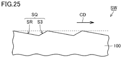
- Surface SW of p type body layer 122 ( Fig. 4 ) forming the channel surface is preferably a surface having a special plane. As shown in Fig. 18 , such surface SW includes a plane S1 (first plane) having a plane orientation of ⁇ 0-33-8 ⁇ . Plane S1 preferably has a plane orientation of (0-33-8).
- surface SW includes plane S1 microscopically, and further includes a plane S2 (second plane) having a plane orientation of ⁇ 0-11-1 ⁇ microscopically.
- plane S2 second plane
- the term "microscopically” as used herein means “minutely to such an extent that at least the size about twice as large as an interatomic spacing is considered.”
- a TEM Transmission Electron Microscope
- Plane S2 preferably has a plane orientation of (0-11-1).
- plane S1 and plane S2 of surface SW form a combined plane SR having a plane orientation of ⁇ 0-11-2 ⁇ . That is, combined plane SR is formed of periodically repeated planes S1 and S2. Such a periodic structure can be observed, for example, by TEM or AFM (Atomic Force Microscopy).
- combined plane SR macroscopically has an off angle of 62° relative to the ⁇ 000-1 ⁇ plane.
- the term "macroscopically” as used herein means "disregarding a fine structure having a size of approximately interatomic spacing.” For the measurement of such a macroscopic off angle, a method employing general X-ray diffraction can be used, for example.
- combined plane SR has a plane orientation of (0-11-2). In this case, combined plane SR macroscopically has an off angle of 62° relative to the (000-1) plane.
- channels in which the above-described periodic repetition is done.
- Si atoms (or C atoms)
- a silicon carbide single crystal of polytype 4H is viewed from the (000-1) plane
- atoms in a layer A solid line in the figure
- atoms in a layer B broken line in the figure
- atoms in a layer C chain-dotted line in the figure
- atoms in a layer B (not shown) disposed therebelow
- atoms in a layer B (not shown) disposed therebelow
- a periodic stacking structure such as ABCBABCBABCB ... is provided.
- combined plane SR is formed by alternately providing planes S1 having a plane orientation of (0-33-8) and planes S2 connected to planes S1 and having a plane orientation different from that of planes S1
- Each of planes S1 and S2 has a length twice as large as the interatomic spacing of the Si atoms (or C atoms). It is noted that a plane with plane S1 and plane S2 being averaged corresponds to the (0-11-2) plane ( Fig. 20 ).
- the single-crystal structure has a portion periodically including a structure (the portion of plane S1) equivalent to a cubic structure.
- combined plane SR is formed by alternately providing planes S1 having a plane orientation of (001) in the above-described structure equivalent to a cubic structure and planes S2 connected to planes S1 and having a plane orientation different from that of planes S1.
- the surface can be thus formed of the planes (planes S1 in Fig. 22 ) having a plane orientation of (001) in the structure equivalent to a cubic structure and the planes (planes S2 in Fig. 22 ) connected to the foregoing planes and having a plane orientation different from that of the foregoing planes.
- the polytype may be 6H or 15R, for example.
- Fig. 23 relation between the crystal plane of surface SW and mobility MB in the channel surface is described.
- the horizontal axis represents an angle D1 formed by the (000-1) plane and the macroscopic plane orientation of surface SW having the channel surface
- the vertical axis represents mobility MB.
- a group of plots CM corresponds to a case where surface SW is finished to have the special plane through thermal etching
- a group of plots MC corresponds to a case where surface SW is not subjected to such thermal etching.
- mobility MB is at maximum when the surface of the channel surface has a macroscopic plane orientation of (0-33-8). This is presumably due to the following reason. That is, in the case where the thermal etching is not performed, i.e., in the case where the microscopic structure of the channel surface is not particularly controlled, the macroscopic plane orientation thereof corresponds to (0-33-8), with the result that a ratio of the microscopic plane orientation of (0-33-8), i.e., the plane orientation of (0-33-8) in consideration of that in atomic level, becomes statistically high.
- mobility MB in group of plots CM is at maximum when the macroscopic plane orientation of the surface of the channel surface is (0-11-2) (arrow EX).
- This is presumably due to the following reason. That is, as shown in Figs. 21 and 22 , the large number of planes S1 each having a plane orientation of (0-33-8) are densely and regularly arranged with planes S2 interposed therebetween, whereby a ratio of the microscopic plane orientation of (0-33-8) becomes high in the surface of the channel surface.
- mobility MB has orientation dependency on combined plane SR.
- the horizontal axis represents an angle D2 between the channel direction and the ⁇ 0-11-2> direction
- the vertical axis represents mobility MB (in any unit) in the channel surface.
- a broken line is supplementarily provided therein for viewability of the graph. It has been found from this graph that in order to increase channel mobility MB, channel direction CD ( Fig. 18 ) preferably has an angle D2 of not less than 0° and not more than 60°, and more preferably, substantially 0°.
- surface SW may further include a plane S3 (third plane) in addition to combined plane SR. More specifically, surface SW may include a combined plane SQ formed of periodically repeated planes S3 and combined planes SR.
- the off angle of surface SW relative to the ⁇ 000-1 ⁇ plane is deviated from the ideal off angle of combined plane SR, i.e., 62°. This deviation is preferably small, and preferably in a range of ⁇ 10°. Examples of a surface included in such an angle range include a surface having a macroscopic plane orientation of the ⁇ 0-33-8 ⁇ plane.
- the off angle of surface SW relative to the (000-1) plane is deviated from the ideal off angle of combined plane SR, i.e., 62°.
- This deviation is preferably small, and preferably in a range of ⁇ 10°.
- Examples of a surface included in such an angle range include a surface having a macroscopic plane orientation of the (0-33-8) plane.
- Such a periodic structure can be observed, for example, by TEM or AFM.
Landscapes
- Recrystallisation Techniques (AREA)
- Insulated Gate Type Field-Effect Transistor (AREA)
- Electrodes Of Semiconductors (AREA)
- Physics & Mathematics (AREA)
- Engineering & Computer Science (AREA)
- Plasma & Fusion (AREA)
Claims (8)
- Siliziumkarbid-Halbleitervorrichtung, umfassend:ein Siliziumkarbidsubstrat (100), das eine erste Schicht (121) mit einem ersten Leitfähigkeitstyp, eine zweite Schicht (122) mit einem zweiten Leitfähigkeitstyp, die auf der ersten Schicht vorgesehen ist, und eine dritte Schicht (123), die auf der zweiten Schicht vorgesehen ist und mit einer Verunreinigung zur Bildung des ersten Leitfähigkeitstyps dotiert ist, umfasst,wobei das Siliziumkarbidsubstrat einen Graben (TR) aufweist, der durch die dritte Schicht (123) und die zweite Schicht (122) gebildet ist, um die erste Schicht (121) zu erreichen, wobei die erste Schicht (121) einen Verunreinigungskonzentrationshöchstwert des ersten Leitfähigkeitstyps an einer Position entfernt von dem Graben (TR) in der ersten Schicht (121) aufweist;eine Gate-Isolierfolie (203), die den Graben (TR) bedeckt; undeine Gate-Elektrode (202), die auf dem Gate-Isolierfilm (203) vorgesehen ist, wobei die Gate-Elektrode (202) einer Fläche der zweiten Schicht zugewandt ist, wobei der Gate-Isolierfilm dazwischen angeordnet ist,dadurch gekennzeichnet, dassdie zweite Schicht (122) einen Konzentrationshöchstwert der Verunreinigung, die den Konzentrationshöchstwert in der ersten Schicht aufweist, an einer Position entfernt vom Graben (TR) in der zweiten Schicht (122) aufweist.
- Siliziumkarbid-Halbleitervorrichtung nach Anspruch 1, wobei
die Verunreinigungskonzentration in der ersten Schicht am Boden des Grabens nicht mehr als 110% eines Mindestwertes der Verunreinigungskonzentration in der ersten Schicht beträgt. - Siliziumkarbid-Halbleitervorrichtung nach Anspruch 1 oder 2, wobei
am Boden des Grabens ein Profil des Verunreinigungskonzentrationshöchstwerts eine Dosis von nicht weniger als 1 × 10¹¹/cm2 aufweist, die erhalten wird, indem eine Datenverarbeitung zum Entfernen eines Hintergrunds am Profil des Konzentrationshöchstwerts durchgeführt und anschließend dieses in Richtung der Dicke der ersten, zweiten und dritten Schicht integriert wird. - Siliziumkarbid-Halbleitervorrichtung nach einem der Ansprüche 1 bis 3, wobei das Siliziumkarbidsubstrat aus Siliziumkarbid mit einer hexagonalen Kristallstruktur mit dem Polytyp 4H hergestellt ist.
- Siliziumkarbid-Halbleitervorrichtung nach Anspruch 4, wobei die Oberfläche der zweiten Schicht eine erste Ebene mit einer {0-33-8} Ebenenausrichtung umfasst.
- Siliziumkarbid-Halbleitervorrichtung nach Anspruch 5, wobei die Oberfläche mikroskopisch die erste Ebene umfasst und ferner mikroskopisch eine zweite Ebene mit einer {0-11-1} Ebenenausrichtung umfasst.
- Siliziumkarbid-Halbleitervorrichtung nach Anspruch 6, wobei die erste und zweite Ebene der Oberfläche eine kombinierte Ebene mit einer {0-11-2} Ebenenausrichtung bilden.
- Siliziumkarbid-Halbleitervorrichtung nach Anspruch 7, wobei die Oberfläche makroskopisch einen Versatzwinkel von 62°±10° relativ zur {000-1} Ebene aufweist.
Applications Claiming Priority (2)
| Application Number | Priority Date | Filing Date | Title |
|---|---|---|---|
| JP2012113939A JP2013243179A (ja) | 2012-05-18 | 2012-05-18 | 炭化珪素半導体装置 |
| PCT/JP2013/060608 WO2013172124A1 (ja) | 2012-05-18 | 2013-04-08 | 炭化珪素半導体装置 |
Publications (3)
| Publication Number | Publication Date |
|---|---|
| EP2851957A1 EP2851957A1 (de) | 2015-03-25 |
| EP2851957A4 EP2851957A4 (de) | 2016-01-06 |
| EP2851957B1 true EP2851957B1 (de) | 2019-09-25 |
Family
ID=49580587
Family Applications (1)
| Application Number | Title | Priority Date | Filing Date |
|---|---|---|---|
| EP13790103.9A Active EP2851957B1 (de) | 2012-05-18 | 2013-04-08 | Halbleiterbauelement aus siliciumcarbid |
Country Status (5)
| Country | Link |
|---|---|
| US (1) | US8878192B2 (de) |
| EP (1) | EP2851957B1 (de) |
| JP (1) | JP2013243179A (de) |
| CN (1) | CN104205339B (de) |
| WO (1) | WO2013172124A1 (de) |
Families Citing this family (4)
| Publication number | Priority date | Publication date | Assignee | Title |
|---|---|---|---|---|
| US9748341B2 (en) * | 2013-07-02 | 2017-08-29 | General Electric Company | Metal-oxide-semiconductor (MOS) devices with increased channel periphery |
| JP2016213419A (ja) * | 2015-05-13 | 2016-12-15 | 住友電気工業株式会社 | 炭化珪素半導体装置 |
| CN114503283B (zh) * | 2019-12-20 | 2025-11-25 | 住友电气工业株式会社 | 碳化硅半导体装置 |
| CN111276545B (zh) * | 2020-02-12 | 2023-03-14 | 重庆伟特森电子科技有限公司 | 一种新型沟槽碳化硅晶体管器件及其制作方法 |
Family Cites Families (16)
| Publication number | Priority date | Publication date | Assignee | Title |
|---|---|---|---|---|
| US5506421A (en) * | 1992-11-24 | 1996-04-09 | Cree Research, Inc. | Power MOSFET in silicon carbide |
| US5939752A (en) * | 1995-12-12 | 1999-08-17 | Siliconix Incorporated | Low voltage MOSFET with low on-resistance and high breakdown voltage |
| DE69739206D1 (de) * | 1996-07-19 | 2009-02-26 | Siliconix Inc | Hochdichte-graben-dmos-transistor mit grabenbodemimplantierung |
| JPH11177086A (ja) * | 1997-12-09 | 1999-07-02 | Hitachi Ltd | 縦型電界効果トランジスタとその製造方法 |
| US6262453B1 (en) * | 1998-04-24 | 2001-07-17 | Magepower Semiconductor Corp. | Double gate-oxide for reducing gate-drain capacitance in trenched DMOS with high-dopant concentration buried-region under trenched gate |
| JP3954541B2 (ja) * | 2003-08-05 | 2007-08-08 | 株式会社東芝 | 半導体装置及びその製造方法 |
| JP2007299861A (ja) | 2006-04-28 | 2007-11-15 | Nissan Motor Co Ltd | 半導体装置 |
| US8198675B2 (en) | 2006-11-21 | 2012-06-12 | Sumitomo Electric Industries, Ltd. | Silicon carbide semiconductor device and method of manufacturing the same |
| JP4450241B2 (ja) * | 2007-03-20 | 2010-04-14 | 株式会社デンソー | 炭化珪素半導体装置の製造方法 |
| JP5233158B2 (ja) | 2007-04-25 | 2013-07-10 | 富士電機株式会社 | 炭化珪素半導体装置 |
| JP2009094203A (ja) * | 2007-10-05 | 2009-04-30 | Denso Corp | 炭化珪素半導体装置 |
| JP4798119B2 (ja) | 2007-11-06 | 2011-10-19 | 株式会社デンソー | 炭化珪素半導体装置およびその製造方法 |
| JP5157843B2 (ja) * | 2007-12-04 | 2013-03-06 | 住友電気工業株式会社 | 炭化ケイ素半導体装置およびその製造方法 |
| US20090315104A1 (en) * | 2008-06-20 | 2009-12-24 | Force Mos Technology Co. Ltd. | Trench MOSFET with shallow trench structures |
| JP2012038771A (ja) * | 2010-08-03 | 2012-02-23 | Sumitomo Electric Ind Ltd | 半導体装置およびその製造方法 |
| JP5741583B2 (ja) * | 2010-08-03 | 2015-07-01 | 住友電気工業株式会社 | 半導体装置およびその製造方法 |
-
2012
- 2012-05-18 JP JP2012113939A patent/JP2013243179A/ja active Pending
-
2013
- 2013-04-08 CN CN201380017424.2A patent/CN104205339B/zh not_active Expired - Fee Related
- 2013-04-08 EP EP13790103.9A patent/EP2851957B1/de active Active
- 2013-04-08 WO PCT/JP2013/060608 patent/WO2013172124A1/ja not_active Ceased
- 2013-04-15 US US13/863,043 patent/US8878192B2/en not_active Expired - Fee Related
Non-Patent Citations (1)
| Title |
|---|
| None * |
Also Published As
| Publication number | Publication date |
|---|---|
| US20130306986A1 (en) | 2013-11-21 |
| CN104205339B (zh) | 2017-02-22 |
| CN104205339A (zh) | 2014-12-10 |
| EP2851957A4 (de) | 2016-01-06 |
| JP2013243179A (ja) | 2013-12-05 |
| WO2013172124A1 (ja) | 2013-11-21 |
| EP2851957A1 (de) | 2015-03-25 |
| US8878192B2 (en) | 2014-11-04 |
Similar Documents
| Publication | Publication Date | Title |
|---|---|---|
| US8803252B2 (en) | Silicon carbide semiconductor device | |
| EP2602824B1 (de) | Verfahren zur herstellung von halbleiterbauelementen | |
| US8952393B2 (en) | Silicon carbide semiconductor device | |
| US9276106B2 (en) | Silicon carbide semiconductor device and method for manufacturing same | |
| EP2763180B1 (de) | Halbleiterbauelement aus siliciumcarbid | |
| US9647106B2 (en) | Silicon carbide semiconductor device and method for manufacturing same | |
| US9627487B2 (en) | Method for manufacturing silicon carbide semiconductor device and silicon carbide semiconductor device | |
| JP6171678B2 (ja) | 炭化珪素半導体装置およびその製造方法 | |
| US20160126347A1 (en) | Silicon carbide semiconductor device | |
| US20150279967A1 (en) | Method for manufacturing silicon carbide semiconductor device | |
| EP2851957B1 (de) | Halbleiterbauelement aus siliciumcarbid | |
| US8927368B2 (en) | Method for manufacturing silicon carbide semiconductor device | |
| US20160293690A1 (en) | Silicon carbide semiconductor device and method for manufacturing same | |
| EP2866265A1 (de) | Verfahren zur herstellung eines siliciumcarbidhalbleiterbauelements und siliciumcarbidhalbleiterbauelement | |
| US9679986B2 (en) | Silicon carbide semiconductor device | |
| US9793365B2 (en) | Method for manufacturing silicon carbide semiconductor device having trench | |
| US20130306987A1 (en) | Silicon carbide semiconductor device and method for manufacturing same |
Legal Events
| Date | Code | Title | Description |
|---|---|---|---|
| PUAI | Public reference made under article 153(3) epc to a published international application that has entered the european phase |
Free format text: ORIGINAL CODE: 0009012 |
|
| 17P | Request for examination filed |
Effective date: 20141017 |
|
| AK | Designated contracting states |
Kind code of ref document: A1 Designated state(s): AL AT BE BG CH CY CZ DE DK EE ES FI FR GB GR HR HU IE IS IT LI LT LU LV MC MK MT NL NO PL PT RO RS SE SI SK SM TR |
|
| AX | Request for extension of the european patent |
Extension state: BA ME |
|
| DAX | Request for extension of the european patent (deleted) | ||
| RA4 | Supplementary search report drawn up and despatched (corrected) |
Effective date: 20151209 |
|
| RIC1 | Information provided on ipc code assigned before grant |
Ipc: H01L 29/78 20060101AFI20151203BHEP Ipc: H01L 21/336 20060101ALI20151203BHEP Ipc: H01L 29/12 20060101ALI20151203BHEP |
|
| RIN1 | Information on inventor provided before grant (corrected) |
Inventor name: WADA, KEIJI Inventor name: MASUDA, TAKEYOSHI Inventor name: HIYOSHI, TORU |
|
| GRAP | Despatch of communication of intention to grant a patent |
Free format text: ORIGINAL CODE: EPIDOSNIGR1 |
|
| STAA | Information on the status of an ep patent application or granted ep patent |
Free format text: STATUS: GRANT OF PATENT IS INTENDED |
|
| INTG | Intention to grant announced |
Effective date: 20190412 |
|
| GRAS | Grant fee paid |
Free format text: ORIGINAL CODE: EPIDOSNIGR3 |
|
| GRAA | (expected) grant |
Free format text: ORIGINAL CODE: 0009210 |
|
| STAA | Information on the status of an ep patent application or granted ep patent |
Free format text: STATUS: THE PATENT HAS BEEN GRANTED |
|
| AK | Designated contracting states |
Kind code of ref document: B1 Designated state(s): AL AT BE BG CH CY CZ DE DK EE ES FI FR GB GR HR HU IE IS IT LI LT LU LV MC MK MT NL NO PL PT RO RS SE SI SK SM TR |
|
| REG | Reference to a national code |
Ref country code: GB Ref legal event code: FG4D |
|
| REG | Reference to a national code |
Ref country code: CH Ref legal event code: EP |
|
| REG | Reference to a national code |
Ref country code: AT Ref legal event code: REF Ref document number: 1184680 Country of ref document: AT Kind code of ref document: T Effective date: 20191015 |
|
| REG | Reference to a national code |
Ref country code: IE Ref legal event code: FG4D |
|
| REG | Reference to a national code |
Ref country code: DE Ref legal event code: R096 Ref document number: 602013061000 Country of ref document: DE |
|
| REG | Reference to a national code |
Ref country code: NL Ref legal event code: MP Effective date: 20190925 |
|
| PG25 | Lapsed in a contracting state [announced via postgrant information from national office to epo] |
Ref country code: FI Free format text: LAPSE BECAUSE OF FAILURE TO SUBMIT A TRANSLATION OF THE DESCRIPTION OR TO PAY THE FEE WITHIN THE PRESCRIBED TIME-LIMIT Effective date: 20190925 Ref country code: LT Free format text: LAPSE BECAUSE OF FAILURE TO SUBMIT A TRANSLATION OF THE DESCRIPTION OR TO PAY THE FEE WITHIN THE PRESCRIBED TIME-LIMIT Effective date: 20190925 Ref country code: BG Free format text: LAPSE BECAUSE OF FAILURE TO SUBMIT A TRANSLATION OF THE DESCRIPTION OR TO PAY THE FEE WITHIN THE PRESCRIBED TIME-LIMIT Effective date: 20191225 Ref country code: NO Free format text: LAPSE BECAUSE OF FAILURE TO SUBMIT A TRANSLATION OF THE DESCRIPTION OR TO PAY THE FEE WITHIN THE PRESCRIBED TIME-LIMIT Effective date: 20191225 Ref country code: SE Free format text: LAPSE BECAUSE OF FAILURE TO SUBMIT A TRANSLATION OF THE DESCRIPTION OR TO PAY THE FEE WITHIN THE PRESCRIBED TIME-LIMIT Effective date: 20190925 Ref country code: HR Free format text: LAPSE BECAUSE OF FAILURE TO SUBMIT A TRANSLATION OF THE DESCRIPTION OR TO PAY THE FEE WITHIN THE PRESCRIBED TIME-LIMIT Effective date: 20190925 |
|
| REG | Reference to a national code |
Ref country code: LT Ref legal event code: MG4D |
|
| PG25 | Lapsed in a contracting state [announced via postgrant information from national office to epo] |
Ref country code: LV Free format text: LAPSE BECAUSE OF FAILURE TO SUBMIT A TRANSLATION OF THE DESCRIPTION OR TO PAY THE FEE WITHIN THE PRESCRIBED TIME-LIMIT Effective date: 20190925 Ref country code: GR Free format text: LAPSE BECAUSE OF FAILURE TO SUBMIT A TRANSLATION OF THE DESCRIPTION OR TO PAY THE FEE WITHIN THE PRESCRIBED TIME-LIMIT Effective date: 20191226 Ref country code: RS Free format text: LAPSE BECAUSE OF FAILURE TO SUBMIT A TRANSLATION OF THE DESCRIPTION OR TO PAY THE FEE WITHIN THE PRESCRIBED TIME-LIMIT Effective date: 20190925 |
|
| REG | Reference to a national code |
Ref country code: AT Ref legal event code: MK05 Ref document number: 1184680 Country of ref document: AT Kind code of ref document: T Effective date: 20190925 |
|
| PG25 | Lapsed in a contracting state [announced via postgrant information from national office to epo] |
Ref country code: EE Free format text: LAPSE BECAUSE OF FAILURE TO SUBMIT A TRANSLATION OF THE DESCRIPTION OR TO PAY THE FEE WITHIN THE PRESCRIBED TIME-LIMIT Effective date: 20190925 Ref country code: PL Free format text: LAPSE BECAUSE OF FAILURE TO SUBMIT A TRANSLATION OF THE DESCRIPTION OR TO PAY THE FEE WITHIN THE PRESCRIBED TIME-LIMIT Effective date: 20190925 Ref country code: AT Free format text: LAPSE BECAUSE OF FAILURE TO SUBMIT A TRANSLATION OF THE DESCRIPTION OR TO PAY THE FEE WITHIN THE PRESCRIBED TIME-LIMIT Effective date: 20190925 Ref country code: AL Free format text: LAPSE BECAUSE OF FAILURE TO SUBMIT A TRANSLATION OF THE DESCRIPTION OR TO PAY THE FEE WITHIN THE PRESCRIBED TIME-LIMIT Effective date: 20190925 Ref country code: PT Free format text: LAPSE BECAUSE OF FAILURE TO SUBMIT A TRANSLATION OF THE DESCRIPTION OR TO PAY THE FEE WITHIN THE PRESCRIBED TIME-LIMIT Effective date: 20200127 Ref country code: IT Free format text: LAPSE BECAUSE OF FAILURE TO SUBMIT A TRANSLATION OF THE DESCRIPTION OR TO PAY THE FEE WITHIN THE PRESCRIBED TIME-LIMIT Effective date: 20190925 Ref country code: ES Free format text: LAPSE BECAUSE OF FAILURE TO SUBMIT A TRANSLATION OF THE DESCRIPTION OR TO PAY THE FEE WITHIN THE PRESCRIBED TIME-LIMIT Effective date: 20190925 Ref country code: RO Free format text: LAPSE BECAUSE OF FAILURE TO SUBMIT A TRANSLATION OF THE DESCRIPTION OR TO PAY THE FEE WITHIN THE PRESCRIBED TIME-LIMIT Effective date: 20190925 Ref country code: NL Free format text: LAPSE BECAUSE OF FAILURE TO SUBMIT A TRANSLATION OF THE DESCRIPTION OR TO PAY THE FEE WITHIN THE PRESCRIBED TIME-LIMIT Effective date: 20190925 |
|
| PG25 | Lapsed in a contracting state [announced via postgrant information from national office to epo] |
Ref country code: SM Free format text: LAPSE BECAUSE OF FAILURE TO SUBMIT A TRANSLATION OF THE DESCRIPTION OR TO PAY THE FEE WITHIN THE PRESCRIBED TIME-LIMIT Effective date: 20190925 Ref country code: SK Free format text: LAPSE BECAUSE OF FAILURE TO SUBMIT A TRANSLATION OF THE DESCRIPTION OR TO PAY THE FEE WITHIN THE PRESCRIBED TIME-LIMIT Effective date: 20190925 Ref country code: CZ Free format text: LAPSE BECAUSE OF FAILURE TO SUBMIT A TRANSLATION OF THE DESCRIPTION OR TO PAY THE FEE WITHIN THE PRESCRIBED TIME-LIMIT Effective date: 20190925 Ref country code: IS Free format text: LAPSE BECAUSE OF FAILURE TO SUBMIT A TRANSLATION OF THE DESCRIPTION OR TO PAY THE FEE WITHIN THE PRESCRIBED TIME-LIMIT Effective date: 20200224 |
|
| REG | Reference to a national code |
Ref country code: DE Ref legal event code: R097 Ref document number: 602013061000 Country of ref document: DE |
|
| PG2D | Information on lapse in contracting state deleted |
Ref country code: IS |
|
| PG25 | Lapsed in a contracting state [announced via postgrant information from national office to epo] |
Ref country code: DK Free format text: LAPSE BECAUSE OF FAILURE TO SUBMIT A TRANSLATION OF THE DESCRIPTION OR TO PAY THE FEE WITHIN THE PRESCRIBED TIME-LIMIT Effective date: 20190925 Ref country code: IS Free format text: LAPSE BECAUSE OF FAILURE TO SUBMIT A TRANSLATION OF THE DESCRIPTION OR TO PAY THE FEE WITHIN THE PRESCRIBED TIME-LIMIT Effective date: 20200126 |
|
| PLBE | No opposition filed within time limit |
Free format text: ORIGINAL CODE: 0009261 |
|
| STAA | Information on the status of an ep patent application or granted ep patent |
Free format text: STATUS: NO OPPOSITION FILED WITHIN TIME LIMIT |
|
| 26N | No opposition filed |
Effective date: 20200626 |
|
| PG25 | Lapsed in a contracting state [announced via postgrant information from national office to epo] |
Ref country code: MC Free format text: LAPSE BECAUSE OF FAILURE TO SUBMIT A TRANSLATION OF THE DESCRIPTION OR TO PAY THE FEE WITHIN THE PRESCRIBED TIME-LIMIT Effective date: 20190925 Ref country code: SI Free format text: LAPSE BECAUSE OF FAILURE TO SUBMIT A TRANSLATION OF THE DESCRIPTION OR TO PAY THE FEE WITHIN THE PRESCRIBED TIME-LIMIT Effective date: 20190925 |
|
| REG | Reference to a national code |
Ref country code: CH Ref legal event code: PL |
|
| PG25 | Lapsed in a contracting state [announced via postgrant information from national office to epo] |
Ref country code: CH Free format text: LAPSE BECAUSE OF NON-PAYMENT OF DUE FEES Effective date: 20200430 Ref country code: LI Free format text: LAPSE BECAUSE OF NON-PAYMENT OF DUE FEES Effective date: 20200430 Ref country code: FR Free format text: LAPSE BECAUSE OF NON-PAYMENT OF DUE FEES Effective date: 20200430 Ref country code: LU Free format text: LAPSE BECAUSE OF NON-PAYMENT OF DUE FEES Effective date: 20200408 |
|
| REG | Reference to a national code |
Ref country code: BE Ref legal event code: MM Effective date: 20200430 |
|
| PG25 | Lapsed in a contracting state [announced via postgrant information from national office to epo] |
Ref country code: BE Free format text: LAPSE BECAUSE OF NON-PAYMENT OF DUE FEES Effective date: 20200430 |
|
| GBPC | Gb: european patent ceased through non-payment of renewal fee |
Effective date: 20200408 |
|
| PG25 | Lapsed in a contracting state [announced via postgrant information from national office to epo] |
Ref country code: GB Free format text: LAPSE BECAUSE OF NON-PAYMENT OF DUE FEES Effective date: 20200408 Ref country code: IE Free format text: LAPSE BECAUSE OF NON-PAYMENT OF DUE FEES Effective date: 20200408 |
|
| PG25 | Lapsed in a contracting state [announced via postgrant information from national office to epo] |
Ref country code: TR Free format text: LAPSE BECAUSE OF FAILURE TO SUBMIT A TRANSLATION OF THE DESCRIPTION OR TO PAY THE FEE WITHIN THE PRESCRIBED TIME-LIMIT Effective date: 20190925 Ref country code: MT Free format text: LAPSE BECAUSE OF FAILURE TO SUBMIT A TRANSLATION OF THE DESCRIPTION OR TO PAY THE FEE WITHIN THE PRESCRIBED TIME-LIMIT Effective date: 20190925 Ref country code: CY Free format text: LAPSE BECAUSE OF FAILURE TO SUBMIT A TRANSLATION OF THE DESCRIPTION OR TO PAY THE FEE WITHIN THE PRESCRIBED TIME-LIMIT Effective date: 20190925 |
|
| PG25 | Lapsed in a contracting state [announced via postgrant information from national office to epo] |
Ref country code: MK Free format text: LAPSE BECAUSE OF FAILURE TO SUBMIT A TRANSLATION OF THE DESCRIPTION OR TO PAY THE FEE WITHIN THE PRESCRIBED TIME-LIMIT Effective date: 20190925 |
|
| PGFP | Annual fee paid to national office [announced via postgrant information from national office to epo] |
Ref country code: DE Payment date: 20220302 Year of fee payment: 10 |
|
| REG | Reference to a national code |
Ref country code: DE Ref legal event code: R119 Ref document number: 602013061000 Country of ref document: DE |
|
| PG25 | Lapsed in a contracting state [announced via postgrant information from national office to epo] |
Ref country code: DE Free format text: LAPSE BECAUSE OF NON-PAYMENT OF DUE FEES Effective date: 20231103 |