EP2851970B1 - Leuchtdioden-Halbleiterbauelement - Google Patents
Leuchtdioden-Halbleiterbauelement Download PDFInfo
- Publication number
- EP2851970B1 EP2851970B1 EP14180009.4A EP14180009A EP2851970B1 EP 2851970 B1 EP2851970 B1 EP 2851970B1 EP 14180009 A EP14180009 A EP 14180009A EP 2851970 B1 EP2851970 B1 EP 2851970B1
- Authority
- EP
- European Patent Office
- Prior art keywords
- electrode
- layer
- conversion
- light emitting
- semiconductor layer
- Prior art date
- Legal status (The legal status is an assumption and is not a legal conclusion. Google has not performed a legal analysis and makes no representation as to the accuracy of the status listed.)
- Active
Links
Images



Classifications
-
- H—ELECTRICITY
- H10—SEMICONDUCTOR DEVICES; ELECTRIC SOLID-STATE DEVICES NOT OTHERWISE PROVIDED FOR
- H10H—INORGANIC LIGHT-EMITTING SEMICONDUCTOR DEVICES HAVING POTENTIAL BARRIERS
- H10H20/00—Individual inorganic light-emitting semiconductor devices having potential barriers, e.g. light-emitting diodes [LED]
- H10H20/80—Constructional details
- H10H20/81—Bodies
- H10H20/814—Bodies having reflecting means, e.g. semiconductor Bragg reflectors
-
- H—ELECTRICITY
- H10—SEMICONDUCTOR DEVICES; ELECTRIC SOLID-STATE DEVICES NOT OTHERWISE PROVIDED FOR
- H10H—INORGANIC LIGHT-EMITTING SEMICONDUCTOR DEVICES HAVING POTENTIAL BARRIERS
- H10H20/00—Individual inorganic light-emitting semiconductor devices having potential barriers, e.g. light-emitting diodes [LED]
- H10H20/80—Constructional details
- H10H20/83—Electrodes
- H10H20/831—Electrodes characterised by their shape
- H10H20/8314—Electrodes characterised by their shape extending at least partially onto an outer side surface of the bodies
-
- H—ELECTRICITY
- H10—SEMICONDUCTOR DEVICES; ELECTRIC SOLID-STATE DEVICES NOT OTHERWISE PROVIDED FOR
- H10H—INORGANIC LIGHT-EMITTING SEMICONDUCTOR DEVICES HAVING POTENTIAL BARRIERS
- H10H20/00—Individual inorganic light-emitting semiconductor devices having potential barriers, e.g. light-emitting diodes [LED]
- H10H20/80—Constructional details
- H10H20/83—Electrodes
- H10H20/832—Electrodes characterised by their material
- H10H20/833—Transparent materials
-
- H—ELECTRICITY
- H10—SEMICONDUCTOR DEVICES; ELECTRIC SOLID-STATE DEVICES NOT OTHERWISE PROVIDED FOR
- H10H—INORGANIC LIGHT-EMITTING SEMICONDUCTOR DEVICES HAVING POTENTIAL BARRIERS
- H10H20/00—Individual inorganic light-emitting semiconductor devices having potential barriers, e.g. light-emitting diodes [LED]
- H10H20/80—Constructional details
- H10H20/83—Electrodes
- H10H20/832—Electrodes characterised by their material
- H10H20/835—Reflective materials
-
- H—ELECTRICITY
- H10—SEMICONDUCTOR DEVICES; ELECTRIC SOLID-STATE DEVICES NOT OTHERWISE PROVIDED FOR
- H10H—INORGANIC LIGHT-EMITTING SEMICONDUCTOR DEVICES HAVING POTENTIAL BARRIERS
- H10H20/00—Individual inorganic light-emitting semiconductor devices having potential barriers, e.g. light-emitting diodes [LED]
- H10H20/80—Constructional details
- H10H20/85—Packages
- H10H20/851—Wavelength conversion means
- H10H20/8511—Wavelength conversion means characterised by their material, e.g. binder
- H10H20/8512—Wavelength conversion materials
-
- H—ELECTRICITY
- H10—SEMICONDUCTOR DEVICES; ELECTRIC SOLID-STATE DEVICES NOT OTHERWISE PROVIDED FOR
- H10H—INORGANIC LIGHT-EMITTING SEMICONDUCTOR DEVICES HAVING POTENTIAL BARRIERS
- H10H20/00—Individual inorganic light-emitting semiconductor devices having potential barriers, e.g. light-emitting diodes [LED]
- H10H20/80—Constructional details
- H10H20/85—Packages
- H10H20/857—Interconnections, e.g. lead-frames, bond wires or solder balls
Definitions
- Embodiments described herein relate generally to a semiconductor light emitting diode device, in the following called light emitting device.
- a lighting apparatus is being developed using a semiconductor light emitting element such as an LED (light emitting diode).
- a semiconductor light emitting device that emits white light can be formed by combining a nitride semiconductor LED that emits blue light and a fluorescent substance that absorbs blue light and emits yellow-based light. In such a semiconductor light emitting device, it is important to enhance the extraction efficiency of light emitted from a light emitting layer.
- a semiconductor light emitting diode device is defined according to claim 1.
- Various embodiments will be described hereinafter with reference to the accompanying drawings. Identical components in the drawings are marked with the same reference numerals, and a detailed description thereof is omitted as appropriate and different components are described.
- the drawings are schematic or conceptual; and the relationships between the thickness and width of portions, the proportions of sizes among portions, etc. are not necessarily the same as the actual values thereof. Further, the dimensions and proportions may be illustrated differently among drawings, even for identical portions.
- FIG. 1A and FIG. 1B are schematic views illustrating a semiconductor light emitting device 100 according to an embodiment.
- FIG. 1A is a plan view
- FIG. 1B is a cross-sectional view taken along line A-A of FIG. 1A .
- the semiconductor light emitting device 100 includes a stacked body 15, a first electrode 40, a second electrode 50, a first conversion electrode 43, a second conversion electrode 53, a light blocking body 57, a first pillar 45, a second pillar 55, and a sealing body 80.
- the stacked body 15 includes a first semiconductor layer 10 of a first conductivity type, a second semiconductor layer 20 of a second conductivity type, and a light emitting layer 30.
- the stacked body 15 has a first portion 15a and a second portion 15b.
- the first portion 15a includes a part of the first semiconductor layer 10, the second semiconductor layer 20, and the light emitting layer 30 provided between the part of the first semiconductor layer 10 and the second semiconductor layer 20.
- the second portion 15b includes a rest part of the first semiconductor layer 10.
- the first conductivity type is an n-type, for example, and the second conductivity type is a p-type different from the first conductivity type.
- the embodiment is not limited thereto, and the p-type may be taken as the first conductivity type and the n-type may be taken as the second conductivity type.
- the first semiconductor layer 10, the second semiconductor layer 20, and the light emitting layer 30 include a nitride semiconductor, for example.
- the first semiconductor layer 10 includes an n-type cladding layer, for example.
- the second semiconductor layer 20 includes a p-type cladding layer, for example.
- the light emitting layer 30 includes, for example, a quantum well in which nitride semiconductors of different compositions are stacked.
- the stacked body 15 has, for example, a first surface 15f and a second surface 15g on the opposite side to the first surface 15f.
- the first surface 15f is a surface of the first semiconductor layer 10 on the opposite side to the light emitting layer 30.
- the second surface 15g is a surface of the second semiconductor layer 20 on the opposite side to the light emitting layer 30.
- a direction from the first semiconductor layer 10 toward the second semiconductor layer 20 is defined as a Z-axis direction (a first direction).
- One axis perpendicular to the Z-axis is defined as an X-axis (a second axis).
- the axis perpendicular to the Z-axis and the X-axis is defined as a Y-axis (referred to as a third axis).
- the Z-axis (a first axis) is perpendicular to the first surface 15f and is perpendicular to the second surface 15g.
- the first semiconductor layer 10, the light emitting layer 30, and the second semiconductor layer 20 are formed in this order on a substrate by crystal growth to form the stacked body 15. Then, a part of the stacked body 15 is removed from the second surface 15g side until reaching the first semiconductor layer 10. Thereby, a part of the first semiconductor layer 10 (the second portion 15b) is exposed. The light emitting layer 30 and the second semiconductor layer 20 are left in the first portion 15a. Thus, the second portion 15b is juxtaposed to the first portion 15a in the X-Y plane.
- the first electrode 40 is provided on the second surface 15g side of the second semiconductor layer 20.
- the first electrode 40 includes a p-side electrode 41 and a p-side conductive layer 42.
- the p-side conductive layer 42 is provided on the second semiconductor layer 20 on the second surface 15g side. A part of the p-side conductive layer 42 is provided between the p-side electrode 41 and the second semiconductor layer 20.
- the second electrode 50 is provided on a surface of the second portion 15b of the stacked body 15 on the second surface 15g side. That is, the second electrode 50 is provided on the part of the first semiconductor layer mentioned above, which is exposed.
- the embodiment is not limited thereto, and the p-side conductive layer 42 may not be provided in the first electrode 40. In this case, the p-side electrode 41 is in contact with the second semiconductor layer 20.
- the first conversion electrode 43 is electrically connected to the first electrode 40.
- the second conversion electrode 53 is electrically connected to the second electrode 50.
- the first conversion electrode 43 and the second conversion electrode are provided for converting an area ratio of the first electrode 40 and the second electrode 50.
- the light blocking body 57 is provided around the first conversion electrode 43 and the second conversion electrode 53, and covers the outer edge side surface 15s of the stacked body 15.
- the light blocking body 57 is electrically connected to one of the first conversion electrode 43 and the second conversion electrode 53.
- the light blocking section 57 may be apart from the first conversion electrode 43 and the second conversion electrode 53 so as not to be electrically connected to one of these conversion electrodes.
- the first conversion electrode 43, the second conversion electrode 53, and the light blocking body 57 are formed, for example, by electroplating.
- the first conversion electrode 43, the second conversion electrode conversion electrode 53, and the light blocking body 57 include a not-shown plated seed layer 47 (see FIG. 3A ).
- the first conversion electrode 43, the second conversion electrode 53, and the light blocking body 57 include a member that reflects the light emitted from the light emitting layer 30.
- the conversion electrodes 43 and 53 and the light blocking body 57 include a member having, for example, a reflectance of 80% or more in the light wavelength range from 400 nanometers (nm) to 700 nm, such as aluminum, in the portion contacting with an insulating layer 70.
- the stacked body 15 is preferably formed such that the outer edge side surface 15s thereof is inclined to the first surface 15f side. That is, the stacked body 15 preferably has a tapered outer edge side surface 15s that is inclined so that the stacked body is narrower on the second surface 15g side than on the first surface 15f side. Thereby, light propagated toward the outer edge side surface 15s out of the light emitted from the light emitting layer 30 is reflected toward the first surface 15f by the light blocking body 57 covering the outer edge side surface 15s. Consequently, the light emission efficiency of the light emitting device 100 can be improved. Furthermore, color unevenness caused by light emitted laterally along the first surface 15f can be improved.
- the first pillar 45 is provided on the first conversion electrode 43, and both are electrically connected.
- the first pillar 45 extends in the Z-axis direction.
- the second pillar 55 is provided on the second conversion electrode 53, and both are electrically connected.
- the second pillar 55 extends in the Z-axis direction.
- FIGS. 1A and 1B show an example in which one pillar is provided on each conversion electrode, the embodiment is not limited thereto.
- the number of first pillars 45 provided on the first conversion electrode 43 may be adequately determined.
- the number of second pillars 55 provided on the second conversion electrode 53 may be adequately determined as well.
- the sealing body 80 exposes an end 45e of the first pillar 45 and an end 55e of the second pillar 55, and covers the first conversion electrode 43, the first pillar 45, the second conversion electrode 53, and the second pillar 55.
- the end 45e of the first pillar 45 is located on the opposite side of the first pillar 45 from the first electrode 40.
- the end 55e of the second pillar 55 is located on the opposite side of the second pillar 55 from the second electrode 50. That is, the sealing body 80 covers the side surface of the first pillar 45 and covers the side surface of the second pillar 55.
- the reflectance of the sealing body 80 for the light emitted from the light emitting layer 30 is not more than the reflectance of the first conversion electrode 43, the second conversion electrode 53, and the light blocking body 57.
- the reflectance of the first conversion electrode 43, the second conversion electrode 53, and the light blocking body 57 is higher than the reflectance of the sealing body 80.
- the semiconductor light emitting device 100 further includes the insulating layer 70.
- the insulating layer 70 covers the stacked body 15, and the first electrode 40 and the second electrode 50 provided on the stacked body.
- the reflectance of the insulating layer 70 for the light emitted from the light emitting layer 30 is lower than the reflectance of each conversion electrode and the light blocking body 57.
- the insulating layer 70 has insulating properties, and includes, for example, a silicon oxide film.
- a length L X along the X-axis of the semiconductor light emitting device 100 is, for example, about 600 micrometers ( ⁇ m).
- a length along the Y-axis is 300 ⁇ m, for example.
- the embodiment is not limited thereto, and dimensions of the semiconductor light emitting device 100 are appropriately determined.
- the semiconductor light emitting device 100 includes the first electrode 40 and the second electrode 50 on the second surface 15g side of the stacked body 15, and the light emission of the light emitting layer 30 is extracted from the first surface 15f.
- FIG. 2A and FIG. 2B are schematic views illustrating the configuration of the semiconductor light emitting device 100 according to the embodiment.
- the semiconductor light emitting device 100 in a state where the first pillar 45, the second pillar 55, and the sealing body 80 are removed is illustrated in order to describe the configuration of the first conversion electrode 43, the second conversion electrode 53, and the light blocking body 57.
- FIG. 2A is a plan view
- FIG. 2B is a cross-sectional view taken along line B-B of FIG. 2A .
- the first conversion electrode 43 and the second conversion electrode 53 are provided on the second surface 15g side of the stacked body 15.
- the light blocking body 57 covers at least a part of the outer edge side surface 15s of the stacked body 15.
- the second conversion electrode 53 covers at least a part of a boundary side surface 15t between the first electrode 40 and the second electrode 50.
- the insulating layer 70 covers the outer edge side surface 15s and a part of the second surface 15g of the stacked body 15.
- the insulating layer 70 further covers at least a part of the boundary side surface 15t.
- the insulating layer 70 covers the entire boundary side surface 15t.
- the second conversion electrode 53 is provided so as to cover the portion between the first electrode 40 and the second electrode 50 via the insulating layer 70.
- the second conversion electrode 53 reflects light leaking from between the first electrode 40 and the second electrode 50.
- the light blocking body 57 is formed to cover at least a part of the side surface 15s at the outer edge, and at least a part of the boundary side surface 15t. Thereby, light leaking from the outer edge side surface 15s and the boundary side surface 15t can be reflected and extracted. Thereby, the light emission efficiency of the semiconductor light emitting device 100 can be improved.
- the insulating layer 70 covers a part of the first electrode 40 and a part of the second electrode 50. Specifically, the insulating layer 70 covers portions of the first electrode 40 other than the portion connected to the first conversion electrode 43. The insulating layer 70 covers portions of the second electrode 50 other than the portion connected to the second conversion electrode 53.
- the first conversion electrode 43 is formed to cover the insulating layer 70 and the contact portion of the first electrode 40.
- the second conversion electrode 53 is formed to cover the insulating layer 70 and the contact portion of the second electrode 50.
- a space is provided between the first conversion electrode 43 and the second conversion electrode 53 so as to electrically be insulated from each other.
- a part of the light emitted from the light emitting layer 30 is directly extracted from the first surface 15f to the outside. Another part of the emitted light propagates toward the first electrode 40, the second electrode 50 and the light blocking body 57, and is reflected by them. The reflected light may change a propagating direction thereof, and may be extracted from the first surface 15f. There is a part of the light propagating toward the space between the first electrode 40 and the second electrode 50, and reflected by the second conversion electrode 53. The light reflected by the second conversion electrode 53 may also propagate toward the first surface 15f, and may be extracted therefrom to the outside.
- the semiconductor light emitting device 100 is configured such that most of the light emission in the light emitting layer 30 is extracted from the first surface 15f. That is, the light emission from other surfaces of the stacked body 15 is suppressed, and thereby, the light extraction efficiency is improved. Thus, the higher light output is achieved in the semiconductor light emitting device 100.
- a light transmissive material, such as ITO may be used for the p-side conductive layer 42.
- the light emitted from the light emitting layer 30 passes through the p-side conductive layer 42, is reflected at the first conversion electrode 43 and a part of the second conversion electrode 53, and propagates toward the first surface 15f. Thereby, the light extraction efficiency can be improved.
- the heat generated in the stacked body 15 is dissipated with good efficiency to the outside via the first conversion electrode 43 and the second conversion electrode 53, and further via the first pillar 45 and the second pillar 55 connected to them. Thereby, the temperature increase of the light emitting layer 30 can be suppressed to improve the light emission efficiency (internal quantum efficiency).
- the first conversion electrode 43 and the second conversion electrode 53 cover most of the first portion 15a of the stacked body 15 including the light emitting layer 30. Thereby, the heat of the stacked body 15 can be dissipated with superior efficiency.
- the first pillar 45 is provided on the first portion 15a of the stacked body 15 via the first conversion electrode 43.
- the second pillar 55 covers a part of the first portion 15a of the stacked body 15 via the second conversion electrode 53. Thereby, the heat generated in the stacked body 15 is dissipated with good efficiency via both of the first pillar 45 and the second pillar 55.
- the extraction efficiency of light emission in the light emitting layer 30 and the internal quantum efficiency can be improved.
- a semiconductor light emitting device 100 may have the higher light emission efficiency.
- the light emitting layer 30 includes a plurality of well layers and a barrier layer provided between two adjacent well layers. That is, the light emitting layer 30 has a multi-quantum well (MQW) structure in which a plurality of well layers and a plurality of barrier layers are alternately stacked in the Z-axis direction.
- MQW multi-quantum well
- the energy band gap of the well layer is smaller than the energy band gap of the barrier layer.
- a hole and an electron recombine to emit light.
- the well layer includes, for example, a nitride semiconductor expressed by the composition formula In x Ga 1- x N (0 ⁇ x ⁇ 1).
- the barrier layer includes , for example, gallium nitride (GaN).
- a nitride semiconductor expressed by the composition ratio In y Ga 1- y N (0 ⁇ y ⁇ 1) may be used for the barrier layer, and the In composition ratio y in the barrier layer is smaller than the In composition ratio x in the well layer.
- the light emitting layer 30 thus configured emits light having a peak wavelength of not less than 350 nm and not more than 700 nm, for example.
- the configuration of the light emitting layer 30 is not limited to this example.
- the light emitting layer 30 may be a single-quantum well (SQW) structure.
- the light emitting layer 30 includes two barrier layers and a well layer provided between them.
- FIG. 3A is a cross-sectional view illustrating the configuration of a part of the semiconductor light emitting device according to the embodiment.
- FIG. 3A shows the configuration of the conversion electrode 43 (53) and the pillar 45 (55).
- FIG. 3B is a graph showing the reflection characteristics of the conversion electrodes.
- each conversion electrode includes the seed layer 47 for passing a current in electroplating and the plated layer 49
- the seed layer 47 may be a single metal layer or may have a stacked structure in which a plurality of metals are stacked.
- the seed layer 47 includes, in the surface in contact with the insulating layer 70, a material with a high reflectance in the light wavelength range of 400 nm to 700 nm, such as aluminum (Al) and an alloy thereof, silver (Ag) and an alloy thereof, platinum (Pt) and an alloy thereof, and nickel (Ni) and an alloy thereof.
- FIG. 3B shows the reflectance of stacked structures formed on a grass plate. The reflectance is measured by using incident light on the glass plate side.
- Graph A shows a reflectance of a stacked structure, in which Al (100 nm) and titanium (Ti, 200 nm) are sequentially stacked on a glass plate.
- Graph B shows a reflectance of Ti/Al/Ti (5 nm/100 nm/200 nm) structure, and graph C shows a reflectance of a single-layer film of Ti (200 nm).
- the horizontal axis is the light wavelength
- the vertical axis is the reflectance.
- the reflectance in the visible light range (light wavelength: 450 to 750 nm) is 80% or more.
- Graphs B and C show the reflectance when the Ti film is in contact with the glass plate, wherein the reflectance becomes lower than that in graph A.
- Graph B shows that the reflectance becomes lower, even when the stacked structure includes the Al film.
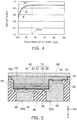
- FIG. 4 is a graph illustrating the configuration of a part of the semiconductor light emitting device according to the embodiment.
- the drawing shows the relationship between the thickness of the Al film included in the seed layer 47 and the reflectance of the Al film, for example.
- Graph D is the reflectance when light is perpendicularly incident on the Al film
- graph E is the reflectance when integrating over solid angle. As shown in the drawing, a reflectance of 89% or more is obtained when the thickness of the Al film is 30 nm or more.
- the seed layer 47 preferably uses, for its surface in contact with the insulating layer 70, aluminum or an alloy thereof with a reflectance at light wavelengths ranging from 400 nm to 750 nm of 80% or more, or silver or an alloy thereof with a higher reflectance than aluminum.
- the seed layer 47 preferably includes, for example, an Al film with a thickness of 30 nm or more.
- the thickness of the first conversion electrode 43 and the second conversion electrode 53 is set, for example, not less than 1 ⁇ m and not more than 100 ⁇ m.
- the thickness of each conversion electrode may be appropriately set in view of heat dissipation performance, electrical characteristics, and productivity.
- the insulating layer 70 may include at least one of silicon oxide and silicon nitride.
- an inorganic material such as SiO 2 , SiN, phosphorus silicate glass (PSG), and boron phosphorus silicate glass (BPSG) may be used.
- the insulating layer 70 is formed by CVD, for example.
- the thickness of the insulating layer 70 is, for example, not less than 10 nm and not more than 10,000 nm and is preferably 400 nm.
- CVD chemical vapor deposition, sputtering, or the like may be used as well as CVD.
- a glass material such as organic SOG (spin on glass) and inorganic SOG may be used as the insulating layer 70.
- a methylsilsesquioxane film may be used as the organic SOG film, for example.
- a silsesquioxane hydride film may be used as the inorganic SOG film.
- a film formed by applying an alcohol solution of a silanol and performing heat treatment may be used as the inorganic SOG film, for example.
- a low dielectric constant interlayer insulating film (low-k film) and the like may be used as the insulating layer 70.
- a resin-based material such as a polyimide, polybenzoxazole (PBO), and a silicone-based material may be used as the insulating layer 70.
- the thickness of the insulating layer 70 is, for example, not less than 1000 nm and not more than 20,000 nm.
- the reflectance of the insulating layer 70 is lower than the reflectance of the first conversion electrode 43 and the second conversion electrode 53, when a light transmissive material is used for the insulating layer 70, for example.
- the p-side conductive layer 42 serves as a contact electrode to the second semiconductor layer 20.
- a film containing at least one of Ni, Au, Ag, Al, and Pd may be used, for example.
- a stacked film including at least two selected from a Ni film, a Au film, a Ag film, an Al film, and a Pd film may be used.
- Preferably one of a Ag film, an Al film, and a Pd film, or a stacked film including at least two of a Ag film, an Al film, and a Pd film is used as the p-side conductive layer 42.
- a light transmissive metal oxide may be used as the p-side conductive layer 42.
- ITO indium tin oxide
- SnO 2 indium tin oxide
- In 2 O 3 in 2 O 3
- ZnO ZnO
- Sputtering, vapor deposition, and the like may be used for the formation of the p-side conductive layer 42, for example.
- the thickness of the p-side conductive layer 42 is, for example, 0.2 ⁇ m.
- a stacked film of a Ni film and a Au film may be used, for example.
- the thickness of the Ni film is about 100 nm, for example, and the thickness of the Au film is, for example, about 100 nm.
- a stacked film of a Ti film, a Ni film, and a Au film may be used as the p-side electrode 41 and the second electrode 50, for example.
- the thickness of the Ti film is, for example, 50 nm; the thickness of the Ni film is, for example, about 100 nm; and the thickness of the Au film is, for example, about 100 nm.
- the material, the thickness, and the configuration of the p-side electrode 41 are preferably the same as the material, the thickness, and the configuration of the second electrode 50. Sputtering and vapor deposition may be used for forming the p-side electrode 41 and the second electrode 50, for example.
- an insulating resin such as an epoxy resin may be used, for example.
- the sealing body 80 may include, for example, a quartz filler, an alumina filler, or the like. By including these fillers, the sealing body 80 has improved thermal conductivity and enables heat dissipation performance to be improved.
- the sealing body 80 may include, for example, a filler containing at least one selected from the group consisting of ZnO, TiO 2 , ZrO 2 , Al 2 O 3 , MgO, CaTiO 2 , BaSO 4 , ZnS, and CaCO 3 .
- a filler containing at least one selected from the group consisting of ZnO, TiO 2 , ZrO 2 , Al 2 O 3 , MgO, CaTiO 2 , BaSO 4 , ZnS, and CaCO 3 .
- the filler that improves thermal conductivity and the filler that improves the reflectance mentioned above may be mixed for use.
- the embodiment is not limited thereto, and any insulating material may be used for the sealing body 80.
- a filler may not be included.
- FIG. 5 is a schematic cross-sectional view illustrating the configuration of a semiconductor light emitting device 110 according to a variation of the embodiment.
- the semiconductor light emitting device 110 according to the embodiment further includes a wavelength conversion layer 90.
- Other components and the combination thereof are the same as those of the semiconductor light emitting device 100.
- the wavelength conversion layer 90 is provided on at least a part of the first surface 15f of the stacked body 15.
- the wavelength conversion layer 90 absorbs a part of the light emission in the light emitting layer 30, and emits light with a wavelength different therefrom.
- the wavelength conversion layer 90 includes, for example, a fluorescent substance.
- the fluorescent substance included in the wavelength conversion layer 90 may include a plurality of fluorescent substances that emit lights of wavelengths different from one another.
- the wavelength conversion layer 90 may be a structure in which a plurality of fluorescent layers individually including different types of fluorescent substances are stacked.
- the light emitted from the light emitting layer 30 is ultraviolet light, violet light, or blue light
- the light emitted from the fluorescent substance is yellow light or red light.
- the mixed lights emitted from the wavelength conversion layer 90 (converted light) and the light emitting layer 30 make white light, for example.
- the wavelength conversion layer 90 covers the entire first surface 15f.
- the embodiment is not limited thereto, and a part of the first surface 15f may not be covered with the wavelength conversion layer 90.
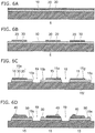
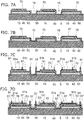
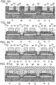
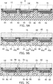
- FIG. 6A to FIG. 9C are schematic cross-sectional views showing an example of the manufacturing process of the semiconductor light emitting device 110.
- a plurality of semiconductor light emitting devices 110 are collectively formed in one wafer.
- FIG. 6A is a cross-sectional view showing the first semiconductor layer 10, the second semiconductor layer 20, and the light emitting layer 30 formed on a substrate 5.
- the first semiconductor layer 10, the light emitting layer 30, and the second semiconductor layer 20 are caused to grow sequentially on the substrate 5 using the MOCVD (metal organic chemical vapor deposition) method, for example.
- the substrate 5 is a silicon substrate, for example. Also a sapphire substrate may be used as the substrate 5.
- the first semiconductor layer 10, the light emitting layer 30, and the second semiconductor layer 20 are, for example, a nitride semiconductor and contain gallium nitride (GaN).
- the first semiconductor layer 10 is an n-type GaN layer, for example.
- the first semiconductor layer 10 may have a stacked structure including a buffer layer provided on the substrate 5 and an n-type GaN layer provided on the buffer layer.
- the second semiconductor layer 20 includes, for example, a p-type AIGaN layer provided on the light emitting layer 30 and a p-type GaN layer provided on the p-type AIGaN layer, for example.
- FIG. 6B shows a state where the second semiconductor layer 20 and the light emitting layer 30 are selectively removed to expose the first semiconductor layer 10.
- a not-shown etching mask is used to selectively etch the second semiconductor layer 20 and the light emitting layer 30 to expose the first semiconductor layer 10.
- the RIE (reactive ion etching) method is used for the etching of the second semiconductor layer 20 and the light emitting layer 30, for example.
- the first semiconductor layer 10 is selectively removed to form a plurality of stacked bodies 15 on the substrate 5.
- an etching mask (not shown) that covers the second semiconductor layer 20 and the light emitting layer 30 is provided on the first semiconductor layer 10.
- the RIE method is used to etch the first semiconductor layer 10 to form trenches 19 with a depth reaching the substrate 5.
- the trench 19 is formed deeper than the first surface 15f by etching the substrate 5. It is also possible to form the trench 19 after forming the first electrode 40 and the second electrode 50.
- the outer edge side surface 15s of the stacked body 15, which is the sidewall of the trench 19, is made a tapered shape inclined such that the stacked body 15 on the second surface 15g side is narrower, for example.
- the area of the stacked body 15 on the second surface 15g side is preferably smaller that on the first surface 15f.
- the first surface 15f of the stacked body 15 is the surface in contact with the substrate 5
- the second surface 15g is the surfaces of the first semiconductor layer 10 and the second semiconductor layer 20.
- the first electrode 40 and the second electrode 50 are formed on the second surface 15g of the stacked body 15.
- the first electrode 40 is formed on the second semiconductor layer 20.
- the second electrode 50 is formed on the first semiconductor layer 10.
- the first electrode 40 is formed so as to have a larger area than the second electrode 50.
- the first electrode 40 and the second electrode 50 are formed by the sputtering method, the vapor deposition method, or the like, for example. Either of the first electrode 40 and the second electrode 50 may be formed earlier, or both may be formed simultaneously using the same material.
- the insulating layer 70 that covers the stacked body 15 is formed on the substrate 5.
- An opening leading to the first electrode 40 provided on the stacked body 15 and an opening leading to the second electrode 50 are formed in the insulating layer 70.
- a metal film (the seed layer 47) is formed on the insulating layer 70.
- the seed layer 47 covers the first electrode 40 and the second electrode 50 exposed at the openings of the insulating layer 70.
- the seed layer 47 preferably includes, at the surface in contact with the insulating layer 70, for example, a member with a reflectance of 80% or more for the light emission of the light emitting layer 30.
- a resist mask 91 is formed on the seed layer 47.
- the resist mask 91 includes openings 91a and openings 91b.
- the opening 91a is provided on the first electrode 40, and the opening 91b is provided on the second electrode 50.
- electroplating is used to form the first conversion electrode 43, the second conversion electrode 53, and the light blocking body 57 covering the inner surface of the trench 19. That is, the seed layer 47 is used as a current path to perform plating to form copper (Cu), for example, in the openings 91a and 91b of the resist mask 91 and in the trench 19; thus, the first conversion electrode 43, the second conversion electrode 53, and the light blocking body 57 are selectively formed.
- Cu copper
- the first conversion electrode 43 is electrically connected to the first electrode 40 via the opening of the insulating layer 70.
- the second conversion electrode 53 is electrically connected to the second electrode 50 via the opening of the insulating layer 70.
- a resist mask 92 having openings 92a and openings 92b is formed.
- a resist mask 91 is newly formed using photolithography. It is also possible to form the resist mask 92 on the resist mask 91 in a stacked manner.
- the first pillar 45 and the second pillar 55 are formed in the openings 92a and 92b, respectively.
- the first pillar 45 and the second pillar 55 are formed, for example, using electroplating.
- the first pillar 45 and the second pillar 55 are formed, for example, by copper plating.
- the resist mask 92 is removed, for example, using a solvent or oxygen plasma.
- the first pillar 45, the second pillar 55, the first conversion electrode 43, and the second conversion electrode 53 are used as a mask to perform wet etching to remove the exposed portion of the seed layer 47. Thereby, the electrical connection between the first conversion electrode 43 and the second conversion electrode 53 is cut.
- the sealing body 80 that covers the upper side of the insulating layer 70, the first pillar 45, and the second pillar 55 is formed.
- the sealing body 80 contains, for example, carbon black, and blocks the light emitted from the light emitting layer 30.
- the sealing body 80 may include a member that reflects the light emitted from the light emitting layer 30, for example, such as titanium oxide.
- FIGS. 9A to 9C are cross-sectional views illustrating the stacked body 15 and the sealing body 80 so as to be upside down view of FIG. 8D .
- the substrate 5 When using a silicon substrate, selectively removing the substrate 5 by using wet etching becomes possible, for example.
- the substrate 5 When the substrate 5 is a sapphire substrate, the substrate 5 may be removed, for example, by using the laser lift-off method.
- the first semiconductor layer 10 is wet-etched, for example, using a KOH (potassium hydroxide) aqueous solution, TMAH (tetramethylammonium hydroxide), or the like.
- KOH potassium hydroxide
- TMAH tetramethylammonium hydroxide
- a difference in etching rate depending on the crystal plane orientation makes the fine protrusions in the first surface 15f as shown in FIG. 9A .
- the fine protrusions provided in the first surface 15f may improve the extraction efficiency of the light emitted from the light emitting layer 30.
- the wavelength conversion layer 90 is formed on the first surface 15f.
- the wavelength conversion layer 90 is a resin layer in which a fluorescent substance 95 is dispersed, for example.
- the wavelength conversion layer 90 is formed, for example, using a method such as printing, potting, molding, and compression molding.
- the surface of the sealing body 80 is ground to expose the ends of the first pillar 45 and the second pillar 55.
- the end 45e of the first pillar 45 functions as a p-side external terminal, for example, and the end 55e of the second pillar 55 functions as an n-side external terminal, for example.
- the wavelength conversion layer 90, the insulating layer 70, and the sealing body 80 are cut between adjacent stacked bodies 15. Thereby, the semiconductor light emitting device 100 including the stacked body 15 is fragmented.
- the cutting of the wavelength conversion layer 90, the insulating layer 70, and the sealing body 80 is performed using a dicing blade, for example. Laser irradiation may also be used for the cutting.
- FIG. 10A and FIG. 10B are schematic views illustrating the configuration of the semiconductor light emitting device 120 according to the embodiment.
- the semiconductor light emitting device 120 in a state where the first pillar 45, the second pillar 55, and the sealing body 80 are removed is illustrated in order to describe the configuration of the first conversion electrode 43, the second conversion electrode 53, and the light blocking body 57.
- FIG. 10A is a plan view
- FIG. 10B is a cross-sectional view taken along line C-C of FIG. 10A .
- the second electrode 50 is provided at the center of the stacked body 15. That is, the second portion 15b is provided in a central portion in the X-direction of the stacked body 15, and the first portion 15a is provided on both sides of the second portion 15b.
- the insulating layer 70 covers the outer edge side surface 15s and a part of the second surface 15g of the stacked body 15.
- the insulating layer 70 further covers at least a part of the boundary side surface 15t between the first portion 15a and the second portion 15b. In this example, the insulating layer 70 covers the entire boundary side surface 15t.
- the first conversion electrode 43 and the second conversion electrode 53 are provided on the second surface 15g side of the stacked body 15.
- the first conversion electrode 43 is formed so as to cover the first electrodes 40 on the second surface side of the two first portions 15a.
- the second conversion electrode 53 is provided on the second surface side of the second portion 15b, and extends across the boundary side surface 15t to the first portion 15a side.
- the light blocking body 57 covers at least a part of the outer edge side surface 15s of the stacked body 15.
- the second conversion electrode 53 covers at least a part of the boundary side surface 15t between the first electrode 40 and the second electrode 50.
- the second conversion electrode 53 is provided so as to cover the spaces between the two first electrodes 40 and the second electrode 50 provided between them.
- the second conversion electrode 53 reflects light leaking from between the first electrode 40 and the second electrode 50.
- the light blocking body 57 is formed so as to cover at least a part of the outer edge side surface 15s. Thereby, light leaking from the outer edge side surface 15s and the boundary side surface 15t can be reflected and extracted. Thereby, the light emission efficiency of the semiconductor light emitting device 120 can be improved.
- the "nitride semiconductor” referred to herein includes group III-V compound semiconductors of B x In y Al z Ga 1-x-y-z N (0 ⁇ x ⁇ 1, 0 ⁇ y ⁇ 1, 0 ⁇ z ⁇ 1, 0 ⁇ x+y+z ⁇ 1), and also includes mixed crystals containing a group V element besides N (nitrogen), such as phosphorus (P) and arsenic (As). Furthermore, the “nitride semiconductor” also includes those further containing various elements added to control various material properties such as conductivity type, and those further containing various unintended elements.
Landscapes
- Led Devices (AREA)
- Led Device Packages (AREA)
Claims (17)
- Lichtemittierende Halbleiterdiodenvorrichtung (100, 110, 120), wobei die Vorrichtung umfasst:einen Stapelkörper (15), der eine erste Halbleiterschicht (10) eines ersten Leitfähigkeitstyps, eine zweite Halbleiterschicht (20) eines zweiten Leitfähigkeitstyps und eine lichtemittierende Schicht (30) enthält, die zwischen der ersten Halbleiterschicht und der zweiten Halbleiterschicht bereitgestellt ist,wobei ein erster Abschnitt (15a) des Stapelkörpers (15) enthält:einen Teil der ersten Halbleiterschicht (10), wobei die lichtemittierende Schicht (30) auf dem Teil der ersten Halbleiterschicht (10) bereitgestellt ist, unddie zweite Halbleiterschicht (20), die auf der lichtemittierenden Schicht (30) bereitgestellt ist, undwobei ein zweiter Abschnitt (15b) des Stapelkörpers (15) neben dem ersten Abschnitt (15a) bereitgestellt ist und einen weiteren Teil der ersten Halbleiterschicht (10) enthält;eine erste Elektrode (40), die auf der zweiten Halbleiterschicht (20) auf einer Seite des Stapelkörpers (15) bereitgestellt ist;eine zweite Elektrode (50), die auf dem anderen Teil der ersten Halbleiterschicht (10) auf der Seite des Stapelkörpers (15) bereitgestellt ist;eine Isolierschicht (70), die den Stapelkörper (15) auf der Seite des Stapelkörpers (15) bedeckt, auf der die erste Elektrode (40) und die zweite Elektrode (50) bereitgestellt sind, wobei die Isolierschicht (70) weiter eine Seitenfläche um den Stapelkörper (15) herum bedeckt;eine erste Umwandlungselektrode (43), die auf der Isolierschicht (70) bereitgestellt ist und elektrisch mit der ersten Elektrode (40) verbunden ist;eine zweite Umwandlungselektrode (53), die neben der ersten Umwandlungselektrode (43) auf der Isolierschicht (70) bereitgestellt ist und elektrisch mit der zweiten Elektrode (50) verbunden ist;eine erste Säule (45), die an der ersten Umwandlungselektrode (43) bereitgestellt ist und sich in einer ersten Richtung von der ersten Halbleiterschicht (10) zu der zweiten Halbleiterschicht (20) erstreckt;eine zweite Säule (55), die an der zweiten Umwandlungselektrode (53) bereitgestellt ist und sich in der ersten Richtung erstreckt;einen Dichtungskörper (80), der den Stapelkörper (15), die erste Säule (45) und die zweite Säule (55) bedeckt, wobei ein Ende der ersten Säule (45) und ein Ende der zweiten Säule (55) in dem Dichtungskörper (80) freigelegt sind;einen Lichtblockierkörper (57), der auf der Seitenfläche des Stapelkörpers (15) über die Isolierschicht (70) bereitgestellt wird, wobei der Lichtblockierkörper (57) eine Seitenfläche der ersten Halbleiterschicht (10) bedeckt und die erste Umwandlungselektrode (43) und die zweite Umwandlungselektrode (53) umgibt, undeine Wellenlängen-Umwandlungsschicht (90) auf einer Seite des Stapelkörpers (15) gegenüber der Seite bereitgestellt sind, auf der die erste Elektrode (40) und die zweite Elektrode (50) bereitgestellt sind, wobei die erste Halbleiterschicht (10) zwischen der lichtemittierenden Schicht (30) und der Wellenlängen-Umwandlungsschicht (90) positioniert ist, wobei sich die Wellenlängen-Umwandlungsschicht über den Lichtblockierkörper (57) erstreckt, und kein Substrat zwischen dem Stapelkörper (15) und der Wellenlängen-Umwandlungsschicht (90) und zwischen dem Lichtblockierkörper (57) und der Wellenlängen-Umwandlungsschicht (90) bereitgestellt ist,wobei die erste Umwandlungselektrode (43), die zweite Umwandlungselektrode (53) und der Lichtblockierkörper (57) jeweils eine erste Metallschicht (47) und eine zweite Metallschicht (49) enthalten, die auf der ersten Metallschicht (47) bereitgestellt ist, wobei die erste Metallschicht (47) in Kontakt mit der Isolierschicht (70) ist und Aluminium enthält.
- Vorrichtung nach Anspruch 1, wobei sich die zweite Umwandlungselektrode (53) auf der Isolierschicht (70) von dem zweiten Abschnitt (15b) zu dem ersten Abschnitt (15a) erstreckt; und
die zweite Umwandlungselektrode (53) eine Seitenfläche der lichtemittierenden Schicht (30) und eine Seitenfläche der zweiten Halbleiterschicht (20) bedeckt, die sich zwischen dem ersten Abschnitt (15a) und dem zweiten Abschnitt (15b) befindet. - Vorrichtung nach Anspruch 1 oder 2, wobei die erste Metallschicht (47) eine Dicke von 30 nm oder mehr aufweist.
- Vorrichtung nach einem der Ansprüche 1 bis 3, wobei der Lichtblockierkörper (57) elektrisch mit einer der ersten Umwandlungselektrode (43) und der zweiten Umwandlungselektrode (53) verbunden ist.
- Vorrichtung nach einem der Ansprüche 1 bis 3, wobei der Lichtblockierkörper (57) elektrisch von der ersten Umwandlungselektrode (43) und der zweiten Umwandlungselektrode (53) isoliert ist.
- Vorrichtung nach einem der Ansprüche 1 bis 5, wobei die Seitenfläche des Stapelkörpers (15) geneigt ist, so dass die erste Halbleiterschicht (10) auf der Seite der lichtemittierenden Schicht (30) eine kleinere Fläche als auf einer gegenüberliegenden Seite davon aufweist.
- Vorrichtung nach einem der Ansprüche 1 bis 6, wobei die erste Elektrode (40) mindestens eines von Ni, Au, Ag, AI und Pd enthält.
- Vorrichtung nach einem der Ansprüche 1 bis 6, wobei die erste Elektrode (40) eine Stapelstruktur aufweist, die mindestens zwei von einem Ag-Film, einem Al-Film und einem Pd-Film enthält.
- Vorrichtung nach einem der Ansprüche 1 bis 6, wobei die erste Elektrode ein Metalloxid enthält, das von der lichtemittierenden Schicht emittiertes Licht überträgt.
- Vorrichtung nach Anspruch 9, wobei die erste Elektrode (40) eines von ITO (Indiumzinnoxid), SnO2, In2O3 und ZnO enthält.
- Vorrichtung nach einem der Ansprüche 1 bis 10, wobei die lichtemittierende Schicht (30) Licht emittiert, das eine Spitzenwellenlänge von nicht weniger als 350 Nanometer und nicht mehr als 700 Nanometer aufweist.
- Vorrichtung nach einem der Ansprüche 1 bis 11, wobei die erste Umwandlungselektrode (43) und die zweite Umwandlungselektrode (53) eine Dicke von nicht weniger als 1 Mikrometer und nicht mehr als 100 Mikrometer aufweisen.
- Vorrichtung nach einem der Ansprüche 1 bis 12, wobei die Isolierschicht (70) ein anorganisches Material enthält.
- Vorrichtung nach Anspruch 13, wobei die Isolierschicht (70) mindestens eines von Siliciumoxid und Siliciumnitrid enthält.
- Vorrichtung nach einem der Ansprüche 1 bis 14, wobei die zweite Umwandlungselektrode (53) einen Raum zwischen der ersten Elektrode (40) und der zweiten Elektrode (50) über die Isolierschicht bedeckt.
- Vorrichtung nach einem der Ansprüche 1 bis 15,
wobei die erste Umwandlungselektrode (43) einen Abschnitt aufweist, der zwischen der ersten Elektrode (40) und der ersten Säule (45) bereitgestellt ist, und
die zweite Umwandlungselektrode (53) einen Abschnitt aufweist, der zwischen der zweiten Elektrode (50) und der zweiten Säule (55) bereitgestellt ist. - Vorrichtung nach Anspruch 16, wobei
der Dichtungskörper (80) einen Füllstoff enthält und
der Füllstoff mindestens eines enthält, das aus der Gruppe, bestehend aus ZnO, TiO2, ZrO2, Al2O3, MgO, CaTiO2, BaSO4, ZnS und CaCO3 ausgewählt ist.
Applications Claiming Priority (1)
| Application Number | Priority Date | Filing Date | Title |
|---|---|---|---|
| JP2013194108A JP6306308B2 (ja) | 2013-09-19 | 2013-09-19 | 半導体発光装置 |
Publications (2)
| Publication Number | Publication Date |
|---|---|
| EP2851970A1 EP2851970A1 (de) | 2015-03-25 |
| EP2851970B1 true EP2851970B1 (de) | 2018-03-14 |
Family
ID=51265616
Family Applications (1)
| Application Number | Title | Priority Date | Filing Date |
|---|---|---|---|
| EP14180009.4A Active EP2851970B1 (de) | 2013-09-19 | 2014-08-06 | Leuchtdioden-Halbleiterbauelement |
Country Status (6)
| Country | Link |
|---|---|
| US (1) | US9142727B2 (de) |
| EP (1) | EP2851970B1 (de) |
| JP (1) | JP6306308B2 (de) |
| KR (1) | KR20150032621A (de) |
| CN (1) | CN104465970A (de) |
| TW (1) | TWI560902B (de) |
Families Citing this family (11)
| Publication number | Priority date | Publication date | Assignee | Title |
|---|---|---|---|---|
| JP6295171B2 (ja) | 2014-09-16 | 2018-03-14 | アルパッド株式会社 | 発光ユニット及び半導体発光装置 |
| JP6555907B2 (ja) | 2015-03-16 | 2019-08-07 | アルパッド株式会社 | 半導体発光装置 |
| DE102015114587A1 (de) * | 2015-09-01 | 2017-03-02 | Osram Opto Semiconductors Gmbh | Optoelektronisches Halbleiterbauelement und Verfahren zu dessen Herstellung |
| JP2017168808A (ja) * | 2015-11-06 | 2017-09-21 | 株式会社カネカ | Csp−led用熱硬化性白色インク |
| KR102417181B1 (ko) | 2015-11-09 | 2022-07-05 | 삼성전자주식회사 | 발광 패키지, 반도체 발광 소자, 발광 모듈 및 발광 패키지의 제조 방법 |
| TWI557701B (zh) * | 2015-12-30 | 2016-11-11 | 友達光電股份有限公司 | 應用於製作發光元件陣列顯示器的印刷板模及發光元件陣列顯示器 |
| DE102016103059A1 (de) * | 2016-02-22 | 2017-08-24 | Osram Opto Semiconductors Gmbh | Halbleiterbauelement und Verfahren zur Herstellung eines Halbleiterbauelements |
| US10043956B2 (en) | 2016-09-29 | 2018-08-07 | Nichia Corporation | Method for manufacturing light emitting device |
| CN109712967B (zh) | 2017-10-25 | 2020-09-29 | 隆达电子股份有限公司 | 一种发光二极管装置及其制造方法 |
| JP7216296B2 (ja) | 2020-09-30 | 2023-02-01 | 日亜化学工業株式会社 | 発光素子及び発光装置 |
| KR102752045B1 (ko) | 2021-10-05 | 2025-01-09 | 삼성전자주식회사 | 반도체 발광 소자, 이를 포함하는 디스플레이 장치, 및 반도체 발광 소자를 제조하는 방법 |
Citations (3)
| Publication number | Priority date | Publication date | Assignee | Title |
|---|---|---|---|---|
| JP2001044498A (ja) * | 1999-07-28 | 2001-02-16 | Nichia Chem Ind Ltd | 窒化物半導体発光素子 |
| EP2302708A2 (de) * | 2009-09-25 | 2011-03-30 | Kabushiki Kaisha Toshiba | Lichtemittierendes Halbleiterbauelement und Herstellungsverfahren |
| EP2546894A2 (de) * | 2011-07-12 | 2013-01-16 | Kabushiki Kaisha Toshiba | Lichtemittierendes Halbleiterbauelement |
Family Cites Families (11)
| Publication number | Priority date | Publication date | Assignee | Title |
|---|---|---|---|---|
| JP3531475B2 (ja) * | 1998-05-22 | 2004-05-31 | 日亜化学工業株式会社 | フリップチップ型光半導体素子 |
| JP4678211B2 (ja) | 2005-02-28 | 2011-04-27 | 三菱化学株式会社 | 発光装置 |
| JP2008205005A (ja) | 2007-02-16 | 2008-09-04 | Mitsubishi Chemicals Corp | GaN系LED素子 |
| US20090173956A1 (en) | 2007-12-14 | 2009-07-09 | Philips Lumileds Lighting Company, Llc | Contact for a semiconductor light emitting device |
| JP2009260316A (ja) * | 2008-03-26 | 2009-11-05 | Panasonic Electric Works Co Ltd | 半導体発光素子およびそれを用いる照明装置 |
| JP5337106B2 (ja) * | 2010-06-04 | 2013-11-06 | 株式会社東芝 | 半導体発光装置 |
| JP5414627B2 (ja) * | 2010-06-07 | 2014-02-12 | 株式会社東芝 | 半導体発光装置及びその製造方法 |
| KR101230622B1 (ko) * | 2010-12-10 | 2013-02-06 | 이정훈 | 집단 본딩을 이용한 반도체 디바이스 제조 방법 및 그것에 의해 제조된 반도체 디바이스 |
| JP5304855B2 (ja) | 2011-08-12 | 2013-10-02 | 三菱化学株式会社 | GaN系発光ダイオードおよびそれを用いた発光装置 |
| JP5949294B2 (ja) | 2011-08-31 | 2016-07-06 | 日亜化学工業株式会社 | 半導体発光素子 |
| JP2013084889A (ja) | 2011-09-30 | 2013-05-09 | Toshiba Corp | 半導体発光装置及びその製造方法 |
-
2013
- 2013-09-19 JP JP2013194108A patent/JP6306308B2/ja active Active
-
2014
- 2014-07-29 US US14/445,261 patent/US9142727B2/en active Active
- 2014-08-01 KR KR20140099037A patent/KR20150032621A/ko not_active Ceased
- 2014-08-06 EP EP14180009.4A patent/EP2851970B1/de active Active
- 2014-08-18 TW TW103128342A patent/TWI560902B/zh active
- 2014-08-19 CN CN201410407696.XA patent/CN104465970A/zh active Pending
Patent Citations (3)
| Publication number | Priority date | Publication date | Assignee | Title |
|---|---|---|---|---|
| JP2001044498A (ja) * | 1999-07-28 | 2001-02-16 | Nichia Chem Ind Ltd | 窒化物半導体発光素子 |
| EP2302708A2 (de) * | 2009-09-25 | 2011-03-30 | Kabushiki Kaisha Toshiba | Lichtemittierendes Halbleiterbauelement und Herstellungsverfahren |
| EP2546894A2 (de) * | 2011-07-12 | 2013-01-16 | Kabushiki Kaisha Toshiba | Lichtemittierendes Halbleiterbauelement |
Also Published As
| Publication number | Publication date |
|---|---|
| JP6306308B2 (ja) | 2018-04-04 |
| EP2851970A1 (de) | 2015-03-25 |
| US9142727B2 (en) | 2015-09-22 |
| TW201519466A (zh) | 2015-05-16 |
| US20150076546A1 (en) | 2015-03-19 |
| JP2015060964A (ja) | 2015-03-30 |
| CN104465970A (zh) | 2015-03-25 |
| TWI560902B (en) | 2016-12-01 |
| KR20150032621A (ko) | 2015-03-27 |
Similar Documents
| Publication | Publication Date | Title |
|---|---|---|
| EP2851970B1 (de) | Leuchtdioden-Halbleiterbauelement | |
| CN103403888B (zh) | 半导体发光器件及其制造方法 | |
| US9444013B2 (en) | Semiconductor light emitting device and method for manufacturing the same | |
| TWI429108B (zh) | 半導體發光裝置 | |
| US9136439B2 (en) | Semiconductor light emitting device | |
| WO2014192237A1 (ja) | 半導体発光素子及び半導体発光装置 | |
| US9293657B2 (en) | Semiconductor light emitting device | |
| CN103415937A (zh) | 发光器件、发光模块以及用于制造发光器件的方法 | |
| US9698305B2 (en) | High voltage LED flip chip | |
| US20150263241A1 (en) | Semiconductor light emitting device | |
| CN103168369B (zh) | 光电子器件和用于该光电子器件制造的方法 | |
| US11239392B2 (en) | Optoelectronic semiconductor chip, high-voltage semiconductor chip and method for producing an optoelectronic semiconductor chip | |
| KR20130066308A (ko) | 발광소자 | |
| US20230238485A1 (en) | Light emitting device and method of manufacturing the same | |
| KR101055778B1 (ko) | 발광 다이오드 및 이의 제조 방법 | |
| US20240413265A1 (en) | Method for manufacturing light-emitting device | |
| KR102217128B1 (ko) | 발광 다이오드 및 그 제조 방법 | |
| HK1188333B (en) | Semiconductor light-emitting device | |
| HK1190828A (en) | Semiconductor light emitting device |
Legal Events
| Date | Code | Title | Description |
|---|---|---|---|
| PUAI | Public reference made under article 153(3) epc to a published international application that has entered the european phase |
Free format text: ORIGINAL CODE: 0009012 |
|
| 17P | Request for examination filed |
Effective date: 20140806 |
|
| AK | Designated contracting states |
Kind code of ref document: A1 Designated state(s): AL AT BE BG CH CY CZ DE DK EE ES FI FR GB GR HR HU IE IS IT LI LT LU LV MC MK MT NL NO PL PT RO RS SE SI SK SM TR |
|
| AX | Request for extension of the european patent |
Extension state: BA ME |
|
| STAA | Information on the status of an ep patent application or granted ep patent |
Free format text: STATUS: EXAMINATION IS IN PROGRESS |
|
| 17Q | First examination report despatched |
Effective date: 20170209 |
|
| GRAP | Despatch of communication of intention to grant a patent |
Free format text: ORIGINAL CODE: EPIDOSNIGR1 |
|
| STAA | Information on the status of an ep patent application or granted ep patent |
Free format text: STATUS: GRANT OF PATENT IS INTENDED |
|
| INTG | Intention to grant announced |
Effective date: 20171219 |
|
| GRAS | Grant fee paid |
Free format text: ORIGINAL CODE: EPIDOSNIGR3 |
|
| GRAA | (expected) grant |
Free format text: ORIGINAL CODE: 0009210 |
|
| STAA | Information on the status of an ep patent application or granted ep patent |
Free format text: STATUS: THE PATENT HAS BEEN GRANTED |
|
| AK | Designated contracting states |
Kind code of ref document: B1 Designated state(s): AL AT BE BG CH CY CZ DE DK EE ES FI FR GB GR HR HU IE IS IT LI LT LU LV MC MK MT NL NO PL PT RO RS SE SI SK SM TR |
|
| REG | Reference to a national code |
Ref country code: GB Ref legal event code: FG4D |
|
| REG | Reference to a national code |
Ref country code: AT Ref legal event code: REF Ref document number: 979644 Country of ref document: AT Kind code of ref document: T Effective date: 20180315 Ref country code: CH Ref legal event code: EP |
|
| REG | Reference to a national code |
Ref country code: IE Ref legal event code: FG4D |
|
| REG | Reference to a national code |
Ref country code: DE Ref legal event code: R096 Ref document number: 602014022260 Country of ref document: DE |
|
| REG | Reference to a national code |
Ref country code: NL Ref legal event code: FP |
|
| REG | Reference to a national code |
Ref country code: DE Ref legal event code: R082 Ref document number: 602014022260 Country of ref document: DE Representative=s name: KUHNEN & WACKER PATENT- UND RECHTSANWALTSBUERO, DE Ref country code: DE Ref legal event code: R082 Ref document number: 602014022260 Country of ref document: DE Representative=s name: HOFFMANN - EITLE PATENT- UND RECHTSANWAELTE PA, DE Ref country code: DE Ref legal event code: R081 Ref document number: 602014022260 Country of ref document: DE Owner name: SAMSUNG ELECTRONICS CO., LTD., SUWON-SI, KR Free format text: FORMER OWNER: KABUSHIKI KAISHA TOSHIBA, TOKYO, JP Ref country code: DE Ref legal event code: R081 Ref document number: 602014022260 Country of ref document: DE Owner name: TOSHIBA ELECTRONIC DEVICES & STORAGE CORPORATI, JP Free format text: FORMER OWNER: KABUSHIKI KAISHA TOSHIBA, TOKYO, JP |
|
| REG | Reference to a national code |
Ref country code: FR Ref legal event code: PLFP Year of fee payment: 5 |
|
| REG | Reference to a national code |
Ref country code: LT Ref legal event code: MG4D |
|
| PG25 | Lapsed in a contracting state [announced via postgrant information from national office to epo] |
Ref country code: FI Free format text: LAPSE BECAUSE OF FAILURE TO SUBMIT A TRANSLATION OF THE DESCRIPTION OR TO PAY THE FEE WITHIN THE PRESCRIBED TIME-LIMIT Effective date: 20180314 Ref country code: HR Free format text: LAPSE BECAUSE OF FAILURE TO SUBMIT A TRANSLATION OF THE DESCRIPTION OR TO PAY THE FEE WITHIN THE PRESCRIBED TIME-LIMIT Effective date: 20180314 Ref country code: NO Free format text: LAPSE BECAUSE OF FAILURE TO SUBMIT A TRANSLATION OF THE DESCRIPTION OR TO PAY THE FEE WITHIN THE PRESCRIBED TIME-LIMIT Effective date: 20180614 Ref country code: CY Free format text: LAPSE BECAUSE OF FAILURE TO SUBMIT A TRANSLATION OF THE DESCRIPTION OR TO PAY THE FEE WITHIN THE PRESCRIBED TIME-LIMIT Effective date: 20180314 Ref country code: LT Free format text: LAPSE BECAUSE OF FAILURE TO SUBMIT A TRANSLATION OF THE DESCRIPTION OR TO PAY THE FEE WITHIN THE PRESCRIBED TIME-LIMIT Effective date: 20180314 |
|
| RAP2 | Party data changed (patent owner data changed or rights of a patent transferred) |
Owner name: TOSHIBA ELECTRONIC DEVICES & STORAGE CORPORATION |
|
| REG | Reference to a national code |
Ref country code: AT Ref legal event code: MK05 Ref document number: 979644 Country of ref document: AT Kind code of ref document: T Effective date: 20180314 |
|
| PG25 | Lapsed in a contracting state [announced via postgrant information from national office to epo] |
Ref country code: SE Free format text: LAPSE BECAUSE OF FAILURE TO SUBMIT A TRANSLATION OF THE DESCRIPTION OR TO PAY THE FEE WITHIN THE PRESCRIBED TIME-LIMIT Effective date: 20180314 Ref country code: LV Free format text: LAPSE BECAUSE OF FAILURE TO SUBMIT A TRANSLATION OF THE DESCRIPTION OR TO PAY THE FEE WITHIN THE PRESCRIBED TIME-LIMIT Effective date: 20180314 Ref country code: BG Free format text: LAPSE BECAUSE OF FAILURE TO SUBMIT A TRANSLATION OF THE DESCRIPTION OR TO PAY THE FEE WITHIN THE PRESCRIBED TIME-LIMIT Effective date: 20180614 Ref country code: GR Free format text: LAPSE BECAUSE OF FAILURE TO SUBMIT A TRANSLATION OF THE DESCRIPTION OR TO PAY THE FEE WITHIN THE PRESCRIBED TIME-LIMIT Effective date: 20180615 Ref country code: RS Free format text: LAPSE BECAUSE OF FAILURE TO SUBMIT A TRANSLATION OF THE DESCRIPTION OR TO PAY THE FEE WITHIN THE PRESCRIBED TIME-LIMIT Effective date: 20180314 |
|
| REG | Reference to a national code |
Ref country code: DE Ref legal event code: R082 Ref document number: 602014022260 Country of ref document: DE Representative=s name: KUHNEN & WACKER PATENT- UND RECHTSANWALTSBUERO, DE Ref country code: DE Ref legal event code: R081 Ref document number: 602014022260 Country of ref document: DE Owner name: SAMSUNG ELECTRONICS CO., LTD., SUWON-SI, KR Free format text: FORMER OWNER: TOSHIBA ELECTRONIC DEVICES & STORAGE CORP., TOKYO, JP Ref country code: DE Ref legal event code: R081 Ref document number: 602014022260 Country of ref document: DE Owner name: SAMSUNG ELECTRONICS CO., LTD., SUWON-SI, KR Free format text: FORMER OWNER: TOSHIBA ELECTRONIC DEVICES & STORAGE CORPORATION, TOKYO, JP |
|
| REG | Reference to a national code |
Ref country code: NL Ref legal event code: PD Owner name: TOSHIBA ELECTRONIC DEVICES & STORAGE CORPORATION; Free format text: DETAILS ASSIGNMENT: CHANGE OF OWNER(S), ASSIGNMENT; FORMER OWNER NAME: KABUSHIKI KAISHA TOSHIBA Effective date: 20180725 |
|
| RAP2 | Party data changed (patent owner data changed or rights of a patent transferred) |
Owner name: SAMSUNG ELECTRONICS CO., LTD. |
|
| PG25 | Lapsed in a contracting state [announced via postgrant information from national office to epo] |
Ref country code: EE Free format text: LAPSE BECAUSE OF FAILURE TO SUBMIT A TRANSLATION OF THE DESCRIPTION OR TO PAY THE FEE WITHIN THE PRESCRIBED TIME-LIMIT Effective date: 20180314 Ref country code: IT Free format text: LAPSE BECAUSE OF FAILURE TO SUBMIT A TRANSLATION OF THE DESCRIPTION OR TO PAY THE FEE WITHIN THE PRESCRIBED TIME-LIMIT Effective date: 20180314 Ref country code: AL Free format text: LAPSE BECAUSE OF FAILURE TO SUBMIT A TRANSLATION OF THE DESCRIPTION OR TO PAY THE FEE WITHIN THE PRESCRIBED TIME-LIMIT Effective date: 20180314 Ref country code: ES Free format text: LAPSE BECAUSE OF FAILURE TO SUBMIT A TRANSLATION OF THE DESCRIPTION OR TO PAY THE FEE WITHIN THE PRESCRIBED TIME-LIMIT Effective date: 20180314 Ref country code: PL Free format text: LAPSE BECAUSE OF FAILURE TO SUBMIT A TRANSLATION OF THE DESCRIPTION OR TO PAY THE FEE WITHIN THE PRESCRIBED TIME-LIMIT Effective date: 20180314 Ref country code: RO Free format text: LAPSE BECAUSE OF FAILURE TO SUBMIT A TRANSLATION OF THE DESCRIPTION OR TO PAY THE FEE WITHIN THE PRESCRIBED TIME-LIMIT Effective date: 20180314 |
|
| PG25 | Lapsed in a contracting state [announced via postgrant information from national office to epo] |
Ref country code: CZ Free format text: LAPSE BECAUSE OF FAILURE TO SUBMIT A TRANSLATION OF THE DESCRIPTION OR TO PAY THE FEE WITHIN THE PRESCRIBED TIME-LIMIT Effective date: 20180314 Ref country code: SK Free format text: LAPSE BECAUSE OF FAILURE TO SUBMIT A TRANSLATION OF THE DESCRIPTION OR TO PAY THE FEE WITHIN THE PRESCRIBED TIME-LIMIT Effective date: 20180314 Ref country code: AT Free format text: LAPSE BECAUSE OF FAILURE TO SUBMIT A TRANSLATION OF THE DESCRIPTION OR TO PAY THE FEE WITHIN THE PRESCRIBED TIME-LIMIT Effective date: 20180314 Ref country code: SM Free format text: LAPSE BECAUSE OF FAILURE TO SUBMIT A TRANSLATION OF THE DESCRIPTION OR TO PAY THE FEE WITHIN THE PRESCRIBED TIME-LIMIT Effective date: 20180314 |
|
| REG | Reference to a national code |
Ref country code: DE Ref legal event code: R097 Ref document number: 602014022260 Country of ref document: DE |
|
| PG25 | Lapsed in a contracting state [announced via postgrant information from national office to epo] |
Ref country code: PT Free format text: LAPSE BECAUSE OF FAILURE TO SUBMIT A TRANSLATION OF THE DESCRIPTION OR TO PAY THE FEE WITHIN THE PRESCRIBED TIME-LIMIT Effective date: 20180716 |
|
| PLBE | No opposition filed within time limit |
Free format text: ORIGINAL CODE: 0009261 |
|
| STAA | Information on the status of an ep patent application or granted ep patent |
Free format text: STATUS: NO OPPOSITION FILED WITHIN TIME LIMIT |
|
| REG | Reference to a national code |
Ref country code: NL Ref legal event code: PD Owner name: SAMSUNG ELECTRONICS CO., LTD.; KR Free format text: DETAILS ASSIGNMENT: CHANGE OF OWNER(S), ASSIGNMENT; FORMER OWNER NAME: TOSHIBA ELECTRONIC DEVICES & STORAGE CORPORATION Effective date: 20181026 |
|
| PG25 | Lapsed in a contracting state [announced via postgrant information from national office to epo] |
Ref country code: DK Free format text: LAPSE BECAUSE OF FAILURE TO SUBMIT A TRANSLATION OF THE DESCRIPTION OR TO PAY THE FEE WITHIN THE PRESCRIBED TIME-LIMIT Effective date: 20180314 |
|
| 26N | No opposition filed |
Effective date: 20181217 |
|
| PG25 | Lapsed in a contracting state [announced via postgrant information from national office to epo] |
Ref country code: SI Free format text: LAPSE BECAUSE OF FAILURE TO SUBMIT A TRANSLATION OF THE DESCRIPTION OR TO PAY THE FEE WITHIN THE PRESCRIBED TIME-LIMIT Effective date: 20180314 |
|
| PG25 | Lapsed in a contracting state [announced via postgrant information from national office to epo] |
Ref country code: MC Free format text: LAPSE BECAUSE OF FAILURE TO SUBMIT A TRANSLATION OF THE DESCRIPTION OR TO PAY THE FEE WITHIN THE PRESCRIBED TIME-LIMIT Effective date: 20180314 |
|
| REG | Reference to a national code |
Ref country code: CH Ref legal event code: PL |
|
| GBPC | Gb: european patent ceased through non-payment of renewal fee |
Effective date: 20180806 |
|
| PG25 | Lapsed in a contracting state [announced via postgrant information from national office to epo] |
Ref country code: LI Free format text: LAPSE BECAUSE OF NON-PAYMENT OF DUE FEES Effective date: 20180831 Ref country code: LU Free format text: LAPSE BECAUSE OF NON-PAYMENT OF DUE FEES Effective date: 20180806 Ref country code: CH Free format text: LAPSE BECAUSE OF NON-PAYMENT OF DUE FEES Effective date: 20180831 |
|
| REG | Reference to a national code |
Ref country code: BE Ref legal event code: MM Effective date: 20180831 |
|
| REG | Reference to a national code |
Ref country code: IE Ref legal event code: MM4A |
|
| PG25 | Lapsed in a contracting state [announced via postgrant information from national office to epo] |
Ref country code: IE Free format text: LAPSE BECAUSE OF NON-PAYMENT OF DUE FEES Effective date: 20180806 |
|
| PG25 | Lapsed in a contracting state [announced via postgrant information from national office to epo] |
Ref country code: BE Free format text: LAPSE BECAUSE OF NON-PAYMENT OF DUE FEES Effective date: 20180831 |
|
| PG25 | Lapsed in a contracting state [announced via postgrant information from national office to epo] |
Ref country code: GB Free format text: LAPSE BECAUSE OF NON-PAYMENT OF DUE FEES Effective date: 20180806 |
|
| PG25 | Lapsed in a contracting state [announced via postgrant information from national office to epo] |
Ref country code: MT Free format text: LAPSE BECAUSE OF NON-PAYMENT OF DUE FEES Effective date: 20180806 |
|
| PG25 | Lapsed in a contracting state [announced via postgrant information from national office to epo] |
Ref country code: TR Free format text: LAPSE BECAUSE OF FAILURE TO SUBMIT A TRANSLATION OF THE DESCRIPTION OR TO PAY THE FEE WITHIN THE PRESCRIBED TIME-LIMIT Effective date: 20180314 |
|
| PG25 | Lapsed in a contracting state [announced via postgrant information from national office to epo] |
Ref country code: HU Free format text: LAPSE BECAUSE OF FAILURE TO SUBMIT A TRANSLATION OF THE DESCRIPTION OR TO PAY THE FEE WITHIN THE PRESCRIBED TIME-LIMIT; INVALID AB INITIO Effective date: 20140806 |
|
| PG25 | Lapsed in a contracting state [announced via postgrant information from national office to epo] |
Ref country code: MK Free format text: LAPSE BECAUSE OF NON-PAYMENT OF DUE FEES Effective date: 20180314 |
|
| PG25 | Lapsed in a contracting state [announced via postgrant information from national office to epo] |
Ref country code: IS Free format text: LAPSE BECAUSE OF FAILURE TO SUBMIT A TRANSLATION OF THE DESCRIPTION OR TO PAY THE FEE WITHIN THE PRESCRIBED TIME-LIMIT Effective date: 20180714 |
|
| P01 | Opt-out of the competence of the unified patent court (upc) registered |
Effective date: 20230520 |
|
| REG | Reference to a national code |
Ref country code: DE Ref legal event code: R079 Ref document number: 602014022260 Country of ref document: DE Free format text: PREVIOUS MAIN CLASS: H01L0033380000 Ipc: H10H0020831000 |
|
| PGFP | Annual fee paid to national office [announced via postgrant information from national office to epo] |
Ref country code: NL Payment date: 20250627 Year of fee payment: 12 |
|
| PGFP | Annual fee paid to national office [announced via postgrant information from national office to epo] |
Ref country code: FR Payment date: 20250623 Year of fee payment: 12 |
|
| PGFP | Annual fee paid to national office [announced via postgrant information from national office to epo] |
Ref country code: DE Payment date: 20250624 Year of fee payment: 12 |