EP2852970B1 - Verfahren zum herstellen einer elektronischen baugruppe - Google Patents
Verfahren zum herstellen einer elektronischen baugruppe Download PDFInfo
- Publication number
- EP2852970B1 EP2852970B1 EP12722392.3A EP12722392A EP2852970B1 EP 2852970 B1 EP2852970 B1 EP 2852970B1 EP 12722392 A EP12722392 A EP 12722392A EP 2852970 B1 EP2852970 B1 EP 2852970B1
- Authority
- EP
- European Patent Office
- Prior art keywords
- film
- carrier
- adhesive
- component
- nanoparticles
- Prior art date
- Legal status (The legal status is an assumption and is not a legal conclusion. Google has not performed a legal analysis and makes no representation as to the accuracy of the status listed.)
- Not-in-force
Links
Images


Classifications
-
- A—HUMAN NECESSITIES
- A61—MEDICAL OR VETERINARY SCIENCE; HYGIENE
- A61M—DEVICES FOR INTRODUCING MEDIA INTO, OR ONTO, THE BODY; DEVICES FOR TRANSDUCING BODY MEDIA OR FOR TAKING MEDIA FROM THE BODY; DEVICES FOR PRODUCING OR ENDING SLEEP OR STUPOR
- A61M5/00—Devices for bringing media into the body in a subcutaneous, intra-vascular or intramuscular way; Accessories therefor, e.g. filling or cleaning devices, arm-rests
- A61M5/14—Infusion devices, e.g. infusing by gravity; Blood infusion; Accessories therefor
- A61M5/142—Pressure infusion, e.g. using pumps
- A61M5/14244—Pressure infusion, e.g. using pumps adapted to be carried by the patient, e.g. portable on the body
- A61M5/14276—Pressure infusion, e.g. using pumps adapted to be carried by the patient, e.g. portable on the body specially adapted for implantation
-
- B—PERFORMING OPERATIONS; TRANSPORTING
- B32—LAYERED PRODUCTS
- B32B—LAYERED PRODUCTS, i.e. PRODUCTS BUILT-UP OF STRATA OF FLAT OR NON-FLAT, e.g. CELLULAR OR HONEYCOMB, FORM
- B32B37/00—Methods or apparatus for laminating, e.g. by curing or by ultrasonic bonding
- B32B37/14—Methods or apparatus for laminating, e.g. by curing or by ultrasonic bonding characterised by the properties of the layers
- B32B37/144—Methods or apparatus for laminating, e.g. by curing or by ultrasonic bonding characterised by the properties of the layers using layers with different mechanical or chemical conditions or properties, e.g. layers with different thermal shrinkage, layers under tension during bonding
-
- B—PERFORMING OPERATIONS; TRANSPORTING
- B32—LAYERED PRODUCTS
- B32B—LAYERED PRODUCTS, i.e. PRODUCTS BUILT-UP OF STRATA OF FLAT OR NON-FLAT, e.g. CELLULAR OR HONEYCOMB, FORM
- B32B38/00—Ancillary operations in connection with laminating processes
- B32B38/10—Removing layers, or parts of layers, mechanically or chemically
-
- H—ELECTRICITY
- H04—ELECTRIC COMMUNICATION TECHNIQUE
- H04R—LOUDSPEAKERS, MICROPHONES, GRAMOPHONE PICK-UPS OR LIKE ACOUSTIC ELECTROMECHANICAL TRANSDUCERS; ELECTRIC HEARING AIDS; PUBLIC ADDRESS SYSTEMS
- H04R25/00—Electric hearing aids
- H04R25/60—Mounting or interconnection of hearing aid parts, e.g. inside tips, housings or to ossicles
- H04R25/604—Mounting or interconnection of hearing aid parts, e.g. inside tips, housings or to ossicles of acoustic or vibrational transducers
- H04R25/606—Mounting or interconnection of hearing aid parts, e.g. inside tips, housings or to ossicles of acoustic or vibrational transducers acting directly on the eardrum, the ossicles or the skull, e.g. mastoid, tooth, maxillary or mandibular bone, or mechanically stimulating the cochlea, e.g. at the oval window
-
- H—ELECTRICITY
- H05—ELECTRIC TECHNIQUES NOT OTHERWISE PROVIDED FOR
- H05K—PRINTED CIRCUITS; CASINGS OR CONSTRUCTIONAL DETAILS OF ELECTRIC APPARATUS; MANUFACTURE OF ASSEMBLAGES OF ELECTRICAL COMPONENTS
- H05K1/00—Printed circuits
- H05K1/02—Details
- H05K1/09—Use of materials for the conductive, e.g. metallic pattern
-
- H—ELECTRICITY
- H05—ELECTRIC TECHNIQUES NOT OTHERWISE PROVIDED FOR
- H05K—PRINTED CIRCUITS; CASINGS OR CONSTRUCTIONAL DETAILS OF ELECTRIC APPARATUS; MANUFACTURE OF ASSEMBLAGES OF ELECTRICAL COMPONENTS
- H05K1/00—Printed circuits
- H05K1/18—Printed circuits structurally associated with non-printed electric components
- H05K1/189—Printed circuits structurally associated with non-printed electric components characterised by the use of flexible or folded printed circuits
-
- H—ELECTRICITY
- H10—SEMICONDUCTOR DEVICES; ELECTRIC SOLID-STATE DEVICES NOT OTHERWISE PROVIDED FOR
- H10W—GENERIC PACKAGES, INTERCONNECTIONS, CONNECTORS OR OTHER CONSTRUCTIONAL DETAILS OF DEVICES COVERED BY CLASS H10
- H10W40/00—Arrangements for thermal protection or thermal control
- H10W40/20—Arrangements for cooling
- H10W40/22—Arrangements for cooling characterised by their shape, e.g. having conical or cylindrical projections
- H10W40/226—Arrangements for cooling characterised by their shape, e.g. having conical or cylindrical projections characterised by projecting parts, e.g. fins to increase surface area
- H10W40/228—Arrangements for cooling characterised by their shape, e.g. having conical or cylindrical projections characterised by projecting parts, e.g. fins to increase surface area the projecting parts being wire-shaped or pin-shaped
-
- H—ELECTRICITY
- H10—SEMICONDUCTOR DEVICES; ELECTRIC SOLID-STATE DEVICES NOT OTHERWISE PROVIDED FOR
- H10W—GENERIC PACKAGES, INTERCONNECTIONS, CONNECTORS OR OTHER CONSTRUCTIONAL DETAILS OF DEVICES COVERED BY CLASS H10
- H10W70/00—Package substrates; Interposers; Redistribution layers [RDL]
- H10W70/01—Manufacture or treatment
- H10W70/04—Manufacture or treatment of leadframes
- H10W70/042—Etching
-
- H—ELECTRICITY
- H10—SEMICONDUCTOR DEVICES; ELECTRIC SOLID-STATE DEVICES NOT OTHERWISE PROVIDED FOR
- H10W—GENERIC PACKAGES, INTERCONNECTIONS, CONNECTORS OR OTHER CONSTRUCTIONAL DETAILS OF DEVICES COVERED BY CLASS H10
- H10W70/00—Package substrates; Interposers; Redistribution layers [RDL]
- H10W70/01—Manufacture or treatment
- H10W70/05—Manufacture or treatment of insulating or insulated package substrates, or of interposers, or of redistribution layers
- H10W70/08—Manufacture or treatment of insulating or insulated package substrates, or of interposers, or of redistribution layers by depositing layers on the chip or wafer, e.g. "chip-first" RDLs
- H10W70/09—Manufacture or treatment of insulating or insulated package substrates, or of interposers, or of redistribution layers by depositing layers on the chip or wafer, e.g. "chip-first" RDLs extending onto an encapsulation that laterally surrounds the chip or wafer, e.g. fan-out wafer level package [FOWLP] RDLs
-
- H—ELECTRICITY
- H10—SEMICONDUCTOR DEVICES; ELECTRIC SOLID-STATE DEVICES NOT OTHERWISE PROVIDED FOR
- H10W—GENERIC PACKAGES, INTERCONNECTIONS, CONNECTORS OR OTHER CONSTRUCTIONAL DETAILS OF DEVICES COVERED BY CLASS H10
- H10W70/00—Package substrates; Interposers; Redistribution layers [RDL]
- H10W70/60—Insulating or insulated package substrates; Interposers; Redistribution layers
- H10W70/611—Insulating or insulated package substrates; Interposers; Redistribution layers for connecting multiple chips together
- H10W70/614—Insulating or insulated package substrates; Interposers; Redistribution layers for connecting multiple chips together the multiple chips being integrally enclosed
-
- H—ELECTRICITY
- H10—SEMICONDUCTOR DEVICES; ELECTRIC SOLID-STATE DEVICES NOT OTHERWISE PROVIDED FOR
- H10W—GENERIC PACKAGES, INTERCONNECTIONS, CONNECTORS OR OTHER CONSTRUCTIONAL DETAILS OF DEVICES COVERED BY CLASS H10
- H10W72/00—Interconnections or connectors in packages
- H10W72/01—Manufacture or treatment
- H10W72/0198—Manufacture or treatment batch processes
-
- H—ELECTRICITY
- H10—SEMICONDUCTOR DEVICES; ELECTRIC SOLID-STATE DEVICES NOT OTHERWISE PROVIDED FOR
- H10W—GENERIC PACKAGES, INTERCONNECTIONS, CONNECTORS OR OTHER CONSTRUCTIONAL DETAILS OF DEVICES COVERED BY CLASS H10
- H10W74/00—Encapsulations, e.g. protective coatings
- H10W74/01—Manufacture or treatment
- H10W74/019—Manufacture or treatment using temporary auxiliary substrates
-
- H—ELECTRICITY
- H10—SEMICONDUCTOR DEVICES; ELECTRIC SOLID-STATE DEVICES NOT OTHERWISE PROVIDED FOR
- H10W—GENERIC PACKAGES, INTERCONNECTIONS, CONNECTORS OR OTHER CONSTRUCTIONAL DETAILS OF DEVICES COVERED BY CLASS H10
- H10W74/00—Encapsulations, e.g. protective coatings
- H10W74/10—Encapsulations, e.g. protective coatings characterised by their shape or disposition
- H10W74/111—Encapsulations, e.g. protective coatings characterised by their shape or disposition the semiconductor body being completely enclosed
-
- A—HUMAN NECESSITIES
- A61—MEDICAL OR VETERINARY SCIENCE; HYGIENE
- A61M—DEVICES FOR INTRODUCING MEDIA INTO, OR ONTO, THE BODY; DEVICES FOR TRANSDUCING BODY MEDIA OR FOR TAKING MEDIA FROM THE BODY; DEVICES FOR PRODUCING OR ENDING SLEEP OR STUPOR
- A61M2205/00—General characteristics of the apparatus
- A61M2205/02—General characteristics of the apparatus characterised by a particular materials
- A61M2205/0244—Micromachined materials, e.g. made from silicon wafers, microelectromechanical systems [MEMS] or comprising nanotechnology
-
- A—HUMAN NECESSITIES
- A61—MEDICAL OR VETERINARY SCIENCE; HYGIENE
- A61N—ELECTROTHERAPY; MAGNETOTHERAPY; RADIATION THERAPY; ULTRASOUND THERAPY
- A61N1/00—Electrotherapy; Circuits therefor
- A61N1/18—Applying electric currents by contact electrodes
- A61N1/32—Applying electric currents by contact electrodes alternating or intermittent currents
- A61N1/36—Applying electric currents by contact electrodes alternating or intermittent currents for stimulation
- A61N1/362—Heart stimulators
-
- A—HUMAN NECESSITIES
- A61—MEDICAL OR VETERINARY SCIENCE; HYGIENE
- A61N—ELECTROTHERAPY; MAGNETOTHERAPY; RADIATION THERAPY; ULTRASOUND THERAPY
- A61N1/00—Electrotherapy; Circuits therefor
- A61N1/18—Applying electric currents by contact electrodes
- A61N1/32—Applying electric currents by contact electrodes alternating or intermittent currents
- A61N1/36—Applying electric currents by contact electrodes alternating or intermittent currents for stimulation
- A61N1/372—Arrangements in connection with the implantation of stimulators
- A61N1/375—Constructional arrangements, e.g. casings
- A61N1/37512—Pacemakers
-
- B—PERFORMING OPERATIONS; TRANSPORTING
- B32—LAYERED PRODUCTS
- B32B—LAYERED PRODUCTS, i.e. PRODUCTS BUILT-UP OF STRATA OF FLAT OR NON-FLAT, e.g. CELLULAR OR HONEYCOMB, FORM
- B32B2305/00—Condition, form or state of the layers or laminate
- B32B2305/80—Sintered
-
- B—PERFORMING OPERATIONS; TRANSPORTING
- B32—LAYERED PRODUCTS
- B32B—LAYERED PRODUCTS, i.e. PRODUCTS BUILT-UP OF STRATA OF FLAT OR NON-FLAT, e.g. CELLULAR OR HONEYCOMB, FORM
- B32B2307/00—Properties of the layers or laminate
- B32B2307/20—Properties of the layers or laminate having particular electrical or magnetic properties, e.g. piezoelectric
- B32B2307/202—Conductive
-
- F—MECHANICAL ENGINEERING; LIGHTING; HEATING; WEAPONS; BLASTING
- F04—POSITIVE - DISPLACEMENT MACHINES FOR LIQUIDS; PUMPS FOR LIQUIDS OR ELASTIC FLUIDS
- F04C—ROTARY-PISTON, OR OSCILLATING-PISTON, POSITIVE-DISPLACEMENT MACHINES FOR LIQUIDS; ROTARY-PISTON, OR OSCILLATING-PISTON, POSITIVE-DISPLACEMENT PUMPS
- F04C2270/00—Control; Monitoring or safety arrangements
- F04C2270/04—Force
- F04C2270/042—Force radial
- F04C2270/0421—Controlled or regulated
-
- H—ELECTRICITY
- H05—ELECTRIC TECHNIQUES NOT OTHERWISE PROVIDED FOR
- H05K—PRINTED CIRCUITS; CASINGS OR CONSTRUCTIONAL DETAILS OF ELECTRIC APPARATUS; MANUFACTURE OF ASSEMBLAGES OF ELECTRICAL COMPONENTS
- H05K2203/00—Indexing scheme relating to apparatus or processes for manufacturing printed circuits covered by H05K3/00
- H05K2203/11—Treatments characterised by their effect, e.g. heating, cooling, roughening
- H05K2203/1131—Sintering, i.e. fusing of metal particles to achieve or improve electrical conductivity
-
- H—ELECTRICITY
- H10—SEMICONDUCTOR DEVICES; ELECTRIC SOLID-STATE DEVICES NOT OTHERWISE PROVIDED FOR
- H10P—GENERIC PROCESSES OR APPARATUS FOR THE MANUFACTURE OR TREATMENT OF DEVICES COVERED BY CLASS H10
- H10P72/00—Handling or holding of wafers, substrates or devices during manufacture or treatment thereof
- H10P72/70—Handling or holding of wafers, substrates or devices during manufacture or treatment thereof for supporting or gripping
- H10P72/74—Handling or holding of wafers, substrates or devices during manufacture or treatment thereof for supporting or gripping using temporarily an auxiliary support
- H10P72/7438—Handling or holding of wafers, substrates or devices during manufacture or treatment thereof for supporting or gripping using temporarily an auxiliary support with parts of the auxiliary support remaining in the finished device
-
- H—ELECTRICITY
- H10—SEMICONDUCTOR DEVICES; ELECTRIC SOLID-STATE DEVICES NOT OTHERWISE PROVIDED FOR
- H10W—GENERIC PACKAGES, INTERCONNECTIONS, CONNECTORS OR OTHER CONSTRUCTIONAL DETAILS OF DEVICES COVERED BY CLASS H10
- H10W72/00—Interconnections or connectors in packages
- H10W72/01—Manufacture or treatment
- H10W72/013—Manufacture or treatment of die-attach connectors
- H10W72/01321—Manufacture or treatment of die-attach connectors using local deposition
- H10W72/01323—Manufacture or treatment of die-attach connectors using local deposition in liquid form, e.g. by dispensing droplets or by screen printing
-
- H—ELECTRICITY
- H10—SEMICONDUCTOR DEVICES; ELECTRIC SOLID-STATE DEVICES NOT OTHERWISE PROVIDED FOR
- H10W—GENERIC PACKAGES, INTERCONNECTIONS, CONNECTORS OR OTHER CONSTRUCTIONAL DETAILS OF DEVICES COVERED BY CLASS H10
- H10W72/00—Interconnections or connectors in packages
- H10W72/071—Connecting or disconnecting
- H10W72/072—Connecting or disconnecting of bump connectors
-
- H—ELECTRICITY
- H10—SEMICONDUCTOR DEVICES; ELECTRIC SOLID-STATE DEVICES NOT OTHERWISE PROVIDED FOR
- H10W—GENERIC PACKAGES, INTERCONNECTIONS, CONNECTORS OR OTHER CONSTRUCTIONAL DETAILS OF DEVICES COVERED BY CLASS H10
- H10W72/00—Interconnections or connectors in packages
- H10W72/071—Connecting or disconnecting
- H10W72/072—Connecting or disconnecting of bump connectors
- H10W72/07202—Connecting or disconnecting of bump connectors using auxiliary members
- H10W72/07204—Connecting or disconnecting of bump connectors using auxiliary members using temporary auxiliary members, e.g. sacrificial coatings
- H10W72/07207—Temporary substrates, e.g. removable substrates
-
- H—ELECTRICITY
- H10—SEMICONDUCTOR DEVICES; ELECTRIC SOLID-STATE DEVICES NOT OTHERWISE PROVIDED FOR
- H10W—GENERIC PACKAGES, INTERCONNECTIONS, CONNECTORS OR OTHER CONSTRUCTIONAL DETAILS OF DEVICES COVERED BY CLASS H10
- H10W72/00—Interconnections or connectors in packages
- H10W72/071—Connecting or disconnecting
- H10W72/073—Connecting or disconnecting of die-attach connectors
-
- H—ELECTRICITY
- H10—SEMICONDUCTOR DEVICES; ELECTRIC SOLID-STATE DEVICES NOT OTHERWISE PROVIDED FOR
- H10W—GENERIC PACKAGES, INTERCONNECTIONS, CONNECTORS OR OTHER CONSTRUCTIONAL DETAILS OF DEVICES COVERED BY CLASS H10
- H10W72/00—Interconnections or connectors in packages
- H10W72/071—Connecting or disconnecting
- H10W72/073—Connecting or disconnecting of die-attach connectors
- H10W72/07321—Aligning
- H10W72/07323—Active alignment, e.g. using optical alignment using marks or sensors
-
- H—ELECTRICITY
- H10—SEMICONDUCTOR DEVICES; ELECTRIC SOLID-STATE DEVICES NOT OTHERWISE PROVIDED FOR
- H10W—GENERIC PACKAGES, INTERCONNECTIONS, CONNECTORS OR OTHER CONSTRUCTIONAL DETAILS OF DEVICES COVERED BY CLASS H10
- H10W72/00—Interconnections or connectors in packages
- H10W72/071—Connecting or disconnecting
- H10W72/073—Connecting or disconnecting of die-attach connectors
- H10W72/07321—Aligning
- H10W72/07327—Aligning involving guiding structures, e.g. spacers or supporting members
-
- H—ELECTRICITY
- H10—SEMICONDUCTOR DEVICES; ELECTRIC SOLID-STATE DEVICES NOT OTHERWISE PROVIDED FOR
- H10W—GENERIC PACKAGES, INTERCONNECTIONS, CONNECTORS OR OTHER CONSTRUCTIONAL DETAILS OF DEVICES COVERED BY CLASS H10
- H10W72/00—Interconnections or connectors in packages
- H10W72/071—Connecting or disconnecting
- H10W72/073—Connecting or disconnecting of die-attach connectors
- H10W72/07331—Connecting techniques
-
- H—ELECTRICITY
- H10—SEMICONDUCTOR DEVICES; ELECTRIC SOLID-STATE DEVICES NOT OTHERWISE PROVIDED FOR
- H10W—GENERIC PACKAGES, INTERCONNECTIONS, CONNECTORS OR OTHER CONSTRUCTIONAL DETAILS OF DEVICES COVERED BY CLASS H10
- H10W72/00—Interconnections or connectors in packages
- H10W72/071—Connecting or disconnecting
- H10W72/073—Connecting or disconnecting of die-attach connectors
- H10W72/07331—Connecting techniques
- H10W72/07332—Compression bonding, e.g. thermocompression bonding
-
- H—ELECTRICITY
- H10—SEMICONDUCTOR DEVICES; ELECTRIC SOLID-STATE DEVICES NOT OTHERWISE PROVIDED FOR
- H10W—GENERIC PACKAGES, INTERCONNECTIONS, CONNECTORS OR OTHER CONSTRUCTIONAL DETAILS OF DEVICES COVERED BY CLASS H10
- H10W72/00—Interconnections or connectors in packages
- H10W72/071—Connecting or disconnecting
- H10W72/073—Connecting or disconnecting of die-attach connectors
- H10W72/07331—Connecting techniques
- H10W72/07337—Connecting techniques using a polymer adhesive, e.g. an adhesive based on silicone or epoxy
- H10W72/07338—Connecting techniques using a polymer adhesive, e.g. an adhesive based on silicone or epoxy hardening the adhesive by curing, e.g. thermosetting
-
- H—ELECTRICITY
- H10—SEMICONDUCTOR DEVICES; ELECTRIC SOLID-STATE DEVICES NOT OTHERWISE PROVIDED FOR
- H10W—GENERIC PACKAGES, INTERCONNECTIONS, CONNECTORS OR OTHER CONSTRUCTIONAL DETAILS OF DEVICES COVERED BY CLASS H10
- H10W72/00—Interconnections or connectors in packages
- H10W72/20—Bump connectors, e.g. solder bumps or copper pillars; Dummy bumps; Thermal bumps
- H10W72/221—Structures or relative sizes
- H10W72/225—Bumps having a filler embedded in a matrix
-
- H—ELECTRICITY
- H10—SEMICONDUCTOR DEVICES; ELECTRIC SOLID-STATE DEVICES NOT OTHERWISE PROVIDED FOR
- H10W—GENERIC PACKAGES, INTERCONNECTIONS, CONNECTORS OR OTHER CONSTRUCTIONAL DETAILS OF DEVICES COVERED BY CLASS H10
- H10W72/00—Interconnections or connectors in packages
- H10W72/20—Bump connectors, e.g. solder bumps or copper pillars; Dummy bumps; Thermal bumps
- H10W72/241—Dispositions, e.g. layouts
-
- H—ELECTRICITY
- H10—SEMICONDUCTOR DEVICES; ELECTRIC SOLID-STATE DEVICES NOT OTHERWISE PROVIDED FOR
- H10W—GENERIC PACKAGES, INTERCONNECTIONS, CONNECTORS OR OTHER CONSTRUCTIONAL DETAILS OF DEVICES COVERED BY CLASS H10
- H10W72/00—Interconnections or connectors in packages
- H10W72/20—Bump connectors, e.g. solder bumps or copper pillars; Dummy bumps; Thermal bumps
- H10W72/251—Materials
- H10W72/252—Materials comprising solid metals or solid metalloids, e.g. PbSn, Ag or Cu
-
- H—ELECTRICITY
- H10—SEMICONDUCTOR DEVICES; ELECTRIC SOLID-STATE DEVICES NOT OTHERWISE PROVIDED FOR
- H10W—GENERIC PACKAGES, INTERCONNECTIONS, CONNECTORS OR OTHER CONSTRUCTIONAL DETAILS OF DEVICES COVERED BY CLASS H10
- H10W72/00—Interconnections or connectors in packages
- H10W72/20—Bump connectors, e.g. solder bumps or copper pillars; Dummy bumps; Thermal bumps
- H10W72/251—Materials
- H10W72/253—Materials not comprising solid metals or solid metalloids, e.g. polymers or ceramics
-
- H—ELECTRICITY
- H10—SEMICONDUCTOR DEVICES; ELECTRIC SOLID-STATE DEVICES NOT OTHERWISE PROVIDED FOR
- H10W—GENERIC PACKAGES, INTERCONNECTIONS, CONNECTORS OR OTHER CONSTRUCTIONAL DETAILS OF DEVICES COVERED BY CLASS H10
- H10W72/00—Interconnections or connectors in packages
- H10W72/30—Die-attach connectors
- H10W72/321—Structures or relative sizes of die-attach connectors
- H10W72/325—Die-attach connectors having a filler embedded in a matrix
-
- H—ELECTRICITY
- H10—SEMICONDUCTOR DEVICES; ELECTRIC SOLID-STATE DEVICES NOT OTHERWISE PROVIDED FOR
- H10W—GENERIC PACKAGES, INTERCONNECTIONS, CONNECTORS OR OTHER CONSTRUCTIONAL DETAILS OF DEVICES COVERED BY CLASS H10
- H10W72/00—Interconnections or connectors in packages
- H10W72/30—Die-attach connectors
- H10W72/351—Materials of die-attach connectors
-
- H—ELECTRICITY
- H10—SEMICONDUCTOR DEVICES; ELECTRIC SOLID-STATE DEVICES NOT OTHERWISE PROVIDED FOR
- H10W—GENERIC PACKAGES, INTERCONNECTIONS, CONNECTORS OR OTHER CONSTRUCTIONAL DETAILS OF DEVICES COVERED BY CLASS H10
- H10W72/00—Interconnections or connectors in packages
- H10W72/30—Die-attach connectors
- H10W72/351—Materials of die-attach connectors
- H10W72/352—Materials of die-attach connectors comprising metals or metalloids, e.g. solders
-
- H—ELECTRICITY
- H10—SEMICONDUCTOR DEVICES; ELECTRIC SOLID-STATE DEVICES NOT OTHERWISE PROVIDED FOR
- H10W—GENERIC PACKAGES, INTERCONNECTIONS, CONNECTORS OR OTHER CONSTRUCTIONAL DETAILS OF DEVICES COVERED BY CLASS H10
- H10W72/00—Interconnections or connectors in packages
- H10W72/30—Die-attach connectors
- H10W72/351—Materials of die-attach connectors
- H10W72/353—Materials of die-attach connectors not comprising solid metals or solid metalloids, e.g. ceramics
-
- H—ELECTRICITY
- H10—SEMICONDUCTOR DEVICES; ELECTRIC SOLID-STATE DEVICES NOT OTHERWISE PROVIDED FOR
- H10W—GENERIC PACKAGES, INTERCONNECTIONS, CONNECTORS OR OTHER CONSTRUCTIONAL DETAILS OF DEVICES COVERED BY CLASS H10
- H10W72/00—Interconnections or connectors in packages
- H10W72/30—Die-attach connectors
- H10W72/351—Materials of die-attach connectors
- H10W72/353—Materials of die-attach connectors not comprising solid metals or solid metalloids, e.g. ceramics
- H10W72/354—Materials of die-attach connectors not comprising solid metals or solid metalloids, e.g. ceramics comprising polymers
-
- H—ELECTRICITY
- H10—SEMICONDUCTOR DEVICES; ELECTRIC SOLID-STATE DEVICES NOT OTHERWISE PROVIDED FOR
- H10W—GENERIC PACKAGES, INTERCONNECTIONS, CONNECTORS OR OTHER CONSTRUCTIONAL DETAILS OF DEVICES COVERED BY CLASS H10
- H10W72/00—Interconnections or connectors in packages
- H10W72/90—Bond pads, in general
- H10W72/931—Shapes of bond pads
-
- H—ELECTRICITY
- H10—SEMICONDUCTOR DEVICES; ELECTRIC SOLID-STATE DEVICES NOT OTHERWISE PROVIDED FOR
- H10W—GENERIC PACKAGES, INTERCONNECTIONS, CONNECTORS OR OTHER CONSTRUCTIONAL DETAILS OF DEVICES COVERED BY CLASS H10
- H10W72/00—Interconnections or connectors in packages
- H10W72/90—Bond pads, in general
- H10W72/951—Materials of bond pads
- H10W72/952—Materials of bond pads comprising metals or metalloids, e.g. PbSn, Ag or Cu
-
- H—ELECTRICITY
- H10—SEMICONDUCTOR DEVICES; ELECTRIC SOLID-STATE DEVICES NOT OTHERWISE PROVIDED FOR
- H10W—GENERIC PACKAGES, INTERCONNECTIONS, CONNECTORS OR OTHER CONSTRUCTIONAL DETAILS OF DEVICES COVERED BY CLASS H10
- H10W90/00—Package configurations
- H10W90/701—Package configurations characterised by the relative positions of pads or connectors relative to package parts
- H10W90/721—Package configurations characterised by the relative positions of pads or connectors relative to package parts of bump connectors
- H10W90/726—Package configurations characterised by the relative positions of pads or connectors relative to package parts of bump connectors between a chip and a stacked lead frame, conducting package substrate or heat sink
-
- H—ELECTRICITY
- H10—SEMICONDUCTOR DEVICES; ELECTRIC SOLID-STATE DEVICES NOT OTHERWISE PROVIDED FOR
- H10W—GENERIC PACKAGES, INTERCONNECTIONS, CONNECTORS OR OTHER CONSTRUCTIONAL DETAILS OF DEVICES COVERED BY CLASS H10
- H10W90/00—Package configurations
- H10W90/701—Package configurations characterised by the relative positions of pads or connectors relative to package parts
- H10W90/731—Package configurations characterised by the relative positions of pads or connectors relative to package parts of die-attach connectors
- H10W90/736—Package configurations characterised by the relative positions of pads or connectors relative to package parts of die-attach connectors between a chip and a stacked lead frame, conducting package substrate or heat sink
Definitions
- the invention relates to a method for producing an electronic assembly.
- Such a method is known from DE 10 2008 009 220 A1 and from DE 10 2010 014 579 A1 .
- the pamphlet DE 10 2011 000 530 A1 discloses a method of manufacturing a semiconductor device.
- a paste is applied to a metal foil and a semiconductor chip is pressed into this paste.
- the pamphlet JP2008141007 discloses a method of making a multilayer substrate.
- An electronic component is arranged between several resin films in order to protect it from damage and to make electrical contact.
- the pamphlet DE 10 2008 040 488 A1 discloses an electronic assembly and a method for its manufacture.
- the object of the present invention is to specify an improved method and an improved electronic assembly.
- Embodiments of the invention are particularly advantageous since the lamination and the low-temperature sintering can take place essentially simultaneously in the same process step. This is made possible on the one hand by the use of nanoparticles, which enable low-temperature sintering in a temperature range that is also suitable for laminating the film, and on the other hand by the prior fixing of the at least one electrical component on the surface of the electrically conductive film. This fixation ensures that the electrical component is in the right place when the carrier for the subsequent lamination is applied to the film and the components in the room, and that the component cannot slip.
- An “electrical component” is understood here to mean in particular housed and unhoused electronic components, such as integrated semiconductor chips, for example so-called bare chips (“bare chip” or “bare die”), as well as discrete electrical or electronic components, such as capacitors.
- Such an electrical component usually has one side on which one or more electrical contact points are provided for making electrical contact with the component.
- This side of the component is also referred to as the "active side" of the component.
- the electrical contact points are designed as so-called contact pads.
- the carrier can be pre-impregnated fibers (that is, a so-called prepreg), which is understood here to be an uncured thermoset plastic matrix.
- the carrier can be a liquid crystal polymer (LCP), which is particularly advantageous for the production of biocompatible implants, or another carrier material.
- an electrically conductive film is used as the starting material, the surface of which is coated with nanoparticles.
- the at least one electrical component is then fixed on the surface of the electrically conductive film by an adhesive that is applied outside the electrical contact points of the component.
- the adhesive is preferably a non-conductive adhesive, that is to say a so-called non-conducting adhesive (NCA) or a non-conducting paste (NCP). If, for example, the electrical component is a bare die that is surrounded by a passivation layer outside the electrical contact points, the adhesive connection is established between the passivation layer and the surface of the electrically conductive film with the aid of this adhesive.
- an electrically conductive film is used as the starting material, the surface of which does not have to be coated with nanoparticles.
- an adhesive that contains the nanoparticles is used.
- the adhesive is applied to the at least one electrical contact point of the electrical component in order to fix the electrical component on the surface of the electrically conductive film.
- the carrier is then applied in order to laminate the film with the carrier and at the same time to carry out the low-temperature sintering.
- the nanoparticles contained in the adhesive bond sinter here.
- the low-temperature sintering is carried out as "pressureless” low-temperature sintering.
- pressureless is understood to mean that the low-temperature sintering is not carried out at the high pressures of, for example, 200 bar, ie 2000 kPa, which are usually to be used, but at a significantly lower pressure, as is also used for lamination, that is to say at a pressure of, for example, 15-20 bar. i.e. 1500-2000 kPa.
- Corresponding adhesives or pastes which contain nanoparticles for such a pressureless low-temperature sintering are known per se from the prior art, such as from DE 10 2008 039 828 A1 , and are commercially available from Heraeus under the trade name mAgic Adhesive or mAgic Paste.
- connection produced in this way is particularly mechanically stable and has good electrical contact properties due to the covalent bonds of the nanoparticles, which lead to a low contact resistance.
- the size of the nanoparticles is selected so that they are chemically relatively inert at room temperature, so that at There is no spontaneous sintering at room temperature.
- the size of the nanoparticles is selected to be sufficiently small so that in the temperature range required for lamination the reactivity of the nanoparticles is already increased compared to macroscopic particles to such an extent that covalent chemical bonds are formed between the nanoparticles, so that they sinter together .
- the adhesive can be an LCP.
- the carrier is also formed by an LCP, in particular with regard to the thermal load capacity and the long-term stability of the resulting electronic assembly, which is particularly advantageous for applications in the medical field, in particular for implants.
- the invention relates to a method for producing an electronic assembly, in which, prior to the lamination of the film with the carrier, the at least one component arranged on the electrically conductive film is enveloped with a filler material made of a polymer Encasing the low-temperature sintering takes place.
- a filler material made of a polymer Encasing the low-temperature sintering takes place.
- the invention relates to an electronic assembly which has been produced using a method according to the invention.
- it can be an implant, such as an electronics module for an insulin pump, a cardiac pacemaker or an implantable hearing aid.
- the film is advantageously provided by providing individual, cut-to-size film sections or by providing an endless film from a roll.
- the at least one electrical component is preferably provided by providing it on an endless film or by providing it in a magazine.
- the at least one electrical component is advantageously arranged in an automated manner by an assembly robot or by hand, in particular with the aid of templates or position markers in or on the film.
- the carrier can be provided by providing individual, cut-to-size carrier sections or by providing an endless carrier from a roll.
- the film is preferably laminated to the carrier by exerting a contact pressure on the film in the direction of the carrier, in particular with the simultaneous action of heat.
- the structuring of the electrically conductive film to form conductor tracks and, if necessary, cooling surfaces is advantageously carried out by direct structuring, e.g. B. with a laser, or by creating a positive or negative mask and then etching.
- the film with the carrier and the at least one electrical component is advantageously wound onto a roll after the film has been structured.
- the at least one electrical component is encased after the component has been arranged on the film with a filler material made of a polymer, in particular a thermoplastic, thermoset or an elastomer.
- the filling material is advantageously filled into a predetermined shape, in particular by pouring, foaming, extruding or lamination.
- At least one further carrier layer is produced on the conductor tracks produced by structuring takes place, this preferably being insulating and / or dielectric and / or containing further conductor tracks.
- At least one reinforcement layer preferably a plurality of reinforcement layers, can be applied to the carrier or the carrier layer.
- the carrier can be cut to size in a predetermined shape for forming the electronic assembly, in particular before and / or after lamination with the circuit board in step 1.6. respectively.
- the electrically conductive film can consist of metal, in particular copper, electrically conductive plastic or electrically conductive ceramic, on the surface of which, if necessary, a layer of silver or a silver compound and / or a three-dimensional structure of metallic nanoparticles is present and possibly through a carrier film is reinforced.
- the electrically conductive film is smooth or roughened on the side facing the at least one electrical component or has a hump structure.
- the at least one electrical component is a passive or active component, in particular a chip, wherein it is preferably provided with a protective coating, in particular a lacquer, i.e. a so-called passivation layer, outside the contact points.
- a protective coating in particular a lacquer, i.e. a so-called passivation layer, outside the contact points.
- the protective coating is electrically insulating and / or a dielectric.
- the carrier can advantageously be a film, in particular made of metal, plastic or ceramic, a mat made of natural materials, such as. B. vegetable fibers, a leather section, a textile section or a section of another fabric or Be a composite material or a printed circuit board, a ceramic carrier or a glass carrier.
- the carrier is assigned a reinforcing layer and can in particular be made of metal, plastic or ceramic, made of natural materials, such as. B. vegetable fibers, leather, textile or some other fabric or composite material or can be a printed circuit board, a ceramic carrier or a glass carrier.
- the at least one electrical component can have at least one contact side, in each of which at least one electrical contact point is arranged, the at least one electrical contact point preferably being flat with the corresponding contact side.
- the contact point is advantageously made of copper or a copper compound, on the surface of which a layer of silver or a silver compound and / or a three-dimensional structure made of metallic nanoparticles may be present.
- a section of the electrically conductive film is formed as a heat-dissipating contact area on the at least one electrical component (film cooling section).
- a cooling body or a cooling channel is connected to the film cooling section and / or the at least one electronic component.
- fig. 1 shows schematically a detail of a side view of an electrically conductive foil 3 made of copper unwound from a roll.
- a film surface 3o which subsequently faces an electrical component 5, is provided with a uniform coating of nanoparticles, for example silver particles with a particle size of approx. 20-300 nm or a silver-containing alloy.
- the film 3 is reinforced on the side opposite the side 3o by a carrier film 3a which is laminated onto the film 3 and consists of a polymer.
- fig. 2 shows schematically an electrical component 5, in this case a chip, in a sectional view.
- the component 5 is made up of a protective layer 5a on all sides coated with electrically insulating lacquer, ie a so-called passivation layer.
- the component 5 has a contact side 5b, which is also referred to as the active side, with two contact points 5c for making electrical contact with the film 3, which are cut out by the applied protective layer 5a.
- the component 5 can have further contact points, such as on its edge 21 or on the upper side 22.
- the surfaces of the contact points 5c are, as shown in FIG fig. 2 B can be seen, coated with a layer of silver (or a silver-containing alloy), namely with nanoparticles 37.
- the nanoparticles can partially diffuse into the contact points 5c, which results in a particularly low electrical contact resistance.
- the components 5 are provided from a film unwound from a roll, on which they are arranged at a distance from one another. For example, the component 5 is a bare die, the contact points 5c then being designed as so-called contact pads.
- a robot arm picks up one or more components 5 from the film and places them on the coated surface 3o of the film 3 at defined locations.
- an adhesive is applied between the component 5 and the surface 30 of the electrically conductive film in order to fix the component by forming an adhesive connection, the connection 7 being an adhesive connection.
- the adhesive is applied to the surface 30 of the film before one of the components 5 is set down.
- the adhesive can be applied, for example likewise robotically, to the active side, ie the contact side 5b of the component 5, outside the electrical contact points 5c.
- Another example that does not fall under the claimed invention is that the component is first positioned by the robot arm on the surface 30 of the electrically conductive film in order to arrange the component there, and that the adhesive is then applied to produce the adhesive connection, for example by applying the adhesive along the side edge of the component (see also the examples according to Fig. 9 ).
- the adhesive connection produced in this way fixes the components 5 mechanically on the film 3 without electrically contacting them.
- the adhesive 20 (cf. Fig. 9 ) applied outside the electrical contact points 5c in order to allow the subsequent formation of the mechanical and electrical connection 23 (cf. Fig. 4 ) not to be hindered by the low-temperature sintering, especially since the adhesive 20 in this example contains ⁇ a metallic nanoparticle.
- fig. 3 shows the arrangement of two components 5 fastened in this way on the film 3.
- a film of a thermoplastic polymer is unrolled from a further roll and onto the arrangement of the fig. 3 hung up.
- Both are passed through a gap between two heated rollers in order to heat the film of the thermoplastic polymer and to press it against the film 3 in order to enclose the components 5.
- the low-temperature sintering ie the formation of a mechanical and electrical connection 23 between the contact points 5c and the surface 30, can already occur when the rollers are sufficiently warm.
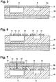
- a film of a plastic composite material in the present case glass fibers arranged in an epoxy resin, is now unwound from a further roll and placed on the arrangement of the fig. 4th hung up. Both are passed through a gap between two heated rollers in order to heat the film of the plastic composite material and to press it against the envelope, ie the filler material 19, in order to laminate the plastic composite material onto the envelope.
- the laminated plastic composite material forms a carrier 9 for the arrangement of fig. 4th , in the present case a rigid carrier 9.
- the low-temperature sintering for forming the mechanical and electrical connection 23 between the contact points 5c and the surface 30 is carried out in this step by the lamination takes place in a temperature range required for this, so that sintering is also triggered at the same time as the lamination.
- a laser beam directed onto the film surface 3u vaporizes predetermined sections of the film 3.
- the remaining sections of the film 3 form conductor tracks 11 and an electrically non-connected film cooling section 13, see FIG. fig. 6th .
- layer 9a being a thermoplastic polymer
- layer 9b being a plastic composite material, in the present case glass fibers arranged in an epoxy resin, see fig. fig. 7th .
- the Figure 9a shows a perspective view of the film 3 with two electronic components 5.1 and 5.2, which are each designed here as so-called bare dies.
- the Figure 9b shows a plan view of the film which does not fall under the claimed invention, the film 3 with the components 5.1 and 5.2 fixed thereon by the adhesive connection.
- the adhesive 20 is applied so that the adhesive connection between the lateral edge 21 and the surface 30 of the film 3 results.
- the adhesive 20 for fixing the component 5.2 is applied punctiformly on the film 3 in the area of the corners of the component 5.2, as also shown in FIG. 9b.
- the Figure 9c shows the corresponding sectional views.
- the possible active surface for electrical contacting of the components 5.1 or 5.2 is not or only insignificantly reduced by the formation of the adhesive connection.
- essentially the entire underside of the components 5.1 or 5.2, ie the contact side 5b, is available for electrical contact with the film 3, as is the upper sides of the components 5.1 and 5.2.
- Fig. 10 to fig. 14th show schematically a section of a conductive film 3 unwound from a roll according to a further example which does not fall under the claimed invention.
- This film 3 has adjustment markings 2 at certain precisely defined points, for example in the form of holes extending through the film 3.
- the film 3 is uncoated on both sides. It is, for example, a copper foil.
- Adhesive 20 is applied to the upper side 30 at certain points which are defined in their position with respect to the adjustment marks 2.
- the application can be done by printing, spraying, dripping or the like.
- Individual spacer elements 31, for example glass spheres of a certain size, can be mixed into the adhesive. With the size of the spacer it is possible to set different thicknesses of the dielectric.
- the adhesive also contains nanoparticles to enable the subsequent low-temperature sintering, preferably a pressureless low-temperature sintering.
- an envelope made of a filler material 19, for example a polymer mass can be applied around the electronic components 5, which envelops individual or all electronic components in a separate or a common envelope.
- This process can trigger the sintering of the nanoparticles contained in the adhesive 20 in order to create the connections 23 (cf. Fig. 4 ) if the process is carried out at a sufficiently high temperature.
- the envelope extends outside the electronic components 5 up to that in the Fig. 10 to fig. 13 upper side 30 of the slide 3.
- the adjustment markings 2 can also be used for dimensioning and arranging the cover made of the polyester compound with respect to the electronic components 5.
- the sheathing envelops components 5 and extends as far as the film 3, and possibly also forms a type of adhesive bond with the film 3, a mechanically stable block is thereby formed.
- the envelope also extends between the contact points, as in FIG Figures 13 and 14 shown.
- the film 3 provided with the covering is laminated to a circuit board carrier 9, which comes to lie on the side of the film 3 on which the electronic components 5 are also arranged (cf. the arrangement according to FIG Fig. 5 ). This, at the latest, triggers the sintering and thus the production of the connections 23.
- the film 3 is now structured on its free side 8, so that conductor tracks are now produced.
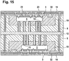
- fig. 15th shows such a further embodiment of an electronic assembly, with practically two assemblies, as in fig. 14th shown, are connected back to back with the interposition of a metallic layer 12, which is arranged between the two circuit board supports 9.
- This metallic layer 12 is used, for example, to dissipate the heat generated in the electronic components 5.
- the two assemblies summarized here differ from the simple assembly of the fig. 14th nor in that on the in fig. 14th
- metallized cooling channels 15 lead through the circuit board carrier 9 to the central cooling layer 12, so that the heat can be dissipated here.
- the fig. 16 to fig. 21st show states during the implementation of the procedure which are approximately the fig. 10 to fig. 14th correspond.
- the illustrated embodiment is a film 33 as the starting material, which is attached to a carrier film 34.
- the carrier film 34 can consist of metal, ceramic or also polymer.
- the conductive foil 33 consists for example of copper and is not coated with nanoparticles.
- connection pads 35 are formed on the carrier film 34 which correspond to the connection points 5c of the electronic components to be fastened.
- Such an electronic component 5 is shown in fig. 18th shown.
- This electronic component 5 is now connected to the connection pads 35 with its connection points 5c. This can be done, for example, by applying adhesive 20 to the connection pads 35 or the sides of the connection points 5c of the electronic component 5 facing them.
- the adhesive 20 is an adhesive with nanoparticles distributed in the adhesive. As a result, an adhesive layer is formed that is present between the connection pads 35 and the connection points 5c of the electronic component 5. In this way, the electronic component 5 is connected to its connection points 5c facing the connection pads 35, namely initially only via an adhesive connection.
- the electronic component 5 can then be surrounded by an envelope made of a filler material 19, again made of polymer compound, which surrounds the entire electronic component 5 including the connection pads 35 and extends as far as the carrier film 34.
- a filler material 19 again made of polymer compound
- the carrier film 34 can then be separated, which is shown in FIG fig. 20th is shown.
- the further treatment of the casing or a lamination and the electronic component 5 contained therein takes place in the manner customary for printed circuit boards. It is essential that the wrapping with the filler material or the lamination a temperature range is reached in which the low-temperature sintering of the nanoparticles contained in the adhesive 20 is triggered in order to create the connections 23 (cf. Fig. 4 ) to produce.
- fig. 20th shows the detachment of the carrier layer 34. Instead of detaching the carrier layer 34, it is also possible not to detach the carrier layer 34, but to structure it further, for example by etching, by removal or the like. This is in fig. 21st shown.
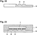
- the fig. 22 and fig. 23 show a further example which does not fall under the claimed invention, wherein a thicker film 36 is used as the starting film, which is then similar to FIG fig. 17th is initially structured on its side facing the electronic components, in order to thereby form connection pads 35. Links in fig. 22nd the initial state of this thicker film 36 is shown, while on the right in FIG fig. 22nd the result of the structuring is shown.
- the electronic component 5 is then placed on the structured film produced in this way in the same way, fastened with the aid of the adhesive 20, as shown in FIG fig. 18th was shown.
- structuring can take place after the electronic component 5 and the casing have been attached.
- the method proposed by the invention makes it possible to achieve a considerably increased use of space on electronic circuit carriers. Additional layers can be produced with components populated in a very small space, both active and passive components.
- the passive and active electronic components can be encapsulated inexpensively, which results in a high level of reliability. Risky mixed techniques, namely soldering, gluing and wire bonding are avoided in production.
- a planar initial structure enables reproducible RF transitions to be achieved. It is of particular advantage that no separate process step is required for the formation of the electrical connections, since this takes place by low-temperature sintering together with the casing or the lamination, and that this simultaneously creates a particularly stable mechanical connection and an electrical connection with a low contact resistance and a short length results, which is advantageous for high frequency applications.
Landscapes
- Health & Medical Sciences (AREA)
- Engineering & Computer Science (AREA)
- General Health & Medical Sciences (AREA)
- Biomedical Technology (AREA)
- Veterinary Medicine (AREA)
- Public Health (AREA)
- Animal Behavior & Ethology (AREA)
- Life Sciences & Earth Sciences (AREA)
- Mechanical Engineering (AREA)
- Heart & Thoracic Surgery (AREA)
- Microelectronics & Electronic Packaging (AREA)
- Otolaryngology (AREA)
- Vascular Medicine (AREA)
- Anesthesiology (AREA)
- Hematology (AREA)
- Neurosurgery (AREA)
- Physics & Mathematics (AREA)
- Acoustics & Sound (AREA)
- Signal Processing (AREA)
- Laminated Bodies (AREA)
- Nuclear Medicine, Radiotherapy & Molecular Imaging (AREA)
- Radiology & Medical Imaging (AREA)
- Cardiology (AREA)
Description
- Die Erfindung betrifft ein Verfahren zum Herstellen einer elektronischen Baugruppe.
- Ein derartiges Verfahren ist bekannt aus
DE 10 2008 009 220 A1 und ausDE 10 2010 014 579 A1 . - Die Druckschrift
DE 10 2011 000 530 A1 offenbart ein Verfahren zur Herstellung einer Halbleiteranordnung. In einem Ausführungsbeispiel wird auf eine Metallfolie eine Paste aufgebracht und in diese Paste ein Halbleiterchip eingedrückt. - Die Druckschrift
JP2008141007 - Die Druckschrift
DE 10 2008 040 488 A1 offenbart eine elektronische Baueinheit und ein Verfahren zu deren Herstellung. - Aufgabe der vorliegenden Erfindung ist es demgegenüber, ein verbessertes Verfahren und eine verbesserte elektronische Baugruppe anzugeben.
- Diese Aufgabe wird verfahrensseitig gelöst durch
- 1.1 Bereitstellen einer elektrisch leitenden Folie, insbesondere einer Trägerfolie,
- 1.2 Bereitstellen mindestens eines elektrischen Bauteils mit mindestens einer elektrischen Kontaktstelle,
- 1.3 Aufbringung eines Klebers zwischen dem elektrischen Bauteil und einer Oberfläche der elektrisch leitenden Folie,
- 1.4 Anordnen des mindestens einen Bauteils mit der mindestens einen elektrischen Kontaktstelle auf der Oberfläche der elektrisch leitenden Folie, und Fixierung des mindestens einen Bauteils durch Ausbildung einer Klebeverbindung zwischen dem elektrischen Bauteil und der Oberfläche,
- 1.5 Bereitstellen eines Trägers, insbesondere aus einem flexiblen Material,
- 1.6 Laminieren der Folie mit dem Träger derart, dass das mindestens eine elektrische Bauteil zwischen Folie und Träger angeordnet ist, und Bilden einer mechanischen und elektrischen Verbindung zwischen der elektrischen Kontaktstelle des mindestens einen elektrischen Bauteils und der elektrisch leitenden Folie durch Niedertemperatursintern von Nanopartikeln, insbesondere aus Gold, Silber, Nickel oder Kupfer oder aus einer Legierung aus diesen Metallen, wobei das Laminieren der Folie gleichzeitig mit dem Niedertemperatursintern erfolgt,
- 1.7 Strukturieren der elektrisch leitenden Folie zu Leiterbahnen undloder Kühlflächen.
- Ausführungsform der Erfindung sind besonders vorteilhaft, da das Laminieren und das Niedertemperatursintern in demselben Prozessschritt im Wesentlichen gleichzeitig erfolgen können. Dies wird einerseits durch die Verwendung von Nanopartikeln ermöglicht, welche ein Niedertemperatursintern in einem Temperaturbereich ermöglichen, der auch für das Laminieren der Folie geeignet ist, und andererseits durch die vorherige Fixierung des mindestens einen elektrischen Bauteils auf der Oberfläche der elektrisch leitenden Folie. Durch diese Fixierung ist sichergestellt, dass sich das elektrische Bauteil an der richtigen Stelle befindet, wenn der Träger für das nachfolgende Laminieren auf die Folie und die im Raum befindlichen Bauteile aufgebracht wird, und dass das Bauteil nicht verrutschen kann.
- Unter einem "elektrischen Bauteil" werden hier insbesondere gehauste und ungehauste elektronische Bauelemente, wie zum Beispiel integrierte Halbleiterchips, zum Beispiel sogenannte Nacktchips ("bare chip" oder "bare die") verstanden sowie auch diskrete elektrische oder elektronische Bauelemente, wie zum Beispiel Kondensatoren.
- Ein solches elektrisches Bauteil hat üblicherweise eine Seite, auf der eine oder mehrere elektrische Kontaktstellen zur elektrischen Kontaktierung des Bauteils vorgesehen sind. Diese Seite des Bauteils wird auch als "aktive Seite" des Bauteils bezeichnet. Insbesondere wenn es sich bei dem Bauteil um ein bare die handelt, sind die elektrischen Kontaktstellen als sogenannte contact pads ausgebildet.
- Bei dem Träger kann es sich um vorimprägnierte Fasern (preimpregnated fibers, das heißt ein sogenanntes Prepreg) handeln, worunter hier eine ungehärtete duroplastische Kunststoffmatrix verstanden wird. Beispielsweise kann es sich bei dem Träger um ein flüssigkristallines Polymer (liquid crystal polymere - LCP) handeln, was besonders vorteilhaft zur Herstellung biokompatibler Implantate ist, oder ein anderes Trägermaterial.
- Nach einer Ausführungsform der Erfindung wird als Ausgangsmaterial eine elektrisch leitende Folie verwendet, deren Oberfläche mit Nanopartikeln beschichtet ist. Das mindestens eine elektrische Bauteil wird dann auf der Oberfläche der elektrisch leitenden Folie durch einen Kleber fixiert, der außerhalb der elektrischen Kontaktstellen des Bauteils aufgebracht wird. Vorzugsweise handelt es sich bei dem Kleber um einen nicht leitfähigen Kleber, das heißt ein sogenanntes non-conducting-adhesive (NCA) oder eine non-conducting paste (NCP). Wenn es sich beispielsweise bei dem elektrischen Bauteil um ein bare die handelt, welches außerhalb der elektrischen Kontaktstellen von einer Passivierungsschicht umgeben ist, so wird die Klebeverbindung mithilfe dieses Klebers zwischen der Passivierungsschicht und der Oberfläche der elektrisch leitenden Folie hergestellt.
- Nach einer Ausführungsform der Erfindung wird als Ausgangsmaterial eine elektrisch leitende Folie verwendet, deren Oberfläche nicht mit Nanopartikeln beschichtet sein muss. In diesem Fall wird ein Kleber verwendet, der die Nanopartikel beinhaltet. Der Kleber wird auf die mindestens eine elektrische Kontaktstelle des elektrischen Bauteils aufgebracht, um das elektrische Bauteil auf der Oberfläche der elektrisch leitenden Folie zu fixieren. Anschließend wird der Träger aufgebracht, um die Folie mit dem Träger zu laminieren und gleichzeitig die Niedertemperatursinterung durchzuführen. Hierbei versintern die in der Klebeverbindung beinhalteten Nanopartikel. Diese Ausführungsform des erfindungsgemäßen Verfahrens ist besonders vorteilhaft, da durch die Aufbringung des Klebers auch gleichzeitig die Nanopartikel aufgebracht werden, die für das anschließende Niedertemperatursintern erforderlich sind.
- Nach einer Ausführungsform der Erfindung wird das Niedertemperatursintern als "druckloses" Niedertemperatursintern durchgeführt. Unter "drucklos" wird hierbei verstanden, dass das Niedertemperatursintern nicht bei den üblicherweise anzuwendenden hohen Drücken von zum Beispiel 200 bar, d.h. 2000 kPa, durchgeführt wird, sondern bei einem wesentlich geringeren Druck, wie er auch für das Laminieren verwendet wird, das heißt bei einem Druck von beispielsweise 15 - 20 bar. , d.h. 1500-2000 kPa.
- Entsprechende Kleber oder Pasten, die Nanopartikel für eine solche drucklose Niedertemperatursinterung enthalten sind an sich aus dem Stand der Technik bekannt, wie z.B. aus
DE 10 2008 039 828 A1 , und sind kommerziell von der Firma Heraeus unter dem Handelsnamen mAgic Adhesive bzw. mAgic Paste erhältlich. - Hierdurch wird ein besonders effizientes und Material sparendes Herstellungsverfahren ermöglicht, da die Menge der eingesetzten Nanopartikel minimiert werden kann. Außerdem ist die so hergestellte Verbindung besonders mechanisch stabil und hat gut elektrische Kontakteigenschaften aufgrund der kovalenten Bindungen der Nanopartikel, die zu einem geringen Übergangswiderstand führen.
- Nach einer Ausführungsform der Erfindung ist die Größe der Nanopartikel so gewählt, dass diese bei Raumtemperatur chemisch relativ inert sind, sodass bei Raumtemperatur keine spontane Versinterung erfolgt. Andererseits ist die Größe der Nanopartikel hinreichend klein gewählt, sodass in dem für das Laminieren erforderlichen Temperaturbereich die Reaktionsfähigkeit der Nanopartikel im Vergleich zu makroskopischen Partikeln bereits so weit erhöht ist, dass es zur Ausbildung kovalenter chemischer Verbindungen zwischen den Nanopartikeln kommt, sodass diese also miteinander versintern.
- Nach einer Ausführungsform der Erfindung kann es sich bei dem Kleber um ein LCP handeln. Dies ist besonders vorteilhaft, wenn auch der Träger durch ein LCP gebildet wird, insbesondere im Hinblick auf die thermische Belastbarkeit und die Langzeitstabilität der resultierenden elektronischen Baugruppe, was besonders für Anwendungen im medizinischen Bereich, insbesondere für Implantate, vorteilhaft ist.
- In einem weiteren Aspekt betrifft die Erfindung ein Verfahren zum Herstellen einer elektronischen Baugruppe, bei dem vor dem Laminieren der Folie mit dem Träger das auf der elektrisch leitenden Folie angeordnete mindestens eine Bauteil mit einem Füllmaterial aus einem Polymer umhüllt wird, wobei bereits bei diesem Schritt des Umhüllens das Niedertemperatursintern erfolgt. Dies ist besonders vorteilhaft, wenn das resultierende Zwischenprodukt in einem diskontinuierlichen Prozess von einer Fertigungsstation zu einer anderen transportiert werden muss sowie auch für die mechanische Stabilität der resultierenden elektronischen Baugruppe.
- In einem weiteren Aspekt betrifft die Erfindung eine elektronische Baugruppe, die nach einem erfindungsgemäßen Verfahren hergestellt worden ist. Insbesondere kann es sich hierbei um ein implantat handeln, wie zum Beispiel ein Elektronikmodul für eine Insulinpumpe, einen Herzschrittmacher oder ein implantierbares Hörgerät.
- Vorteilhaft erfolgt das Bereitstellen der Folie durch das Bereitstellen einzelner, zugeschnittener Folienabschnitte oder durch das Bereitstellen einer Endlosfolie von einer Rolle.
- Bevorzugt erfolgt das Bereitstellen des mindestens einen elektrischen Bauteils durch Bereitstellen desselben auf einer Endlosfolie oder Bereitstellen in einem Magazin.
- Vorteilhaft erfolgt das Anordnen des mindestens einen elektrischen Bauteils automatisiert durch einen Bestückungsroboter oder von Hand, insbesondere mit Hilfe von Schablonen oder Positionsmarkern in bzw. auf der Folie.
- Das Bereitstellen des Trägers kann durch Bereitstellen einzelner, zugeschnittener Trägerabschnitte oder durch Bereitstellen eines Endlosträgers von einer Rolle erfolgen.
- Vorzugsweise erfolgt das Laminieren der Folie mit dem Träger durch Ausüben eines Anpressdruckes auf die Folie in Richtung des Trägers, insbesondere unter gleichzeitiger Wärmeeinwirkung.
- Vorteilhaft erfolgt das Strukturieren der elektrisch leitenden Folie zu Leiterbahnen und ggfs. Kühlflächen durch Direktstrukturierung, z. B. mit einem Laser, oder durch Erzeugen einer Positiv- oder Negativmaske und anschließendem Ätzen.
- Vorteilhaft wird die Folie mit dem Träger und dem mindestens einen elektrischen Bauteil nach der Strukturierung der Folie auf einer Rolle aufgewickelt.
- In Weiterbildung der Erfindung kann vorgesehen sein, dass ein Umhüllen des mindestens einen elektrischen Bauteils nach der Anordnung des Bauteils auf der Folie mit einem Füllmaterial aus einem Polymer, insbesondere einem Thermoplast, Duroplast oder einem Elastomer erfolgt.
- Vorteilhaft erfolgt das Füllen des Füllmaterials in eine vorbestimmte Form, insbesondere durch Giessen, Schäumen, Extrudieren oder Laminieren.
- In Weiterbildung der Erfindung kann vorgesehen sein, dass ein Erzeugen mindestens einer weiteren Trägerschicht auf den durch Strukturierung erzeugten Leiterbahnen erfolgt, wobei diese bevorzugt isolierend und/oder dieelektrisch ist und/oder weitere Leiterbahnen enthält.
- Insbesondere kann nach dem Schritt 1.6 ein Aufbringen mindestens einer Verstärkungsschicht, vorzugsweise mehrerer Verstärkungsschichten, auf den Träger oder die Trägerschicht erfolgen. Es kann alternativ auch vorgesehen sein, dass der Träger ggfs. nach dem Schritt 1.6 entfernt wird.
- In Weiterbildung der Erfindung kann ein Zuschneiden des Trägers in eine vorbestimmte Form zum Bilden der elektronischen Baugruppe, insbesondere vor und/oder nach dem Laminieren mit der Leiterplatte im Schritt 1.6. erfolgen.
- Dabei kann die elektrisch leitende Folie aus Metall, insbesondere Kupfer, elektrisch leitfähigem Kunststoff oder elektrisch leitfähiger Keramik bestehen, auf deren Oberfläche ggfs. zumindest bereichsweise eine Schicht aus Silber oder einer Silberverbindung und/oder eine dreidimensionale Struktur aus metallischen Nanopartikeln vorhanden ist und ggfs. durch eine Trägerfolie verstärkt ist.
- Insbesondere kann vorgesehen sein, dass die elektrisch leitende Folie auf der dem mindestens einem elektrischen Bauteil zugewandten Seite glatt oder angerauht ist oder eine Höckerstruktur aufweist.
- Es kann vorgesehen sein, dass das mindestens eine elektrische Bauteil ein passives oder aktives Bauelement, insbesondere ein Chip, ist, wobei es vorzugsweise außerhalb der Kontaktstellen mit einem Schutzüberzug, insbesondere einem Lack, d.h. einer sog. Passivierungsschicht versehen ist.
- In Weiterbildung kann vorgesehen sein, dass der Schutzüberzug elektrisch isolierend und/oder ein Dieelektrikum ist.
- Vorteilhaft kann der Träger eine Folie, insbesondere aus Metall, Kunststoff oder Keramik sein, eine Matte aus Naturmaterialien, wie z. B. Pflanzenfasern, ein Lederabschnitt, ein Textilabschnitt oder ein Abschnitt aus einem sonstigen Gewebe oder Verbundwerkstoff sein oder eine Leiterplatte, ein Keramikträger oder ein Glasträger sein.
- In Weiterbildung der Erfindung kann vorgesehen sein, dass dem Träger eine Verstärkungsschicht zugeordnet ist und insbesondere aus Metall, Kunststoff oder Keramik sein kann, aus Naturmaterialien, wie z. B. Pflanzenfasern, aus Leder, aus Textil oder aus einem sonstigen Gewebe oder Verbundwerkstoff sein kann oder eine Leiterplatte, ein Keramikträger oder ein Glasträger sein kann.
- Das mindestens eine elektrische Bauteil kann mindestens eine Kontaktseite aufweisen, in der jeweils mindestens eine elektrische Kontaktstelle angeordnet ist, wobei vorzugsweise die mindestens eine elektrische Kontaktstelle plan mit der entsprechenden Kontaktseite ist.
- Vorteilhaft besteht die Kontaktstelle aus Kupfer oder einer Kupferverbindung, auf deren Oberfläche ggfs. eine Schicht aus Silber oder einer Silberverbindung und/oder eine dreidimensionale Struktur aus metallischen Nanopartikeln vorhanden sein kann.
- In Weiterbildung kann vorgesehen sein, dass an dem mindestens einem elektrischen Bauteil ein Abschnitt der elektrisch leitenden Folie als Wärme abführender Kontaktbereich gebildet ist (Folienkühlabschnitt).
- In Weiterbildung der Erfindung kann vorgesehen sein, dass ein Kühlkörper oder ein Kühlkanal mit dem Folienkühlabschnitt und/oder dem mindestens einem elektronischen Bauteil verbunden ist.
- Weitere Einzelheiten, Merkmale und Vorzüge der Erfindung ergeben sich aus den Patentansprüchen, deren Wortlaut durch Bezugnahme zum Inhalt der Beschreibung gemacht wird, der folgenden Beschreibung bevorzugter Ausführungsformen der Erfindung sowie anhand der Zeichnungen. Hierbei zeigen:
-
fig. 1 schematisch die Seitenansicht einer elektrisch leitenden Folie als Ausgangsmaterial für das Verfahren; -
fig. 2 schematisch einen Querschnitt eines elektrischen Bauteils; -
fig. 2a einen vergrößerten Ausschnitt derfig. 2 ; -
fig. 2b eine vergrößerte Darstellung einer Kontaktstelle des Bauteils derfig. 2a ; -
fig. 3 eine Seitenansicht der Folie derfig. 1 mit zwei darauf angeordneten Bauteilen; -
fig. 4 die Anordnung derfig. 3 , wobei zusätzlich ein Füllmaterial aufgebracht ist; -
fig. 5 die Anordnung derfig. 4 , wobei zusätzlich ein Träger auflaminiert ist; -
fig. 6 die Anordnung derfig. 5 , wobei zusätzlich Leiterbahnen und ein Folienkühlabschnitt angeordnet sind; -
fig. 7 die Anordnung derfig. 6 , wobei zusätzlich Leiterbahnen und ein Folienkühlabschnitt angeordnet sind, wobei aber der Träger 9 wieder entfernt und eine Trägerschicht 9a mit einer weiteren Verstärkungsschicht 9b auf der Seite der Leiterbahnen auflaminiert wurde; und -
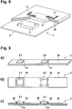
fig. 8 schematische Ansicht einer elektronischen Baugruppe -
fig. 9 eine perspektivische Darstellung von Klebeverbindungen, -
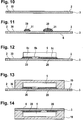
fig. 10 schematisch die Seitenansicht einer leitenden Folie als Ausgangsmaterial für eine weitere Ausführungsform eines erfindungsgemäßen Verfahrens; -
fig. 11 den gleichen Abschnitt der Folie mit aufgebrachten Kleberpunkten; -
fig. 12 die gleiche Ansicht mit zwei mithilfe der Kleberpunkte verklebten elektronischen Bauteilen; -
fig. 13 den Zustand der Herstellung nach dem Aufbringen einer Umhüllung; -
fig. 14 den Zustand nach dem Zuschneiden einer elektronischen Baugruppe; -
fig. 15 den Endzustand einer nach dem Verfahren hergestellten Mehrlagenleiterplatte; -
fig. 16 die schematische Seitenansicht eines Ausgangsmaterials nach einer weiteren Ausführungsform des erfindungsgemässen Verfahrens; -
fig. 17 den Zustand nach einem weiteren Verfahrensschritt; -
fig. 18 den Zustand nach einem weiteren Verfahrensschritt; -
fig. 19 einen weiteren Verfahrensschritt; -
fig. 20 das Abziehen der Trägerfolie; -
fig. 21 eine derfig. 20 entsprechende Darstellung bei einer Abwandlung; -
fig. 22 eine Ausgangssituation bei einer nochmals weiteren Ausführungsform; -
fig. 23 den derfig. 21 entsprechenden Zustand der Ausführungsform nachfig. 22 ; - Im Weiteren werden einander entsprechende oder identische Elemente der verschiedenen Ausführungsformen jeweils mit denselben Bezugszeichen gekennzeichnet.
fig. 1 zeigt schematisch einen Ausschnitt einer Seitenansicht einer von einer Rolle abgewickelten, elektrisch leitenden Folie 3 aus Kupfer. Eine Folienoberfläche 3o , welche nachher einem elektrischen Bauteil 5 zugewandt ist, ist mit einer gleichmäßigen Beschichtung von Nanopartikeln, beispielsweise Silberpartikeln einer Partikelgröße von ca. 20-300 nm oder einer silberhaltigen Legierung versehen. Die Folie 3 ist an der der Seite 3o gegenüberliegenden Seite durch eine Trägerfolie 3a verstärkt, die auf die Folie 3 auflaminiert ist und aus einem Polymer besteht.
fig. 2 zeigt schematisch ein elektrisches Bauteil 5 , vorliegend einen Chip, in einer Schnittansicht. Das Bauteil 5 ist an allen Seiten von einer Schutzschicht 5a aus elektrisch isolierendem Lack überzogen, d.h. einer sog. Passivierungsschicht. Das Bauteil 5 weist eine Kontaktseite 5b, die auch als aktive Seite bezeichnet wird, mit zwei Kontaktstellen 5c für die elektrische Kontaktierung mit der Folie 3 auf, die von der aufgetragenen Schutzschicht 5a ausgespart sind. Zusätzlich kann das Bauteil 5 weitere Kontaktstellen haben, wie z.B. an dessen Kante 21 oder an der Oberseite 22. Die Oberflächen der Kontaktstellen 5c sind, wie ausfig. 2b ersichtlich, mit einer Schicht Silber (oder einer silberhaltigen Legierung) beschichtet, nämlich mit Nanopartikeln 37. Die Nanopartikel können teilweise in die Kontaktstellen 5c hinein diffundieren, was einen besonders geringen elektrischen Übergangswiderstand ergibt. Die Bauteile 5 werden von einer von einer Rolle abgewickelten Folie bereitgestellt, auf der sie zueinander beabstandet angeordnet sind. Beispielsweise handelt es sich bei dem Bauteil 5 um ein bare die, wobei die Kontaktstellen 5c dann als sog. contact pads ausgebildet sind. - Ein Roboterarm greift jeweils ein oder mehrere Bauteile 5 von der Folie und setzt diese an definierten Stellen auf der beschichteten Oberfläche 3o der Folie 3 auf. Dabei wird ein Kleber zwischen dem Bauteil 5 und der Oberfläche 30 der elektrisch leitenden Folie aufgebracht, um das Bauteil durch Ausbildung einer Klebeverbindung zu fixieren, wobei es sich bei der Verbindung 7 um eine Klebeverbindung handelt.
- Der Kleber wird vor dem Absetzen eines der Bauteile 5 auf die Oberfläche 30 der Folie aufgebracht. In einem Beispiel, das nicht unter die beanspruchte Erfindung fällt, kann der Kleber, beispielsweise ebenfalls robotisch, außerhalb der elektrischen Kontaktstellen 5c auf die aktive Seite, d.h. die Kontaktseite 5b des Bauteils 5 aufgebracht werden. Ein weiteres Beispiel, das nicht unter die beanspruchte Erfindung fällt ist, dass zunächst das Bauteil von dem Roboterarm auf der Oberfläche 30 der elektrisch leitenden Folie positioniert wird, um das Bauteil dort anzuordnen, und dass anschließend der Kleber zur Herstellung der Klebeverbindung aufgebracht wird, beispielsweise indem der Kleber entlang der seitlichen Kante des Bauteils aufgebracht wird (vgl. hierzu auch die Beispiele gemäß
Fig. 9 ). - Die auf diese Weise hergestellte Klebeverbindung fixiert die Bauteile 5 mechanisch auf der Folie 3 ohne sie elektrisch mit ihr zu kontaktieren. Vorzugsweise wird bei diesem Beispiel der Kleber 20 (vgl.
Fig. 9 ) außerhalb der elektrischen Kontaktstellen 5c aufgebracht, um die anschließende Ausbildung der mechanischen und elektrischen Verbindung 23 (vgl.Fig. 4 ) durch das Niedertemperatursintern nicht zu behindern, zumal der Kleber 20 bei diesem Beispiel <eine metallischen Nanopartikel enthält.
fig. 3 zeigt die Anordnung von zwei derartig befestigten Bauteilen 5 auf der Folie 3. Nach einer Ausführungsform der Erfindung wird von einer weiteren Rolle eine Folie eines thermoplastischen Polymers abgerollt und auf die Anordnung derfig. 3 aufgelegt. Beides wird durch einen Spalt zwischen zwei erwärmten Walzen geführt, um die Folie des thermoplastischen Polymers zu erwärmen und diese gegen die Folie 3 zu drücken, um die Bauteile 5 zu umhüllen. Dadurch entsteht eine Umhüllung der Bauteile 5 mit einem Füllmaterial 19 (dem thermoplastischen Polymer) auf der Folie 3, die die Bauteile 5 vor Umwelteinflüssen schützt, wie infig. 4 dargestellt. - Bei diesem Schritt kann es bereits zu der Niedertemperatursinterung, d.h. zur Ausbildung einer mechanischen und elektrischen Verbindung 23 zwischen den Kontaktstellen 5c und der Oberfläche 30 kommen, wenn die Walzen hinreichend warm sind. Von einer weiteren Rolle wird nun eine Folie eines Kunststoffverbundmaterials, vorliegend in einem Epoxyharz angeordnete Glasfasern, abgewickelt und auf die Anordnung der
fig. 4 aufgelegt. Beides wird durch einen Spalt zwischen zwei erwärmten Walzen geführt, um die Folie des Kunststoffverbundmaterials zu erwärmen und diese gegen die Umhüllung, d.h. das Füllmaterial 19 zu drücken, um das Kunststoffverbundmaterial auf die Umhüllung aufzulaminieren. - Wie in
fig. 5 dargestellt, bildet das auflaminierte Kunststoffverbundmaterial einen Träger 9 für die Anordnung derfig. 4 , vorliegend einen starren Träger 9. Nach der Erfindung wird bei diesem Schritt die Niedertemperatursinterung zur Ausbildung der mechanischen und elektrischen Verbindung 23 zwischen den Kontaktstellen 5c und der Oberfläche 30 durchgeführt, indem die Laminierung in einem dafür erforderlichen Temperaturbereich erfolgt, so dass gleichzeitig mit der Laminierung auch die Sinterung ausgelöst wird. - Ein auf die Folienoberfläche 3u gerichteter Laserstrahl verdampft vorbestimmte Abschnitte der Folie 3 . Die verbleibenden Abschnitte der Folie 3 bilden Leiterbahnen 11 und einen elektrisch nicht angebundenen Folienkühlabschnitt 13, s.
fig. 6 . - Auf die in
fig. 6 obere Seite werden weitere Schichten 9a und 9b auflaminiert, wie oben beschrieben, wobei die Schicht 9a ein thermoplastisches Polymer ist und die Schicht 9b ein Kunststoffverbundmaterial, vorliegend in einem Epoxyharz angeordnete Glasfasern, ist, s.fig. 7 . In diesen Schichten ist ein Kühlkanal 15 durch Bohren gebildet, der mit einem Kühlkörper 17 verbunden ist. - Die laminierten Schichten 9 , 9a , 9b und 19 mit den darin befindlichen, elektrischen Bauteilen 5 werden durch einen Laserstrahl in einzelne elektronische Baugruppen getrennt. In
fig. 8 ist eine teilweise weggebrochene perspektivische Ansicht der auf diese Weise hergestellten Baugruppe 1 dargestellt, die nun für ihren Einsatz, bspw. in Mobiltelephonen, zur Verfügung steht. - Die
Figur 9a zeigt in perspektivischer Ansicht die Folie 3 mit zwei elektronischen Bauteilen 5.1 und 5.2, die hier jeweils als sogenannte bare dies ausgebildet sind. - Die
Figur 9b zeigt eine Draufsicht auf die Folie, die nicht unter die beanspruchte Erfindung fällt, wobei die Folie 3 mit den daran durch die Klebeverbindung fixierten Bauteilen 5.1 und 5.2. Zur Ausbildung der Klebeverbindung zwischen dem Bauteil 5.1 und der Folie 3 wird entlang der seitlichen Schnittkante 21 (vgl. auchFig. 2 ), entlang derer das Bauteil 5.1 aus einem Wafer herausgeschnitten worden ist, der Kleber 20 aufgebracht, sodass die Klebeverbindung zwischen der seitlichen Kante 21 und der Oberfläche 30 der Folie 3 resultiert. - Dagegen wird der Kleber 20 zur Fixierung des Bauteils 5.2 auf der Folie 3 punktförmig im Bereich der Ecken des Bauteils 5.2 aufgebracht, wie ebenfalls in der Figur 9b dargestellt.
- Die
Figur 9c zeigt die entsprechenden Schnittansichten. Besonders vorteilhaft ist hier in beiden Fällen, dass die mögliche aktive Fläche für eine elektrische Kontaktierung der Bauelemente 5.1 bzw. 5.2 durch die Ausbildung der Klebeverbindung nicht bzw. nur unwesentlich verringert wird. Insbesondere steht trotz der Ausbildung der Klebeverbindung im Wesentlichen die gesamte Unterseite der Bauteile 5.1 bzw. 5.2, d.h. die Kontaktseite 5b, für eine elektrische Kontaktierung mit der Folie 3 zur Verfügung sowie auch die Oberseiten der Bauteile 5.1 und 5.2. -
Fig. 10 bis fig. 14 zeigen schematisch einen Ausschnitt aus einer von einer Rolle abgewickelten leitfähigen Folie 3 gemäß einem weiteren Beispiel, das nicht unter die beanspruchte Erfindung fällt. Diese Folie 3 hat an bestimmten genau definierten Stellen Justagemarkierungen 2 , beispielsweise in Form von durch die Folie 3 hindurchgehende Löchern. Die Folie 3 ist auf beiden Seiten unbeschichtet. Es handelt sich beispielsweise um eine Kupferfolie. - Auf der Folie 3 wird auf der in den
fig. 10 bis fig. 13 oberen Seite 30 an bestimmten Stellen, die in ihrer Position gegenüber den Justagemarkierungen 2 festgelegt sind, Kleber 20 aufgebracht. Das Aufbringen kann durch Drucken, Spritzen, Tropfen oder dergleichen geschehen. In dem Kleber können einzelne Abstandselemente 31, beispielsweise Glaskugeln einer bestimmten Größe, eingemischt sein. Mit der Größe der Spacer ist es möglich, verschiedene Dicken des Dielektrikums einzustellen. Der Kleber beinhaltet ferner Nanopartikel zur Ermöglichung des nachfolgenden Niedertemperatursinterns, vorzugsweise eines drucklosen Niedertemperatursinterns. - In einem weiteren Verfahrensschritt werden nun elektronische Bauteile mithilfe von geeigneten Einrichtungen auf die Stellen aufgesetzt, an denen vorher der Kleber 20 aufgebracht wurde, so dass die Kontaktstellen 5c der Bauteile mit dem Kleber 20 in Berührung kommen; dies ist in der
fig. 12 exemplarisch für ein Bauteil 5 gezeigt, welches zwei Kontaktstellen 5c an dessen Kontaktseite 5b hat. - Diese elektronischen Bauteile 5 werden angedrückt, so dass die Kleberpunkte des Klebers 20 verquetscht werden und nur die Kontaktstellen 5c der elektronischen Bauteile 5 abdecken und gegenüber der Folie 3 verkleben. Dieser Zustand ist in
fig. 12 dargestellt. Je nach Art des verwendeten Klebers können weitere Maßnahmen ergriffen werden, um das Aushärten des Klebers zu beschleunigen, beispielsweise eine zusätzliche oder ausschließliche UV-Härtung. - Anschließend kann in einem weiteren Verfahrensschritt, der nicht unbedingt erforderlich ist, um die elektronischen Bauteile 5 herum eine Umhüllung aus einem Füllmaterial 19, z.B. einer Polymermasse aufgebracht werden, die einzelne oder alle elektronischen Bauelemente in einer jeweils separaten oder einer gemeinsamen Umhüllung umhüllt. Durch diesen Vorgang kann die Sinterung der in dem Kleber 20 beinhalteten Nanopartikel ausgelöst werden, um die Verbindungen 23 (vgl.
Fig. 4 ) herzustellen, wenn der Vorgang bei einer ausreichend hohen Temperatur durchgeführt wird. - Die Umhüllung reicht außerhalb der elektronischen Bauteile 5 bis zu der in den
Fig. 10 bis fig. 13 oberen Seite 30 der Folie 3 . Auch zur Dimensionierung und Anordnung der Umhüllung aus der Polyestermasse gegenüber den elektronischen Bauelementen 5 können die Justagemarkierungen 2 dienen. - Da die Umhüllung Bauteile 5 umhüllt und bis zur Folie 3 reicht, gegebenenfalls auch mit der Folie 3 eine Art Verklebung eingeht, ist dadurch ein mechanisch stabiler Block gebildet. Vorzugsweise erstreckt sich die Umhüllung auch zwischen den Kontaktstellen, wie in der
Fig. 13 und 14 gezeigt. - Anschließend an den Verfahrensschritt, dessen Ergebnis in
fig. 13 dargestellt wurde, kann nun die elektronische Baugruppe zugeschnitten werden, das heißt aus der Folie 2 herausgeschnitten werden. Nun wird das Ergebnis des bisherigen Verfahrens umgedreht, so dass jetzt die freie Seite 8 der Folie 2 nach oben zu liegen kommt. Dies wird durch die Umhüllung und die damit verbundene Stabilisierung des in derFig. 13 gezeigten Zwischenprodukts erleichtert, insbesondere der möglicherweise erforderliche Transport zwischen verschiedenen Fertigungsstationen. - In einem weiteren Schritt wird die mit der Umhüllung versehene Folie 3 mit einem Leiterplattenträger 9 laminiert, der auf der Seite der Folie 3 zu liegen kommt, auf der auch die elektronischen Bauteile 5 angeordnet sind (vgl. die Anordnung gemäß
Fig. 5 ). Spätestens hierdurch wird die Sinterung und damit die Herstellung der Verbindungen 23 ausgelöst. - In einem weiteren Schritt wird nun die Folie 3 auf ihrer freien Seite 8 strukturiert, so dass jetzt Leiterbahnen erzeugt sind.
- Diese elektronische Baugruppe kann aber weiterverarbeitet und weiter ausgestaltet werden.
fig. 15 zeigt eine solche weitere Ausgestaltung einer elektronischen Baugruppe, wobei praktisch zwei Baugruppen, wie infig. 14 dargestellt, Rücken an Rücken miteinander verbunden werden unter Zwischenlage einer metallischen Schicht 12 , die zwischen den beiden Leiterplattenträgern 9 angeordnet ist. Diese metallische Schicht 12 dient beispielsweise zur Wärmeabfuhr der in den elektronischen Bauteilen 5 erzeugten Wärme. - Die beiden hier zusammengefassten Baugruppen unterscheiden sich von der einfachen Baugruppe der
fig. 14 noch darin, dass auf die infig. 14 noch obere metallische Schicht, d.h. die Folie 3, unter Zwischenlage einer Isolierungsschicht 32 eine weitere metallische leitende Schicht 14 aufgebracht ist, die durch Öffnungen in der Isolierungsschicht 32 wiederum Kontakte mit Leiterbahnen der ursprünglich oberen leitenden Schicht 2 herstellt. - Von der nicht aktiven Seite der elektronischen Bauteile 5 führen metallisierte Kühlkanäle 15 durch den Leiterplattenträger 9 hindurch zu der mittleren Kühlschicht 12, so dass die Wärme hier abgeleitet werden kann.
- In
fig. 15 ist als Beispiel, das nicht unter die beanspruchte Erfindung fällt, gezeigt, dass die obere der beiden Lagen elektronische Bauteile 5 ohne eine Umhüllung aufweist, während die untere umgedrehte Anordnung eine Umhüllung enthält. - In den
fig. 16 bis fig. 21 wird ein Beispiel, das nicht unter die beanspruchte Erfindung fällt dargestellt. Diefig. 16 bis fig. 21 zeigen Zustände bei der Durchführung des Verfahrens, die etwa denfig. 10 bis fig. 14 entsprechen. - Während in
fig. 10 eine beidseits unbeschichtete Folie 3 als Ausgangsmaterial verwendet wird, verwendet die in denfig. 16 bis fig. 21 dargestellte Ausführungsform als Ausgangsmaterial eine Folie 33 , die an einer Trägerfolie 34 angebracht ist. Die Trägerfolie 34 kann aus Metall, aus Keramik oder auch aus Polymer bestehen. Die leitende Folie 33 besteht beispielsweise aus Kupfer und ist nicht mit Nanopartikeln beschichtet. - In einem ersten Verfahrensschritt wird die leitende Folie 33 in der Weise strukturiert, dass Anschlusspads 35 auf der Trägerfolie 34 ausgebildet werden, die den Anschlussstellen 5c der zu befestigenden elektronischen Bauteile entsprechen.
- Ein solches elektronisches Bauteil 5 ist in
fig. 18 dargestellt. Dieses elektronische Bauteil 5 wird nun mit seinen Anschlussstellen 5c mit den Anschlusspads 35 verbunden. Dies kann beispielsweise dadurch geschehen, dass auf die Anschlusspads 35 oder die diesen zugewandten Seiten der Anschlussstellen 5c des elektronischen Bauteils 5 Kleber 20 aufgebracht wird. - Bei dem Kleber 20 handelt es sich um einen Kleber mit in dem Kleber verteilten Nanopartikeln. Dadurch wird eine Klebschicht gebildet, die jeweils zwischen den Anschlusspads 35 und den Anschlussstellen 5c des elektronischen Bauelements 5 vorhanden ist. Auf diese Weise wird das elektronische Bauteil 5 mit seinen Anschlussstellen 5c den Anschlußpads 35 zugewandt mit diesen verbunden, nämlich zunächst nur über eine Klebeverbindung.
- Anschließend kann das elektronische Bauteil 5 mit einer Umhüllung aus einem Füllmaterial 19 , wiederum aus Polymermasse, umgeben werden, die das gesamte elektronische Bauteil 5 einschließlich der Anschlusspads 35 umgibt und bis zu der Trägerfolie 34 reicht. Das Ergebnis ist in
fig. 19 dargestellt. - Anschließend kann die Trägerfolie 34 abgetrennt werden, was in
fig. 20 gezeigt ist. Die weitere Behandlung der Umhüllung oder einer Laminierung und des darin enthaltenen elektronischen Bauelements 5 geschieht in der bei Leiterplatten üblichen Weise. Wesentlich ist, dass bei der Umhüllung mit dem Füllmaterial oder der Laminierung ein Temperaturbereich erreicht wird, im dem die Niedertemperatursinterung der in dem Kleber 20 beinhalteten Nanopartikel ausgelöst wird, um die Verbindungen 23 (vgl.Fig. 4 ) herzustellen.
fig. 20 zeigt das Ablösen der Trägerschicht 34 . Anstelle des Ablösens der Trägerschicht 34 ist es auch möglich, die Trägerschicht 34 nicht abzulösen, sondern weiter zu strukturieren, beispielsweise durch Ätzen, durch Abtragen oder dergleichen. Dies ist infig. 21 dargestellt. - Die
fig. 22 und fig. 23 zeigen ein weiteres Beispiel, das nicht unter die beanspruchte Erfindung fällt, wobei als Ausgangsfolie eine dickere Folie 36 verwendet wird, die dann ähnlich wie infig. 17 auf ihrer den elektronischen Bauteilen zugewandten Seite zunächst strukturiert wird, um dadurch Anschlusspads 35 zu bilden. Links infig. 22 ist der Ausgangszustand dieser dickeren Folie 36 dargestellt, während rechts infig. 22 das Ergebnis der Strukturierung dargestellt ist. - Auf die so hergestellte strukturierte Folie wird dann das elektronische Bauteil 5 in der gleichen Weise aufgesetzt, mit Hilfe des Kleber 20 befestigt, wie dies in
fig. 18 dargestellt wurde. Auch hier kann nach dem Befestigen des elektronischen Bauteils 5 und der Umhüllung eine Strukturierung erfolgen. - Die elektronischen Baugruppen, wie sie in
fig. 20, fig. 21 undfig. 23 dargestellt sind, können dann in der gleichen Weise zu Mehrlagenbaugruppen zusammengefasst werden, wie dies bei der ersten Ausführungsform beschrieben wurde. - Das von der Erfindung vorgeschlagene Verfahren ermöglicht es, auf elektronischen Schaltungsträgern eine erheblich gesteigerte Flächennutzung zu verwirklichen. Es können zusätzliche Lagen mit auf engstem Raum bestückten Bauelementen hergestellt werden, sowohl aktiven als auch passiven Bauelementen. Die passiven und aktiven elektronischen Bauelemente können kostengünstig verkapselt werden, wodurch eine hohe Zuverlässigkeit erreicht wird. Es werden risikoreiche Mischtechniken, nämlich Löten, Kleben und Drahtbonden in der Fertigung vermieden. Durch eine planare Ausgangsstruktur lassen sich reproduzierbare HF-Übergänge verwirklichen. Von besonderem Vorteil ist, dass kein gesonderter Prozessschritt für die Ausbildung der elektrischen Verbindungen erforderlich ist, da dieses durch Niedertemperatursinterung zusammen mit der Umhüllung oder der Laminierung erfolgt, und dass hierdurch gleichzeitig eine besonders stabile mechanische Verbindung und eine elektrische Verbindung mit einem geringen Übergangswiderstand sowie einer geringen Länge resultiert, was für Hochfrequenzanwendungen vorteilhaft ist.
-
- 1:
- elektronische Baugruppe
- 2:
- Justagemarkierung
- 3:
- elektrisch leitende Folie
- 3a:
- Trägerfolie
- 3o:
- obere Seite der elektrisch leitenden Folie
- 3u:
- untere Seite der elektrisch leitenden Folie
- 5:
- elektrisches Bauteil
- 5a:
- Schutzschicht
- 5b:
- Kontaktseite
- 5c:
- elektrische Kontaktstelle
- 8:
- freie Seite
- 9:
- Träger
- 9a:
- Trägerschicht
- 9b:
- Verstärkungsschicht
- 11:
- Leiterbahnen
- 12:
- metallische Schicht
- 13:
- Folienkühlabschnitt
- 14:
- Schicht
- 15:
- Kühlkanal
- 17:
- Kühlkörper
- 19:
- Füllmaterial
- 20:
- Kleber
- 21:
- Kante
- 22:
- Oberseite
- 23:
- Verbindung
- 30:
- obere Seite
- 31:
- Abstandselement
- 32:
- Isolierungsschicht
- 33:
- Folie
- 34:
- Trägerfolie
- 35:
- Anschlusspads
- 36:
- Folie
- 37:
- Nanopartikel
Claims (13)
- Verfahren zum Herstellen einer elektronischen Baugruppe (1)mit den Schritten:1.1 Bereitstellen einer elektrisch leitenden Folie (3), insbesondere einer Trägerfolie (3a),1.2 Bereitstellen mindestens eines elektrischen Bauteils (5) mit mindestens einer elektrischen Kontaktstelle (5c),1.3 Aufbringung eines Klebers (20) zwischen dem elektrischen Bauteil und einer Oberfläche (30) der elektrisch leitenden Folie,1.4 Anordnen des mindestens einen Bauteils (5) mit der mindestens einen elektrischen Kontaktstelle (5c) auf der Oberfläche (30) der elektrisch leitenden Folie (3), und Fixierung des mindestens einen Bauteils durch Ausbildung einer Klebeverbindung zwischen dem elektrischen Bauteil und der Oberfläche,1.5 Bereitstellen eines Trägers (9), insbesondere aus einem flexiblen Material,1.6 Laminieren der Folie (3) mit dem Träger (9) derart, dass das mindestens eine elektrische Bauteil (5) zwischen Folie (3) und Träger (9) angeordnet ist, und Bilden einer mechanischen und elektrischen Verbindung (23) zwischen der elektrischen Kontaktstelle des mindestens einen elektrischen Bauteils (5) und der elektrisch leitenden Folie (3) durch Niedertemperatursintern von Nanopartikeln,1.7 Strukturieren der elektrisch leitenden Folie (3) zu Leiterbahnen (11) und/oder Kühlflächen (13), dadurch gekennzeichnet, dass das Laminieren der Folie gleichzeitig mit dem Niedertemperatursintern erfolgt.
- Verfahren nach Anspruch 1, wobei das Laminieren und das Niedertemperatursintern bei 130-300 Grad Celsius oder zwischen 150 - 250 Grad Celsius oder bei 170 bis 190 Grad Celsius oder bei 180 Grad Celsius erfolgt.
- Verfahren nach Anspruch 1 oder 2, wobei der Kleber die Nanopartikel beinhaltet, und der Kleber auf die mindestens eine elektrische Kontaktstelle aufgebracht wird.
- Verfahren nach Anspruch 3, wobei durch das Niedertemperatursintern gesinterte Nanopartikel ausgebildet werden, die in einer von dem Kleber gebildeten Matrix eingebettet sind.
- Verfahren nach einem der vorhergehenden Ansprüche, wobei das Niedertemperatursintern bei einem Druck von 15 - 20 bar, d.h. 1500- 2000 kPa, durchgeführt wird.
- Verfahren nach einem der vorhergehenden Ansprüche, wobei das Laminieren der Folie (3) mit dem Träger (9) im Schritt 1.6 durch Ausüben eines Anpressdruckes auf die Folie (3) in Richtung des Trägers (9) unter gleichzeitiger Wärmeeinwirkung erfolgt.
- Verfahren nach einem der vorhergehenden Ansprüche, gekennzeichnet durch ein Umhüllen des mindestens einen elektrischen Bauteils nach dem Schritt 1.4 mit einem Füllmaterial (19) aus einem Polymer.
- Verfahren nach Anspruch 8, dadurch gekennzeichnet, dass der Polymer ein Thermoplast, ein Duroplast, ein Elastomer oder ein Liquid Crystal Polymer ist.
- Verfahren nach einem der vorhergehenden Ansprüche, gekennzeichnet dadurch, dass nach dem Schritt 1.7 ein Aufbringen mindestens einer Verstärkungsschicht (9b) auf den Träger (9) oder die Trägerschicht (9a) erfolgt, oder dass der Träger (9) nach dem Schritt 1.6 entfernt wird.
- Verfahren nach einem der vorhergehenden Ansprüche, gekennzeichnet durch ein Zuschneiden des Trägers (9) in eine vorbestimmte Form zum Bilden der elektronischen Baugruppe (1) vor oder nach dem Laminieren mit dem Träger (9) im Schritt 1.6.
- Verfahren nach einem der vorhergehenden Ansprüche, wobei es sich bei den Nanopartikeln um Silber einer Partikelgröße zwischen 20 - 300nm handelt.
- Verfahren nach einem der vorhergehenden Ansprüche, wobei die Oberfläche der Folie mit einer gleichmäßigen Beschichtung von 200-300nm Silber oder einer silberhaltigen Legierung versehen ist.
- Verfahren nach einem der vorhergehenden Ansprüche, wobei die Nanopartikel aus Gold, Silber, Nickel oder Kupfer oder aus einer Legierung aus diesen Metallen gebildet sind.
Applications Claiming Priority (1)
| Application Number | Priority Date | Filing Date | Title |
|---|---|---|---|
| PCT/EP2012/059476 WO2013174418A1 (de) | 2012-05-22 | 2012-05-22 | Verfahren zum herstellen einer elektronischen baugruppe |
Publications (2)
| Publication Number | Publication Date |
|---|---|
| EP2852970A1 EP2852970A1 (de) | 2015-04-01 |
| EP2852970B1 true EP2852970B1 (de) | 2021-01-06 |
Family
ID=46146895
Family Applications (1)
| Application Number | Title | Priority Date | Filing Date |
|---|---|---|---|
| EP12722392.3A Not-in-force EP2852970B1 (de) | 2012-05-22 | 2012-05-22 | Verfahren zum herstellen einer elektronischen baugruppe |
Country Status (3)
| Country | Link |
|---|---|
| US (1) | US20150131240A1 (de) |
| EP (1) | EP2852970B1 (de) |
| WO (1) | WO2013174418A1 (de) |
Families Citing this family (8)
| Publication number | Priority date | Publication date | Assignee | Title |
|---|---|---|---|---|
| CN104364896A (zh) * | 2012-06-04 | 2015-02-18 | 诺基亚公司 | 包括导电部分的装置和制作该装置的方法 |
| DE102013210668A1 (de) | 2013-06-07 | 2014-12-11 | Würth Elektronik GmbH & Co. KG | Verfahren zur Herstellung eines optischen Moduls |
| US9640468B2 (en) * | 2014-12-24 | 2017-05-02 | Stmicroelectronics S.R.L. | Process for manufacturing a package for a surface-mount semiconductor device and semiconductor device |
| CN107454547B (zh) * | 2017-09-08 | 2019-11-15 | 维沃移动通信有限公司 | 一种麦克风和麦克风制作方法 |
| TWI645973B (zh) * | 2017-12-15 | 2019-01-01 | 律勝科技股份有限公司 | 聚醯亞胺薄化軟性基板及其製造方法 |
| EP3796373B1 (de) * | 2019-09-20 | 2023-06-28 | BIOTRONIK SE & Co. KG | Platinenanordnung eines implantierbaren medizinischen geräts |
| CN111524883B (zh) * | 2020-04-29 | 2022-09-20 | 业成科技(成都)有限公司 | 膜内电子组件及其制备方法 |
| CN113339186A (zh) * | 2021-06-30 | 2021-09-03 | 北京航空航天大学宁波创新研究院 | 一种液压泵马达摩擦副配对结构及应用 |
Citations (2)
| Publication number | Priority date | Publication date | Assignee | Title |
|---|---|---|---|---|
| JP2008141007A (ja) * | 2006-12-01 | 2008-06-19 | Denso Corp | 多層基板の製造方法 |
| DE102008040488A1 (de) * | 2008-07-17 | 2010-01-21 | Robert Bosch Gmbh | Elektronische Baueinheit und Verfahren zu deren Herstellung |
Family Cites Families (10)
| Publication number | Priority date | Publication date | Assignee | Title |
|---|---|---|---|---|
| US7176055B2 (en) * | 2001-11-02 | 2007-02-13 | Matsushita Electric Industrial Co., Ltd. | Method and apparatus for manufacturing electronic component-mounted component, and electronic component-mounted component |
| JP2004201285A (ja) * | 2002-12-06 | 2004-07-15 | Murata Mfg Co Ltd | 圧電部品の製造方法および圧電部品 |
| US20070107837A1 (en) * | 2005-11-04 | 2007-05-17 | Dutton Steven L | Process for making high count multi-layered circuits |
| US7829389B2 (en) * | 2007-10-05 | 2010-11-09 | Texas Instruments Incorporated | Roll-on encapsulation method for semiconductor packages |
| DE102008009220A1 (de) | 2008-02-06 | 2009-08-13 | Robert Bosch Gmbh | Verfahren zum Herstellen einer Leiterplatte |
| DE102008039828A1 (de) | 2008-08-27 | 2010-03-04 | W.C. Heraeus Gmbh | Steuerung der Porosität von Metallpasten für den druckfreien Niedertemperatursinterprozess |
| DE102009050199A1 (de) * | 2009-10-21 | 2011-04-28 | Giesecke & Devrient Gmbh | Herstellung von Leiterstrukturen auf Kunststoff-Folien mittels Nanotinten |
| US8193040B2 (en) * | 2010-02-08 | 2012-06-05 | Infineon Technologies Ag | Manufacturing of a device including a semiconductor chip |
| US8338231B2 (en) * | 2010-03-29 | 2012-12-25 | Infineon Technologies Ag | Encapsulated semiconductor chip with external contact pads and manufacturing method thereof |
| DE102010014579A1 (de) | 2010-04-09 | 2011-10-13 | Würth Elektronik Rot am See GmbH & Co. KG | Verfahren zum Herstellen einer elektronischen Baugruppe |
-
2012
- 2012-05-22 US US14/402,095 patent/US20150131240A1/en not_active Abandoned
- 2012-05-22 WO PCT/EP2012/059476 patent/WO2013174418A1/de not_active Ceased
- 2012-05-22 EP EP12722392.3A patent/EP2852970B1/de not_active Not-in-force
Patent Citations (2)
| Publication number | Priority date | Publication date | Assignee | Title |
|---|---|---|---|---|
| JP2008141007A (ja) * | 2006-12-01 | 2008-06-19 | Denso Corp | 多層基板の製造方法 |
| DE102008040488A1 (de) * | 2008-07-17 | 2010-01-21 | Robert Bosch Gmbh | Elektronische Baueinheit und Verfahren zu deren Herstellung |
Also Published As
| Publication number | Publication date |
|---|---|
| WO2013174418A1 (de) | 2013-11-28 |
| US20150131240A1 (en) | 2015-05-14 |
| EP2852970A1 (de) | 2015-04-01 |
Similar Documents
| Publication | Publication Date | Title |
|---|---|---|
| EP2027600B1 (de) | Verfahren zum Einbetten zumindest eines Bauelements in einem Leiterplattenelement | |
| DE102011006489B4 (de) | Leiterplatte mit eingebautem Halbleiterchip und Verfahren zur Herstellung derselben | |
| DE112004001727B4 (de) | Verfahren zur Herstellung eines elektronischen Moduls | |
| DE102010042567B3 (de) | Verfahren zum Herstellen eines Chip-Package und Chip-Package | |
| EP1926355B1 (de) | Verfahren zum Herstellen eines dehnbaren Schaltungsträgers und dehnbarer Schaltungsträger | |
| EP2852970A1 (de) | Verfahren zum herstellen einer elektronischen baugruppe | |
| EP2260683B1 (de) | Verfahren zur herstellung einer elektronischen baugruppe | |
| EP3231262B1 (de) | Semiflexible leiterplatte mit eingebetteter komponente | |
| DE102011006341A1 (de) | Verfahren zur Fertigung eines Verdrahtungssubsrats mit eingebetteten Halbleiterchip | |
| DE102015120745B4 (de) | Chip-Schutzumhüllung und -verfahren | |
| DE112005000952T5 (de) | Elektronik-Modul und Verfahren zur Herstellung desselben | |
| WO2016091992A1 (de) | Leiterplatte mit einem asymmetrischen Schichtenaufbau | |
| DE102009011975B4 (de) | Halbleiteranordnung mit einem lagestabilen überdeckten Element | |
| DE102011000530B4 (de) | Verfahren zur Herstellung einer Halbleiteranordnung | |
| DE102008033651B4 (de) | Verfahren zur Herstellung eines Leistungshalbleitermoduls | |
| DE60133429T2 (de) | Verdrahtungssubstrat, seine Herstellung und Halbleiterbauteil | |
| DE102006037538A1 (de) | Elektronisches Bauteil bzw. Bauteilstapel und Verfahren zum Herstellen eines Bauteils | |
| DE10232788B4 (de) | Elektronisches Bauteil mit einem Halbleiterchip auf einem Systemträger, Systemträger und Verfahren zur Herstellung eines elektronischen Bauteils | |
| EP2982226B1 (de) | Verfahren zum herstellen eines leiterplattenelements | |
| DE8122540U1 (de) | "informationskarte mit integriertem baustein" | |
| DE102020125813A1 (de) | Verfahren zum herstellen eines chipgehäuses und chipgehäuse | |
| WO2009153129A2 (de) | Verfahren zur herstellung einer elektronischen baugruppe | |
| WO2009098033A1 (de) | Verfahren zum herstellen einer leiterplatte | |
| DE102010064453B4 (de) | Verfahren zum Herstellen eines Chip-Package | |
| WO2011047792A1 (de) | Verfahren zum herstellen von durchkontaktierungen |
Legal Events
| Date | Code | Title | Description |
|---|---|---|---|
| PUAI | Public reference made under article 153(3) epc to a published international application that has entered the european phase |
Free format text: ORIGINAL CODE: 0009012 |
|
| 17P | Request for examination filed |
Effective date: 20141222 |
|
| AK | Designated contracting states |
Kind code of ref document: A1 Designated state(s): AL AT BE BG CH CY CZ DE DK EE ES FI FR GB GR HR HU IE IS IT LI LT LU LV MC MK MT NL NO PL PT RO RS SE SI SK SM TR |
|
| AX | Request for extension of the european patent |
Extension state: BA ME |
|
| DAX | Request for extension of the european patent (deleted) | ||
| STAA | Information on the status of an ep patent application or granted ep patent |
Free format text: STATUS: EXAMINATION IS IN PROGRESS |
|
| 17Q | First examination report despatched |
Effective date: 20170302 |
|
| RIC1 | Information provided on ipc code assigned before grant |
Ipc: A61N 1/36 20060101ALN20191219BHEP Ipc: H01L 23/367 20060101ALN20191219BHEP Ipc: A61M 5/142 20060101ALN20191219BHEP Ipc: H01L 21/60 20060101AFI20191219BHEP Ipc: H01L 21/56 20060101ALI20191219BHEP Ipc: H01L 23/48 20060101ALN20191219BHEP Ipc: A61N 1/362 20060101ALN20191219BHEP |
|
| RIC1 | Information provided on ipc code assigned before grant |
Ipc: A61M 5/142 20060101ALN20200227BHEP Ipc: A61N 1/36 20060101ALN20200227BHEP Ipc: H01L 23/367 20060101ALN20200227BHEP Ipc: A61N 1/362 20060101ALN20200227BHEP Ipc: H01L 21/60 20060101AFI20200227BHEP Ipc: H01L 23/48 20060101ALN20200227BHEP Ipc: H01L 21/56 20060101ALI20200227BHEP |
|
| RIC1 | Information provided on ipc code assigned before grant |
Ipc: H01L 21/56 20060101ALI20200409BHEP Ipc: H01L 23/48 20060101ALN20200409BHEP Ipc: H01L 23/367 20060101ALN20200409BHEP Ipc: H01L 21/60 20060101AFI20200409BHEP Ipc: A61N 1/36 20060101ALN20200409BHEP Ipc: A61M 5/142 20060101ALN20200409BHEP Ipc: A61N 1/362 20060101ALN20200409BHEP |
|
| RIC1 | Information provided on ipc code assigned before grant |
Ipc: H01L 21/56 20060101ALI20200508BHEP Ipc: A61N 1/362 20060101ALN20200508BHEP Ipc: H01L 23/367 20060101ALN20200508BHEP Ipc: A61M 5/142 20060101ALN20200508BHEP Ipc: H01L 21/60 20060101AFI20200508BHEP Ipc: A61N 1/36 20060101ALN20200508BHEP Ipc: H01L 23/48 20060101ALN20200508BHEP |
|
| RIC1 | Information provided on ipc code assigned before grant |
Ipc: H01L 23/48 20060101ALN20200605BHEP Ipc: A61N 1/36 20060101ALN20200605BHEP Ipc: H01L 23/367 20060101ALN20200605BHEP Ipc: A61M 5/142 20060101ALN20200605BHEP Ipc: H01L 21/60 20060101AFI20200605BHEP Ipc: H01L 21/56 20060101ALI20200605BHEP Ipc: A61N 1/362 20060101ALN20200605BHEP |
|
| RIN1 | Information on inventor provided before grant (corrected) |
Inventor name: KOSTELNIK, JAN |
|
| GRAP | Despatch of communication of intention to grant a patent |
Free format text: ORIGINAL CODE: EPIDOSNIGR1 |
|
| STAA | Information on the status of an ep patent application or granted ep patent |
Free format text: STATUS: GRANT OF PATENT IS INTENDED |
|
| RIC1 | Information provided on ipc code assigned before grant |
Ipc: A61M 5/142 20060101ALN20200622BHEP Ipc: H01L 21/60 20060101AFI20200622BHEP Ipc: H01L 23/367 20060101ALN20200622BHEP Ipc: A61N 1/362 20060101ALN20200622BHEP Ipc: A61N 1/36 20060101ALN20200622BHEP Ipc: H01L 21/56 20060101ALI20200622BHEP Ipc: H01L 23/48 20060101ALN20200622BHEP |
|
| INTG | Intention to grant announced |
Effective date: 20200722 |
|
| GRAS | Grant fee paid |
Free format text: ORIGINAL CODE: EPIDOSNIGR3 |
|
| GRAA | (expected) grant |
Free format text: ORIGINAL CODE: 0009210 |
|
| STAA | Information on the status of an ep patent application or granted ep patent |
Free format text: STATUS: THE PATENT HAS BEEN GRANTED |
|
| AK | Designated contracting states |
Kind code of ref document: B1 Designated state(s): AL AT BE BG CH CY CZ DE DK EE ES FI FR GB GR HR HU IE IS IT LI LT LU LV MC MK MT NL NO PL PT RO RS SE SI SK SM TR |
|
| REG | Reference to a national code |
Ref country code: GB Ref legal event code: FG4D Free format text: NOT ENGLISH |
|
| REG | Reference to a national code |
Ref country code: AT Ref legal event code: REF Ref document number: 1353278 Country of ref document: AT Kind code of ref document: T Effective date: 20210115 Ref country code: CH Ref legal event code: EP |
|
| REG | Reference to a national code |
Ref country code: DE Ref legal event code: R096 Ref document number: 502012016572 Country of ref document: DE |
|
| REG | Reference to a national code |
Ref country code: IE Ref legal event code: FG4D Free format text: LANGUAGE OF EP DOCUMENT: GERMAN |
|
| REG | Reference to a national code |
Ref country code: NL Ref legal event code: MP Effective date: 20210106 |
|
| REG | Reference to a national code |
Ref country code: LT Ref legal event code: MG9D |
|
| PG25 | Lapsed in a contracting state [announced via postgrant information from national office to epo] |
Ref country code: GR Free format text: LAPSE BECAUSE OF FAILURE TO SUBMIT A TRANSLATION OF THE DESCRIPTION OR TO PAY THE FEE WITHIN THE PRESCRIBED TIME-LIMIT Effective date: 20210407 Ref country code: HR Free format text: LAPSE BECAUSE OF FAILURE TO SUBMIT A TRANSLATION OF THE DESCRIPTION OR TO PAY THE FEE WITHIN THE PRESCRIBED TIME-LIMIT Effective date: 20210106 Ref country code: FI Free format text: LAPSE BECAUSE OF FAILURE TO SUBMIT A TRANSLATION OF THE DESCRIPTION OR TO PAY THE FEE WITHIN THE PRESCRIBED TIME-LIMIT Effective date: 20210106 Ref country code: LT Free format text: LAPSE BECAUSE OF FAILURE TO SUBMIT A TRANSLATION OF THE DESCRIPTION OR TO PAY THE FEE WITHIN THE PRESCRIBED TIME-LIMIT Effective date: 20210106 Ref country code: PT Free format text: LAPSE BECAUSE OF FAILURE TO SUBMIT A TRANSLATION OF THE DESCRIPTION OR TO PAY THE FEE WITHIN THE PRESCRIBED TIME-LIMIT Effective date: 20210506 Ref country code: NO Free format text: LAPSE BECAUSE OF FAILURE TO SUBMIT A TRANSLATION OF THE DESCRIPTION OR TO PAY THE FEE WITHIN THE PRESCRIBED TIME-LIMIT Effective date: 20210406 Ref country code: NL Free format text: LAPSE BECAUSE OF FAILURE TO SUBMIT A TRANSLATION OF THE DESCRIPTION OR TO PAY THE FEE WITHIN THE PRESCRIBED TIME-LIMIT Effective date: 20210106 Ref country code: BG Free format text: LAPSE BECAUSE OF FAILURE TO SUBMIT A TRANSLATION OF THE DESCRIPTION OR TO PAY THE FEE WITHIN THE PRESCRIBED TIME-LIMIT Effective date: 20210406 |
|
| PG25 | Lapsed in a contracting state [announced via postgrant information from national office to epo] |
Ref country code: SE Free format text: LAPSE BECAUSE OF FAILURE TO SUBMIT A TRANSLATION OF THE DESCRIPTION OR TO PAY THE FEE WITHIN THE PRESCRIBED TIME-LIMIT Effective date: 20210106 Ref country code: RS Free format text: LAPSE BECAUSE OF FAILURE TO SUBMIT A TRANSLATION OF THE DESCRIPTION OR TO PAY THE FEE WITHIN THE PRESCRIBED TIME-LIMIT Effective date: 20210106 Ref country code: LV Free format text: LAPSE BECAUSE OF FAILURE TO SUBMIT A TRANSLATION OF THE DESCRIPTION OR TO PAY THE FEE WITHIN THE PRESCRIBED TIME-LIMIT Effective date: 20210106 Ref country code: PL Free format text: LAPSE BECAUSE OF FAILURE TO SUBMIT A TRANSLATION OF THE DESCRIPTION OR TO PAY THE FEE WITHIN THE PRESCRIBED TIME-LIMIT Effective date: 20210106 |
|
| PG25 | Lapsed in a contracting state [announced via postgrant information from national office to epo] |
Ref country code: IS Free format text: LAPSE BECAUSE OF FAILURE TO SUBMIT A TRANSLATION OF THE DESCRIPTION OR TO PAY THE FEE WITHIN THE PRESCRIBED TIME-LIMIT Effective date: 20210506 |
|
| REG | Reference to a national code |
Ref country code: DE Ref legal event code: R097 Ref document number: 502012016572 Country of ref document: DE |
|
| PG25 | Lapsed in a contracting state [announced via postgrant information from national office to epo] |
Ref country code: EE Free format text: LAPSE BECAUSE OF FAILURE TO SUBMIT A TRANSLATION OF THE DESCRIPTION OR TO PAY THE FEE WITHIN THE PRESCRIBED TIME-LIMIT Effective date: 20210106 Ref country code: CZ Free format text: LAPSE BECAUSE OF FAILURE TO SUBMIT A TRANSLATION OF THE DESCRIPTION OR TO PAY THE FEE WITHIN THE PRESCRIBED TIME-LIMIT Effective date: 20210106 Ref country code: SM Free format text: LAPSE BECAUSE OF FAILURE TO SUBMIT A TRANSLATION OF THE DESCRIPTION OR TO PAY THE FEE WITHIN THE PRESCRIBED TIME-LIMIT Effective date: 20210106 |
|
| PLBE | No opposition filed within time limit |
Free format text: ORIGINAL CODE: 0009261 |
|
| STAA | Information on the status of an ep patent application or granted ep patent |
Free format text: STATUS: NO OPPOSITION FILED WITHIN TIME LIMIT |
|
| PG25 | Lapsed in a contracting state [announced via postgrant information from national office to epo] |
Ref country code: RO Free format text: LAPSE BECAUSE OF FAILURE TO SUBMIT A TRANSLATION OF THE DESCRIPTION OR TO PAY THE FEE WITHIN THE PRESCRIBED TIME-LIMIT Effective date: 20210106 Ref country code: ES Free format text: LAPSE BECAUSE OF FAILURE TO SUBMIT A TRANSLATION OF THE DESCRIPTION OR TO PAY THE FEE WITHIN THE PRESCRIBED TIME-LIMIT Effective date: 20210106 Ref country code: DK Free format text: LAPSE BECAUSE OF FAILURE TO SUBMIT A TRANSLATION OF THE DESCRIPTION OR TO PAY THE FEE WITHIN THE PRESCRIBED TIME-LIMIT Effective date: 20210106 Ref country code: SK Free format text: LAPSE BECAUSE OF FAILURE TO SUBMIT A TRANSLATION OF THE DESCRIPTION OR TO PAY THE FEE WITHIN THE PRESCRIBED TIME-LIMIT Effective date: 20210106 |
|
| REG | Reference to a national code |
Ref country code: DE Ref legal event code: R119 Ref document number: 502012016572 Country of ref document: DE |
|
| 26N | No opposition filed |
Effective date: 20211007 |
|
| REG | Reference to a national code |
Ref country code: CH Ref legal event code: PL |
|
| GBPC | Gb: european patent ceased through non-payment of renewal fee |
Effective date: 20210522 |
|
| PG25 | Lapsed in a contracting state [announced via postgrant information from national office to epo] |
Ref country code: LI Free format text: LAPSE BECAUSE OF NON-PAYMENT OF DUE FEES Effective date: 20210531 Ref country code: MC Free format text: LAPSE BECAUSE OF FAILURE TO SUBMIT A TRANSLATION OF THE DESCRIPTION OR TO PAY THE FEE WITHIN THE PRESCRIBED TIME-LIMIT Effective date: 20210106 Ref country code: LU Free format text: LAPSE BECAUSE OF NON-PAYMENT OF DUE FEES Effective date: 20210522 Ref country code: AL Free format text: LAPSE BECAUSE OF FAILURE TO SUBMIT A TRANSLATION OF THE DESCRIPTION OR TO PAY THE FEE WITHIN THE PRESCRIBED TIME-LIMIT Effective date: 20210106 Ref country code: CH Free format text: LAPSE BECAUSE OF NON-PAYMENT OF DUE FEES Effective date: 20210531 |
|
| REG | Reference to a national code |
Ref country code: BE Ref legal event code: MM Effective date: 20210531 |
|
| PG25 | Lapsed in a contracting state [announced via postgrant information from national office to epo] |
Ref country code: SI Free format text: LAPSE BECAUSE OF FAILURE TO SUBMIT A TRANSLATION OF THE DESCRIPTION OR TO PAY THE FEE WITHIN THE PRESCRIBED TIME-LIMIT Effective date: 20210106 |
|
| PG25 | Lapsed in a contracting state [announced via postgrant information from national office to epo] |
Ref country code: IT Free format text: LAPSE BECAUSE OF FAILURE TO SUBMIT A TRANSLATION OF THE DESCRIPTION OR TO PAY THE FEE WITHIN THE PRESCRIBED TIME-LIMIT Effective date: 20210106 Ref country code: IE Free format text: LAPSE BECAUSE OF NON-PAYMENT OF DUE FEES Effective date: 20210522 Ref country code: GB Free format text: LAPSE BECAUSE OF NON-PAYMENT OF DUE FEES Effective date: 20210522 Ref country code: DE Free format text: LAPSE BECAUSE OF NON-PAYMENT OF DUE FEES Effective date: 20211201 |
|
| PG25 | Lapsed in a contracting state [announced via postgrant information from national office to epo] |
Ref country code: IS Free format text: LAPSE BECAUSE OF FAILURE TO SUBMIT A TRANSLATION OF THE DESCRIPTION OR TO PAY THE FEE WITHIN THE PRESCRIBED TIME-LIMIT Effective date: 20210506 Ref country code: FR Free format text: LAPSE BECAUSE OF NON-PAYMENT OF DUE FEES Effective date: 20210531 |
|
| REG | Reference to a national code |
Ref country code: AT Ref legal event code: MM01 Ref document number: 1353278 Country of ref document: AT Kind code of ref document: T Effective date: 20210522 |
|
| PG25 | Lapsed in a contracting state [announced via postgrant information from national office to epo] |
Ref country code: BE Free format text: LAPSE BECAUSE OF NON-PAYMENT OF DUE FEES Effective date: 20210531 |
|
| PG25 | Lapsed in a contracting state [announced via postgrant information from national office to epo] |
Ref country code: AT Free format text: LAPSE BECAUSE OF NON-PAYMENT OF DUE FEES Effective date: 20210522 |
|
| PG25 | Lapsed in a contracting state [announced via postgrant information from national office to epo] |
Ref country code: HU Free format text: LAPSE BECAUSE OF FAILURE TO SUBMIT A TRANSLATION OF THE DESCRIPTION OR TO PAY THE FEE WITHIN THE PRESCRIBED TIME-LIMIT; INVALID AB INITIO Effective date: 20120522 Ref country code: CY Free format text: LAPSE BECAUSE OF FAILURE TO SUBMIT A TRANSLATION OF THE DESCRIPTION OR TO PAY THE FEE WITHIN THE PRESCRIBED TIME-LIMIT Effective date: 20210106 |
|
| PG25 | Lapsed in a contracting state [announced via postgrant information from national office to epo] |
Ref country code: MK Free format text: LAPSE BECAUSE OF FAILURE TO SUBMIT A TRANSLATION OF THE DESCRIPTION OR TO PAY THE FEE WITHIN THE PRESCRIBED TIME-LIMIT Effective date: 20210106 |
|
| PG25 | Lapsed in a contracting state [announced via postgrant information from national office to epo] |
Ref country code: TR Free format text: LAPSE BECAUSE OF FAILURE TO SUBMIT A TRANSLATION OF THE DESCRIPTION OR TO PAY THE FEE WITHIN THE PRESCRIBED TIME-LIMIT Effective date: 20210106 |
|
| PG25 | Lapsed in a contracting state [announced via postgrant information from national office to epo] |
Ref country code: MT Free format text: LAPSE BECAUSE OF FAILURE TO SUBMIT A TRANSLATION OF THE DESCRIPTION OR TO PAY THE FEE WITHIN THE PRESCRIBED TIME-LIMIT Effective date: 20210106 |