EP2853513A1 - Fenêtres de graphène, leurs procédés de fabrication et dispositifs les contenant - Google Patents
Fenêtres de graphène, leurs procédés de fabrication et dispositifs les contenant Download PDFInfo
- Publication number
- EP2853513A1 EP2853513A1 EP13199692.8A EP13199692A EP2853513A1 EP 2853513 A1 EP2853513 A1 EP 2853513A1 EP 13199692 A EP13199692 A EP 13199692A EP 2853513 A1 EP2853513 A1 EP 2853513A1
- Authority
- EP
- European Patent Office
- Prior art keywords
- graphene
- foil
- metal foil
- etchant solution
- face
- Prior art date
- Legal status (The legal status is an assumption and is not a legal conclusion. Google has not performed a legal analysis and makes no representation as to the accuracy of the status listed.)
- Withdrawn
Links
Images





Classifications
-
- C—CHEMISTRY; METALLURGY
- C01—INORGANIC CHEMISTRY
- C01B—NON-METALLIC ELEMENTS; COMPOUNDS THEREOF; METALLOIDS OR COMPOUNDS THEREOF NOT COVERED BY SUBCLASS C01C
- C01B32/00—Carbon; Compounds thereof
- C01B32/15—Nano-sized carbon materials
- C01B32/182—Graphene
- C01B32/194—After-treatment
-
- C—CHEMISTRY; METALLURGY
- C01—INORGANIC CHEMISTRY
- C01B—NON-METALLIC ELEMENTS; COMPOUNDS THEREOF; METALLOIDS OR COMPOUNDS THEREOF NOT COVERED BY SUBCLASS C01C
- C01B32/00—Carbon; Compounds thereof
- C01B32/15—Nano-sized carbon materials
- C01B32/182—Graphene
- C01B32/184—Preparation
- C01B32/186—Preparation by chemical vapour deposition [CVD]
Definitions
- the present invention relates to graphene windows and methods for making same.
- the present invention further relates to devices that include such graphene windows.
- Graphene sheets--one-atom-thick two-dimensional layers of sp 2 -bonded carbon-- have a range of unique electrical, thermal and mechanical properties.
- a "graphene window” is graphene supported on all sides by a much thicker material (typically metal).
- Graphene windows can be any shape, such as a round shape like a drum.
- the graphene of a graphene window generally is grown on its supporting metal (such as Cu).
- graphene windows are that they can be transferred to another substrate (such as the metal-oxide portion of a graphene-drum switch) without the use of liquid (which tends to tear the graphene when the liquid dries).
- another substrate such as the metal-oxide portion of a graphene-drum switch
- liquid which tends to tear the graphene when the liquid dries.
- graphene windows of the present invention are larger and cleaner than any known to be reported in the literature is because a production method has been developed that uses very pure metal foils as a starting point.
- graphene windows can be used to make graphene pumps and other NEM devices.
- the present invention further includes making and transferring graphene using metal that is shaped similar to "fly swatters". These metallic structures allow the CVD growth foil to bend without rupturing the graphene windows.
- the graphene can be transferred to a target substrate without the use of liquids and can be precisely aligned with specific features located on the target substrate. It has been found that this approach minimizes graphene tears because the edge of a graphene window never has to come into contact with the edge of the target substrate feature.
- Another advantage of the present invention is that these metal-graphene assemblies also allow high current connections to be made to the delicate graphene without physically touching the graphene.
- the invention features a method that includes selecting a metal foil having a first face and a second face, wherein the metal foil is a high purity metal foil.
- the method further includes growing a first layer of graphene on the first face of the metal foil to form a graphene-modified foil.
- the second face of the graphene-modified foil is either a second layer of graphene on the second face of the metal foil (with the second layer of graphene grown during the step of growing the first layer of graphene) or the second face of the metal foil.
- the method further includes patterning the second face of the graphene-modified foil with a polymer.
- the second face of the graphene-modified foil has an exposed region.
- the method further includes etching the second face of the graphene-modified foil in the exposed region until exposing the first layer of graphene to form a graphene window.
- Implementations of the inventions can include one or more of the following features:
- the metal foil can be thermally annealed before growing the first layer of graphene.
- the invention features a method that includes selecting a metal foil having a first face and a second face.
- the method further includes thermally annealing the metal foil.
- the method further includes, after the step of annealing the metal foil, growing a first layer of graphene on the first face of the metal foil to form a graphene-modified foil.
- the second face of the graphene-modified foil is either a second layer of graphene on the second face of the metal foil (with the second layer of graphene grown during the step of growing the first layer of graphene) or the second face of the metal foil.
- the method further includes patterning the second face of the graphene-modified foil with a polymer.
- the second face of the graphene-modified foil has an exposed region.
- the method further includes etching the second face of the graphene-modified foil in the exposed region until exposing the first layer of graphene to form a graphene window.
- Implementations of the above inventions can include one or more of the following features:
- the step of annealing can increase the average grain size.
- the metal foil can include at least two different metals.
- the metal of the metal foil can be Cu.
- the graphene can be grown by CVD.
- the polymer can be a resolvable, photolithographically amenable polymer.
- the resolvable, photolithographically amenable polymer can be photoresist.
- the patterning of the polymer can include a coating process.
- the coating process can be a spin-coating process.
- the etch process can be either a dry etch process or a wet etch process.
- the method can further include dissolving the polymer after etching.
- the method can further include rinsing off the polymer residue.
- the method can further include, before the step of growing the first layer of graphene, applying a protective coating on the second face of the metal foil.
- the protective coating can prevent graphene from growing on the second face of the metal foil during the step of growing the first layer of graphene.
- the method can further include removing the protective coating from the second face of the metal foil such that the second face of the graphene-modified foil is the second face of the metal foil.
- the method can further include growing the second layer of graphene on the second face of the metal foil during the step of growing the first layer of graphene.
- the method can further include removing the second layer of graphene on the second face before the step of patterning, such that the second face of the graphene-modified foil is the second face of the metal foil.
- the metal foil can include at least 99.99% of the metal.
- the metal foil can include at least 99.999% of the metal.
- the method can further include positing a material on the graphene on the first face of the graphene-modified foil before the step of patterning the second face of the graphene-modified foil with a polymer.
- the material can be a metal.
- the material is a patterned material.
- the step of depositing the material can include one or more of the following processes: electroplating, chemical bonding, thermal evaporation, and e-beam evaporation.
- a photolithographic method can be used to define the pattern material on the second face of the graphene-modified foil.
- the graphene window can be formed having a feature atop.
- the feature atop the graphene window can be a patterned feature.
- the metal foil can have native or doped impurities.
- the metal foil can include at most 99.8% of the metal.
- the impurities can be move toward grain boundaries of the metal foil.
- the graphene window formed can have adhered, concentrated impurities.
- the adhered, concentrated impurities can be located at the grain boundaries.
- the graphene window can have an isolated metal feature.
- the isolated metal features can be at approximately the center of the first face of the graphene-modified foil.
- the invention features a method that includes forming an array of supports on a material.
- the material comprises a material on which graphene windows can be formed.
- the array of supports each have a plurality of graphene windows.
- Implementations of the invention can include one or more of the following features:
- the material can be a semiconductor.
- the material can include silicon carbide.
- the material can be a metal foil and the supports can be metal foil supports.
- the graphene windows can be made using one or more of the methods of the above disclosed inventions.
- Each array can be located on a supported region of the material.
- a support in the array of supports in a supported region of the material can be removed without damaging the graphene windows on the support and without damaging the graphene windows of the supports in neighboring supported regions.
- the support from the supported region can be mated with a metal oxide chip such that the graphene windows are aligned with etched features on the metal oxide chip.
- the support from the supported region and the metal oxide chip have alignment marks that can be utilized for the step of mating.
- the support from the supported region and the metal oxide chip can be secured and wire bonded.
- the support from the supported region can be mated with an insulator-conductor assembly such that the graphene windows are aligned with etched features on the insulator-conductor assembly.
- the support from the supported region and the insulator-conductor assembly can have alignment marks utilized for the step of mating.
- the method can further include electrically contacting an electrical conductor with the graphene windows of the support from the supported region.
- the method can further include flowing a current from the electrical conductor, through at least some of the graphene windows in the array, and to the insulator-conductor assembly.
- the invention features a method of forming a multi-layered graphene window.
- the method includes forming a graphene-modified foil having a first graphene window.
- the method further includes transferring a second graphene window and placing it on top of the first graphene window to form a multi-layered graphene window having two layers of graphene.
- Implementations of the invention can include one or more of the following features:
- the method can further include transferring a third graphene window and placing it on top of the second graphene window to form a multi-layered graphene window having three layers of graphene.
- the method can include transferring n graphene windows n number of times to form a multi-layered graphene window having n+1 layers of graphene.
- the number of transferred graphene windows, n can be at least 2.
- the graphene windows can be made using one or more of the methods of the above disclosed inventions.
- the invention features a method of forming a graphene electromechanical assembly.
- the method includes growing graphene on a substrate to create a graphene-substrate assembly.
- the method further includes partially etching the substrate of the graphene-substrate assembly to create a graphene window assembly.
- the method further includes forming an insulator-conductor assembly with an array of etched features;.
- the method further includes joining the graphene window assembly with said insulator-conductor assembly.
- Implementations of the invention can include one or more of the following features:
- the step of joining can be done in a partial vacuum.
- the step of joining can place at least one graphene window over at least one etched feature.
- the graphene window assembly can be aligned with the insulator-conductor assembly using alignment marks.
- the method can further include electrically contacting an electrical conductor with the graphene window assembly.
- the method can further include flowing a current from the electrical conductor, through the graphene window assembly, and to the insulator-conductor assembly.
- the invention features a composition made using one or more of the methods of the above disclosed inventions.
- the invention features a device that includes a composition of the above disclosed inventions.
- the invention features an assembly made using one or more of the methods of the above disclosed inventions.
- the present invention relates to graphene windows and methods for making same.
- the present invention further relates to devices that include such graphene windows.
- graphene can be produced as follows:
- Cu foil is pre-cleaned in acetic acid for 10 min, rinsed thoroughly with DI water, and then dried with a stream of N 2 .
- the foil is then annealed in a vacuum reaction furnace to increase the average grain size.
- the furnace is evacuated to ⁇ 150 mTorr, H 2 (25 sccm) and Ar (150 sccm) is introduced at 20 °C, and then the temperature is increased to 500 °C and maintained for 1 hour.
- graphene-modified foil is cooled to 350 °C, the H 2 flow is stopped, Ar (25 sccm) is introduced, and then the furnace was held at 350 °C for 4 hour.
- Ar 25 sccm
- graphene-modified foil is a metal foil that has a layer of graphene on at least one face. The graphene-modified foil is then cooled to 20 °C, the Ar flow stopped, and then the pressure is brought back to ambient with air.
- a protective layer such as gold or chromium
- the backside one side of the metal foil (the "backside") that would prevent the growth of graphene on that side.
- the protective layer can then be etched away from the backside using techniques known in the art. By such a method, the graphene would not need to be removed (such as by etching) from the backside of the metal foil.
- FIGS. 1A-1I depict a scheme (Scheme 1) for creating "clean" (low impurity level) and low-defect suspended graphene windows on a metal foil support.
- high purity, clean metal foil 101 e.g., Cu
- a "high purity metal foil” is a metal foil that has approximately 99.99% or more of the metal (or metals) of the metal foil.
- graphene is grown ( e.g ., via CVD) on both foil faces (graphene 102A and graphene 102B) to form a graphene-modified foil.
- FIG. 1A high purity, clean metal foil 101
- graphene is grown (e.g ., via CVD) on both foil faces (graphene 102A and graphene 102B) to form a graphene-modified foil.
- a resolvable, photolithographically amenable polymer 103 (i.e ., photoresist) is spin-coated on both sides of the graphene-modified foil.
- a photolithography process is used to form a pattern 104 of the photoresist 103.
- an etching process (dry or wet etch) is utilized to etch away graphene 102B in exposed region 105 of the photoresist 103.
- metal foil 101 is etched 106 until the opposite graphene surface 107 of the graphene 102A is reached.
- the photoresist 103 is dissolved and the polymer residue is rinsed, which leaves behind the suspended graphene window 108.
- either single- or double-layer graphene windows can be produced if the backside graphene (shown in FIG. 1F ) is or is not (respectively) etched away. If not previously removed by etching, the backside graphene collapses onto the graphene on the opposite side of the foil as the metal is completely etched away beneath it; pre-etching the backside graphene away eliminates the formation of graphene double-layer windows.
- graphene mechanical and electrical properties improve (likely related to reduced defect density) as average grain size in the metal foil increases.
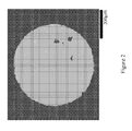
- FIG. 2 is a SEM image of a ⁇ 575 ⁇ m span of free-standing, single-layer graphene supported on etched Cu foil.
- FIG. 3 is a SEM image of an array of ⁇ 100 ⁇ m circular spans of free-standing, single-layer graphene supported on etched Cu foil.
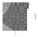
- FIG. 4 is a SEM image of a span of clean, free-standing, single-layer graphene prepared with ultra-pure ( ⁇ 99.999%) Cu foil.
- FIG. 5 is a higher magnification view (view corresponding to dotted box 401 in FIG. 4 ) showing removal of residual polymer by electron beam exposure around a small particle adhered to the graphene. This one defect present was intentionally imaged to confirm the presence of graphene.
- a photomask is used to pattern the photoresist and expose graphene 102B within the patterned regions.
- the patterned photoresist and exposed graphene 102B is then treated with O 2 plasma, thereby removing graphene 102B from the exposed areas.
- a first etch solution such as an isotropic etch solution (e.g. , 500 mM FeCl 3 iron(III) chloride), is used to wet etch the metal (i.e ., copper) in the exposed, patterned regions of the metal foil 101.
- the etch time is controlled and the first etching process is stopped before reaching the opposite side of the metal foil 101 and the graphene 102A.
- the etched distance of this first etching process is more than half-way ( i.e ., the distance etched during the first etching process is more than the total distance etched to reach the opposite side of the metal foil 101 and the graphene 102A). More generally, the etched distance of this first etching process is 90% of the distance to be etched to reach the opposite side of the metal foil 101 and the graphene 102A.
- the metal foil 101 can then be rinsed thoroughly with DI water to remove residual material left from the isotropic etchant.
- a second etchant solution having a more gentle effect e.g ., 50 mM (NH 4 ) 2 S 2 O 8 ammonium persulfate) is used to complete the etching of the metal foil 101 (copper) until the metal is completely removed from the surface of graphene 102A within the photoresist pattern.
- An etchant solution is "more gentle" than another etchant solution when it is less chemically reactive with regard to the material to be etched.
- the metal foil 101 can then be rinsed thoroughly with DI water to remove residuals left from the second etchant.
- the metal foil 101 is carefully rinsed with one or more solvents (such as acetone followed by isopropanol) to remove both the supporting photoresist layer 103 that was covering graphene 102A and the non-patterned photoresist 103 that was covering graphene 102B.
- solvents such as acetone followed by isopropanol
- the second etchant solution is preferably an anisotropic etchant solution, which is a reason why ammonium persulphate is a good etchant to use in the second etchant solution.
- Using ammonium persulphate also results in a more gentle etch during the second etchant step (as compared to the etch performed during the first etchant step using iron(III) chloride). Because ammonium persulphate will produce a more gentle etch (in comparison), this will generally require a higher standard of finish and possibly warming and will generally yield a slower etch rate for this latter etching step.
- the second etchant step can be isotropic, but this requires additional steps of patterning and etching to obtain the desired profile. When doing so the first etching process is performed for a majority of the way through the metal foil 101.
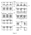
- FIGS. 6A-6J depict a scheme (Scheme 2) for patterning a material (e.g., another metal such as Au) in a controlled fashion on the suspended graphene window on a supported metal foil. Fabrication proceeds just as in Scheme No. 1, with the additional step of patterning and depositing the material on one side of the graphene-modified foil and then doing an aligned etch of the metal away from beneath the patterned feature.
- a material e.g., another metal such as Au
- graphene graphene 601A and graphene 601B
- graphene 601A and graphene 601B is grown ( e.g ., via CVD) on both sides of clean, pre-annealed metal foil 602 ( e.g ., Cu).
- photoresist 603 is spin-coated on both sides of the graphene-modified foil and photolithographically is used to define a deposition region 604.
- material 605 e.g., polymer, metal
- material 605 is deposited onto the patterned region 604 (e.g ., via electroplating or chemical bonding) or deposited uniformly onto the entire surface (e.g. , thermal or E-beam evaporation).
- a lift-off process is performed to define the patterned feature 606.
- protective polymer 607 e.g ., photoresist
- a process is performed to align and photolithographically pattern photoresist 608 on the backside of the graphene-modified foil.
- an etching process (dry or wet) is utilized to etch away graphene 601B in exposed region 609 of the polymer.
- the metal foil 602 is etched 610 through the patterned photoresist until the opposite graphene surface 611 of the graphene 601A is reached.
- the photoresist is dissolved and polymer residue is rinsed, which leaves behind suspended graphene window 612 with patterned material feature 606 atop it.
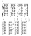
- FIGS. 7A-7H depict a scheme (Scheme 3) for creating graphene windows supported on metal foil having native or doped impurities, either intentionally doped or native to the foil, that exploits the tendency of the impurities to migrate to grain boundaries upon heating (during pre-annealing or during graphene growth) (i.e., the native or doped impurities concentrate at grain boundaries within the foil).
- Scheme 3 Scheme 3 for creating graphene windows supported on metal foil having native or doped impurities, either intentionally doped or native to the foil, that exploits the tendency of the impurities to migrate to grain boundaries upon heating (during pre-annealing or during graphene growth) (i.e., the native or doped impurities concentrate at grain boundaries within the foil).
- metal foil 701 e.g ., Cu
- native or doped impurities 702 is utilized.
- Grain boundaries 703 are indicated by dashed lines.
- impurities 702 move toward, and concentrate at, grain boundaries 703. As this occurs, the grain size increases (i.e., grain boundary density decreases).
- graphene graphene 704A and graphene 704B
- graphene 704A and graphene 704B is grown (e.g., via CVD) on both foil surfaces (which can result in additional migration and concentration of impurities).
- photoresist 705 is spin-coated on both sides of the graphene-modified foil.
- photolithographically is used to pattern resist 706 to allow exposed region 707 of the graphene to be etched away.
- an etching process (wet etch) is utilized to etch away metal foil 708 through the photoresist pattern 706.
- FIG. 7E an etching process
- the etching selectively stops at graphene-foil interface 709, leaving behind the intact graphene at this interface supported by photoresist with adhered, concentrated impurities 710 on the graphene 704A at the grain boundaries of the metal growth substrate.
- the photoresist is dissolved and polymer residue is rinsed, which leaves behind suspended graphene window 711 with adhered impurities 710 patterned along grain boundaries, creating nanoscale features.
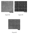
- FIGS. 8A-8C are SEM images of nanoscale impurities remaining after completing the fabrication of free-standing, single-layer graphene spans made using the scheme depicted in FIGS. 7A-7H .
- metal foils having ⁇ 99.8% Cu were utilized. It was found that impurities migrated towards the grain boundaries in the metal foil at elevated temperatures.
- FIGS. 9A-9I depict a scheme (Scheme 4) for creating a suspended graphene window on a metal foil (e.g., Cu) support that includes an isolated metal feature on the graphene window, i.e., in the center of the suspended graphene window the substrate is patterned, such as in an annular fashion.
- a metal foil e.g., Cu
- high purity, clean metal foil 901 e.g ., Cu
- metal foil 901 e.g ., Cu
- graphene graphene 902A and graphene 902B
- resolvable, photolithographically amenable polymer 903 i.e ., photoresist
- photolithography is used to pattern photoresist 904.
- FIG. 9E an etching process (dry or wet) is utilized to etch away graphene in exposed regions 905 of the photoresist.
- FIG. 9F the metal foil is etched 906 through photoresist.
- the etching process etches the metal foil down until opposite graphene surface 907 is reached, leaving behind an isolated Cu feature 908 adhered to the graphene 902A, as the graphene with photoresist island is under-etched away.
- FIG. 9H the photoresist is dissolved and polymer residue is rinsed, leaving behind the suspended graphene window 909 with adherent Cu feature 908.
- FIG. 9I is a top view of an isolated Cu feature 908 adhered to the graphene window 909 in the center of CVD grown graphene 902A on the Cu foil support.
- the center feature size By adjusting the center feature size relative to the foil thickness and etch time, the lateral and vertical dimensions of the isolated feature can be tuned.
- An isolated feature with an identical height as the foil thickness could be created by proper choice of dimension and abbreviated etch time (so as to prevent undercutting and release during etching).
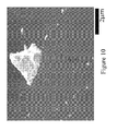
- FIG. 10 is an SEM image of an isolated Cu island formed on a suspended graphene structure made using the scheme depicted in FIGS. 9A-9I .
- the graphene was grown on lower-purity foil, so remaining impurities were seen adhered to the graphene.
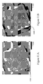
- FIGS. 11A-11B are SEM images of such an array of individualized mechanically-isolated metal foil supports. Sparse defects (tears, indicted with white arrows 1101 ) in the graphene can be seen in each image. By etching individually addressable regions of free-standing graphene windows, each region could be removed from the foil (as shown in FIGS. 12A-12B ) without mechanically damaging neighboring graphene features (processes like cutting can damage graphene structures).
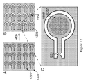
- photoresist features 1201 are patterned onto a graphene-modified metal foil 1202 (using the same or similar protocols described in abovementioned Schemes 1-4).
- FIG. 12B by etching through the exposed metal foil regions 1203, individualized arrays of free-standing graphene 1204 and 1207 can be produced.
- other features can be etched into each metal support structure to, for example, (i) aid in removal of each region from the array using perforations or narrowed sections 1205 or (ii) alignment of the region to a chip structure using alignment marks 1206.
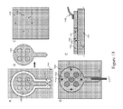
- metal foil 1301 has isolated and individualized Cu support containing an array of free-standing graphene features 1302 with etched alignment marks 1303.
- the individual Cu support 1305 is partitioned from the main sheet of foil (at 1304 of FIG 13A ).
- metal oxide chip 1306 features 1307 that spatially correspond to graphene features 1302 (shown on FIG. 13A ) on the foil array can be mated to the graphene array using alignment marks (1303 on FIG. 13C ) on the metal oxide chip.
- the individual Cu support 1305 can be secured and wire bonded 1308.
- alignment marks (1206 and 1303) can be etched into each Cu support to facilitate "pick-and-place” manufacturing (i.e ., each array can be aligned and placed onto a supporting chip structure with alignment marks (1310 in FIG. 13C ) so that the graphene features overlap specific regions of the chip that then integrate the graphene into the chip's functionality).
- the metal support e.g. , Cu
- this type of approach is useful for manufacturing arrays of graphene-based transmission electron microscopy (TEM) grids that are primarily used in research for sample analysis.
- TEM transmission electron microscopy
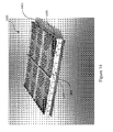
- FIG. 14 illustrates a high current graphene switch 1401 that uses a graphene window assembly 1402 that is mated with an insulator-conductor assembly 1403.
- FIG. 14 shows the alignment of the graphene windows 1404 with a group of etched features 1405 in the insulator-conductor assembly 1403.
- FIG. 15 is an SEM of a high current graphene switch.
- FIG. 15 shows the etched copper foil 1501 and the graphene 1502 in contact with etched features in the insulator-conductor assembly 1503.
- FIG. 15 shows the graphene wrinkles and tears at the edge of the graphene window 1504 when these windows overlap with the etched features in the insulator-conductor assembly 1503. This is a reason why it is beneficial to align these two assemblies before bringing them together (i.e., to avoid such wrinkling/tearing).
Landscapes
- Chemical & Material Sciences (AREA)
- Organic Chemistry (AREA)
- Engineering & Computer Science (AREA)
- Materials Engineering (AREA)
- Nanotechnology (AREA)
- Inorganic Chemistry (AREA)
- Carbon And Carbon Compounds (AREA)
Applications Claiming Priority (1)
| Application Number | Priority Date | Filing Date | Title |
|---|---|---|---|
| US14/039,707 US20140021165A1 (en) | 2010-12-23 | 2013-09-27 | Graphene windows, methods for making same, and devices containing same |
Publications (1)
| Publication Number | Publication Date |
|---|---|
| EP2853513A1 true EP2853513A1 (fr) | 2015-04-01 |
Family
ID=49885075
Family Applications (1)
| Application Number | Title | Priority Date | Filing Date |
|---|---|---|---|
| EP13199692.8A Withdrawn EP2853513A1 (fr) | 2013-09-27 | 2013-12-27 | Fenêtres de graphène, leurs procédés de fabrication et dispositifs les contenant |
Country Status (1)
| Country | Link |
|---|---|
| EP (1) | EP2853513A1 (fr) |
Cited By (1)
| Publication number | Priority date | Publication date | Assignee | Title |
|---|---|---|---|---|
| CN105399049A (zh) * | 2015-12-03 | 2016-03-16 | 中山大学 | 一种二维原子材料的微纳结构及图形化制备方法 |
Citations (2)
| Publication number | Priority date | Publication date | Assignee | Title |
|---|---|---|---|---|
| WO2012088274A1 (fr) * | 2010-12-23 | 2012-06-28 | Clean Energy Labs, Llc | Fenêtres en graphène, leurs procédés de fabrication et dispositifs les contenant |
| US20120258311A1 (en) * | 2009-10-16 | 2012-10-11 | Research & Business Foundation Sungkyunkwan University | Roll-to-roll transfer method of graphene, graphene roll produced by the method, and roll-to-roll transfer equipment for graphene |
-
2013
- 2013-12-27 EP EP13199692.8A patent/EP2853513A1/fr not_active Withdrawn
Patent Citations (2)
| Publication number | Priority date | Publication date | Assignee | Title |
|---|---|---|---|---|
| US20120258311A1 (en) * | 2009-10-16 | 2012-10-11 | Research & Business Foundation Sungkyunkwan University | Roll-to-roll transfer method of graphene, graphene roll produced by the method, and roll-to-roll transfer equipment for graphene |
| WO2012088274A1 (fr) * | 2010-12-23 | 2012-06-28 | Clean Energy Labs, Llc | Fenêtres en graphène, leurs procédés de fabrication et dispositifs les contenant |
Non-Patent Citations (3)
| Title |
|---|
| BENJAMÍN ALEMÁN ET AL: "Transfer-Free Batch Fabrication of Large-Area Suspended Graphene Membranes", ACS NANO, vol. 4, no. 8, 24 August 2010 (2010-08-24), pages 4762 - 4768, XP055038656, ISSN: 1936-0851, DOI: 10.1021/nn100459u * |
| JINGWEI BAI ET AL: "Graphene nanomesh", NATURE NANOTECHNOLOGY, NATURE PUBLISHING GROUP, LONDON, GB, vol. 5, 1 March 2010 (2010-03-01), pages 190 - 194, XP002698184, ISSN: 1748-3387, [retrieved on 20100214], DOI: 10.1038/NNANO.2010.8 * |
| XIAOGAN LIANG ET AL: "Formation of Bandgap and Subbands in Graphene Nanomeshes with Sub-10 nm Ribbon Width Fabricated via Nanoimprint Lithography", NANO LETTERS, vol. 10, no. 7, 14 July 2010 (2010-07-14), pages 2454 - 2460, XP055164436, ISSN: 1530-6984, DOI: 10.1021/nl100750v * |
Cited By (2)
| Publication number | Priority date | Publication date | Assignee | Title |
|---|---|---|---|---|
| CN105399049A (zh) * | 2015-12-03 | 2016-03-16 | 中山大学 | 一种二维原子材料的微纳结构及图形化制备方法 |
| CN105399049B (zh) * | 2015-12-03 | 2017-05-03 | 中山大学 | 一种二维原子材料的微纳结构及图形化制备方法 |
Similar Documents
| Publication | Publication Date | Title |
|---|---|---|
| EP2655246B1 (fr) | Procédés de fabrication de fenêtres en graphène | |
| CN102060292B (zh) | 制造和转移大尺寸石墨烯的方法 | |
| EP3367423B1 (fr) | Procédé d'obtention de graphène multicouche | |
| CN103682176B (zh) | 刚性衬底基板及柔性显示器件的制作方法、刚性衬底基板 | |
| US8080481B2 (en) | Method of manufacturing a nanowire device | |
| US20120107562A1 (en) | Methods for graphene-assisted fabrication of micro-and nanoscale structures and devices featuring the same | |
| JP6433430B2 (ja) | 三次元高表面領域電極の製造 | |
| JP2016537292A (ja) | シリコンカーバイド上のグラフェン層の形成方法 | |
| CN114361021B (zh) | 一种二维材料异质结器件及其制备方法 | |
| CN1935632A (zh) | 制造纳米线器件的方法 | |
| CN110061715B (zh) | 一种在非硅基底上制造压电薄膜谐振器的方法 | |
| JP2015187974A (ja) | 試料支持膜の製造方法 | |
| CN101499406B (zh) | 一种在绝缘衬底上制作硅化物纳米结构的方法 | |
| WO2012064177A1 (fr) | Membrane nanoporeuse et procédé de formation de celle-ci | |
| JP2006509229A (ja) | ディスプレイの製造方法 | |
| EP2853513A1 (fr) | Fenêtres de graphène, leurs procédés de fabrication et dispositifs les contenant | |
| KR101264877B1 (ko) | 실리콘 와이어 구조체의 제조방법 | |
| JP6713068B2 (ja) | カーボンナノチューブ複合膜で二次元ナノ材料を転写する方法 | |
| CN111320164A (zh) | 一种悬空石墨烯结构的制备方法及由其得到的悬空石墨烯结构和应用 | |
| WO2012125898A1 (fr) | Structures à base de graphène formant un motif sur du carbure de silicium | |
| US20140021165A1 (en) | Graphene windows, methods for making same, and devices containing same | |
| CN105460887B (zh) | 图形化多孔硅的制备方法 | |
| JP3950628B2 (ja) | 広範囲メンブランマスクを製造する方法 | |
| CN101559915A (zh) | 一种制备mems器件的牺牲层工艺方法 | |
| CN108840329B (zh) | 一种独立自支撑石墨烯基超薄膜的制备方法 |
Legal Events
| Date | Code | Title | Description |
|---|---|---|---|
| PUAI | Public reference made under article 153(3) epc to a published international application that has entered the european phase |
Free format text: ORIGINAL CODE: 0009012 |
|
| 17P | Request for examination filed |
Effective date: 20131227 |
|
| AK | Designated contracting states |
Kind code of ref document: A1 Designated state(s): AL AT BE BG CH CY CZ DE DK EE ES FI FR GB GR HR HU IE IS IT LI LT LU LV MC MK MT NL NO PL PT RO RS SE SI SK SM TR |
|
| AX | Request for extension of the european patent |
Extension state: BA ME |
|
| STAA | Information on the status of an ep patent application or granted ep patent |
Free format text: STATUS: THE APPLICATION IS DEEMED TO BE WITHDRAWN |
|
| 18D | Application deemed to be withdrawn |
Effective date: 20151002 |