EP2856636B1 - Amplificateur de puissance rf basé sur un transformateur - Google Patents
Amplificateur de puissance rf basé sur un transformateur Download PDFInfo
- Publication number
- EP2856636B1 EP2856636B1 EP12877964.2A EP12877964A EP2856636B1 EP 2856636 B1 EP2856636 B1 EP 2856636B1 EP 12877964 A EP12877964 A EP 12877964A EP 2856636 B1 EP2856636 B1 EP 2856636B1
- Authority
- EP
- European Patent Office
- Prior art keywords
- power amplifier
- conductive
- cells
- conductive contacts
- coupled
- Prior art date
- Legal status (The legal status is an assumption and is not a legal conclusion. Google has not performed a legal analysis and makes no representation as to the accuracy of the status listed.)
- Active
Links
Images




Classifications
-
- H—ELECTRICITY
- H03—ELECTRONIC CIRCUITRY
- H03F—AMPLIFIERS
- H03F3/00—Amplifiers with only discharge tubes or only semiconductor devices as amplifying elements
- H03F3/20—Power amplifiers, e.g. Class B amplifiers, Class C amplifiers
- H03F3/21—Power amplifiers, e.g. Class B amplifiers, Class C amplifiers with semiconductor devices only
- H03F3/213—Power amplifiers, e.g. Class B amplifiers, Class C amplifiers with semiconductor devices only in integrated circuits
-
- H—ELECTRICITY
- H03—ELECTRONIC CIRCUITRY
- H03F—AMPLIFIERS
- H03F3/00—Amplifiers with only discharge tubes or only semiconductor devices as amplifying elements
- H03F3/189—High-frequency amplifiers, e.g. radio frequency amplifiers
- H03F3/19—High-frequency amplifiers, e.g. radio frequency amplifiers with semiconductor devices only
- H03F3/195—High-frequency amplifiers, e.g. radio frequency amplifiers with semiconductor devices only in integrated circuits
-
- H—ELECTRICITY
- H03—ELECTRONIC CIRCUITRY
- H03F—AMPLIFIERS
- H03F3/00—Amplifiers with only discharge tubes or only semiconductor devices as amplifying elements
- H03F3/20—Power amplifiers, e.g. Class B amplifiers, Class C amplifiers
- H03F3/21—Power amplifiers, e.g. Class B amplifiers, Class C amplifiers with semiconductor devices only
- H03F3/211—Power amplifiers, e.g. Class B amplifiers, Class C amplifiers with semiconductor devices only using a combination of several amplifiers
-
- H—ELECTRICITY
- H03—ELECTRONIC CIRCUITRY
- H03F—AMPLIFIERS
- H03F3/00—Amplifiers with only discharge tubes or only semiconductor devices as amplifying elements
- H03F3/20—Power amplifiers, e.g. Class B amplifiers, Class C amplifiers
- H03F3/24—Power amplifiers, e.g. Class B amplifiers, Class C amplifiers of transmitter output stages
-
- H—ELECTRICITY
- H03—ELECTRONIC CIRCUITRY
- H03F—AMPLIFIERS
- H03F3/00—Amplifiers with only discharge tubes or only semiconductor devices as amplifying elements
- H03F3/20—Power amplifiers, e.g. Class B amplifiers, Class C amplifiers
- H03F3/24—Power amplifiers, e.g. Class B amplifiers, Class C amplifiers of transmitter output stages
- H03F3/245—Power amplifiers, e.g. Class B amplifiers, Class C amplifiers of transmitter output stages with semiconductor devices only
-
- H—ELECTRICITY
- H03—ELECTRONIC CIRCUITRY
- H03F—AMPLIFIERS
- H03F3/00—Amplifiers with only discharge tubes or only semiconductor devices as amplifying elements
- H03F3/45—Differential amplifiers
- H03F3/45071—Differential amplifiers with semiconductor devices only
- H03F3/45076—Differential amplifiers with semiconductor devices only characterised by the way of implementation of the active amplifying circuit in the differential amplifier
- H03F3/45179—Differential amplifiers with semiconductor devices only characterised by the way of implementation of the active amplifying circuit in the differential amplifier using MOSFET transistors as the active amplifying circuit
-
- H—ELECTRICITY
- H04—ELECTRIC COMMUNICATION TECHNIQUE
- H04B—TRANSMISSION
- H04B1/00—Details of transmission systems, not covered by a single one of groups H04B3/00 - H04B13/00; Details of transmission systems not characterised by the medium used for transmission
- H04B1/02—Transmitters
- H04B1/04—Circuits
-
- H—ELECTRICITY
- H03—ELECTRONIC CIRCUITRY
- H03F—AMPLIFIERS
- H03F2200/00—Indexing scheme relating to amplifiers
- H03F2200/451—Indexing scheme relating to amplifiers the amplifier being a radio frequency amplifier
-
- H—ELECTRICITY
- H03—ELECTRONIC CIRCUITRY
- H03F—AMPLIFIERS
- H03F2200/00—Indexing scheme relating to amplifiers
- H03F2200/541—Transformer coupled at the output of an amplifier
-
- H—ELECTRICITY
- H03—ELECTRONIC CIRCUITRY
- H03F—AMPLIFIERS
- H03F2203/00—Indexing scheme relating to amplifiers with only discharge tubes or only semiconductor devices as amplifying elements covered by H03F3/00
- H03F2203/20—Indexing scheme relating to power amplifiers, e.g. Class B amplifiers, Class C amplifiers
- H03F2203/21—Indexing scheme relating to power amplifiers, e.g. Class B amplifiers, Class C amplifiers with semiconductor devices only
- H03F2203/211—Indexing scheme relating to power amplifiers, e.g. Class B amplifiers, Class C amplifiers with semiconductor devices only using a combination of several amplifiers
- H03F2203/21142—Output signals of a plurality of power amplifiers are parallel combined to a common output
-
- H—ELECTRICITY
- H03—ELECTRONIC CIRCUITRY
- H03F—AMPLIFIERS
- H03F2203/00—Indexing scheme relating to amplifiers with only discharge tubes or only semiconductor devices as amplifying elements covered by H03F3/00
- H03F2203/45—Indexing scheme relating to differential amplifiers
- H03F2203/45394—Indexing scheme relating to differential amplifiers the AAC of the dif amp comprising FETs whose sources are not coupled, i.e. the AAC being a pseudo-differential amplifier
-
- H—ELECTRICITY
- H03—ELECTRONIC CIRCUITRY
- H03F—AMPLIFIERS
- H03F2203/00—Indexing scheme relating to amplifiers with only discharge tubes or only semiconductor devices as amplifying elements covered by H03F3/00
- H03F2203/45—Indexing scheme relating to differential amplifiers
- H03F2203/45682—Indexing scheme relating to differential amplifiers the LC comprising one or more op-amps
-
- H—ELECTRICITY
- H03—ELECTRONIC CIRCUITRY
- H03F—AMPLIFIERS
- H03F2203/00—Indexing scheme relating to amplifiers with only discharge tubes or only semiconductor devices as amplifying elements covered by H03F3/00
- H03F2203/45—Indexing scheme relating to differential amplifiers
- H03F2203/45731—Indexing scheme relating to differential amplifiers the LC comprising a transformer
-
- H—ELECTRICITY
- H04—ELECTRIC COMMUNICATION TECHNIQUE
- H04B—TRANSMISSION
- H04B1/00—Details of transmission systems, not covered by a single one of groups H04B3/00 - H04B13/00; Details of transmission systems not characterised by the medium used for transmission
- H04B1/02—Transmitters
- H04B1/04—Circuits
- H04B2001/0408—Circuits with power amplifiers
Definitions
- Embodiments described herein relate to transformers and power amplifiers. Some embodiments relate to radio frequency (RF) power amplifiers in semiconductor devices.
- RF radio frequency
- power amplifiers and transformers to boost a power level of a signal for various applications.
- the power amplifier, the transformer, or both may need to be in a certain configuration.
- the size of the power amplifier, transformer, or both may relatively large.
- heat generated by the power amplifier may become a factor; connections between the power amplifier and the transformer may be hard to arrange; and supply power may be difficult to be routed to the power amplifier. Therefore, in such cases, designing power amplifiers to suit some applications may pose a challenge.
- HONGTAO XU ET AL "A Flip-Chip-Packaged 25.3 dBm Class-D Outphasing Power Amplifier in 32 nm CMOS for WLAN Application", IEEE JOURNAL OF SOLID-STATE CIRCUITS, IEEE SERVICE CENTER, PISCATAWAY, NJ, USA, (20110701), vol. 46, no. 7, doi:10.1109/JSSC.2011.2143930, ISSN 0018-9200, PAGE 1596 - 1605 , discloses a power amplifier with a nMOS cascode transistor layout in which V d and V s are collected by horizontal metal strips routed on top of the device and drain-source contacts are shared between adjacent cascode devices. Moreover, a power combiner is designed with a transmission line transformer.
- ICHIRO AOKI ET AL "A Fully-Integrated Quad-Band GSM/GPRS CMOS Power Amplifier", IEEE JOURNAL OF SOLID-STATE CIRCUITS, IEEE SERVICE CENTER, PISCATAWAY, NJ, USA, (20081201), vol. 43, no. 12, doi:10.1109/JSSC.2008.2004870, ISSN 0018-9200, PAGE 2747 - 2758 , discloses a power amplifier having a power control loop technology employing current mode routing. The power control loop operates under a voltage regulator whose output voltage is maintained constant under all supply conditions.
- FIG. 1 shows a schematic diagram of a device 100 including power amplifier 101 having power amplifier cells 111 through 126 and a combiner 130, according to some embodiments described herein.
- Device 100 may include or be included in wireless communication devices (e.g., cellular phones such as smart phones), computers (e.g., tablet computers), and other electronic devices or systems.
- wireless communication devices e.g., cellular phones such as smart phones
- computers e.g., tablet computers
- each of power amplifier cells 111 through 126 may include an input node to receive an input signal (e.g., signal labeled "+” or "-").
- the input signal may include a component of a differential signal (e.g., input differential signal).
- Each of power amplifier cells 111 through 126 may include an output node.
- the output nodes e.g., 111a, 112a, 113a, and 114a
- Each of power amplifier cells 111 through 126 may amplify the signal (signals "+” and "-”) at its respective input node and provide amplified signal at its output node.
- FIG. 1 shows power amplifier 101 including eight differential pairs as an example. The number of differential pairs may vary.
- the output node of each power amplifier cells 111 through 126 may provide an output signal, which may include a component of a differential signal associated with a respective differential pair.
- Each of the power amplifier pairs (form by two of power cells 111 through 126) may amplify the signals (signals "+” and "-") at its respective input nodes and provide amplified signals at its output nodes.
- Combiner 130 of power amplifier 101 may include a transformer circuit (e.g., a transformer combining circuit) 140 having transformer sections 140a, 140b, 140c, and 140d. Each these four transformer sections may include two transformers.
- transformer circuit 140 may include eight transformers. The eight transformers may operate to combine (e.g., transform) signals from the output nodes of power amplifier cells 111 through 126 and provide output signals Vout+ and Vout- at the output nodes (shown in FIG. 1 as two circles next to signals Vout+ and Vout) of power amplifier 101.
- the Vout+ and Vout-signals may form components of a differential signal (e.g., output differential signal) provided by power amplifier 101.
- power amplifier 101 may include a transformer-based power amplifier having a 4-section 8-way transformer combiner configuration.
- combiner 130 may include conductive lines 131 through 138 and associated inductors L131 through L138, and a conductive line 139 and associated inductors 139a through 139d.
- Combiner 130 may include connections 151 through 158, each of which may be coupled between the output nodes of two power amplifier cells. In some cases, some or all of connections 151 through 158 may be omitted from combiner 130.
- Conductive lines 131 through 138 and inductors L131 through L138 may form part of a primary (e.g., primary windings) of transformer circuit 140.
- Conductive line 139 and inductors 139a through 139d may form part of a secondary (e.g., a second winding) of transformer circuit 140.
- Each of inductors L131 through L138 may be coupled between two output nodes of two respective power amplifier cells through one of conductive lines 131 through 138.
- inductor L131 may be coupled between the output nodes power amplifier cells 112 and 113 through conductive line 131.
- inductor L133 may be coupled between the output nodes power amplifier cells 114 and 119 through conductive line 133.
- the inductor (one of L131 through 138) coupled between two power amplifier cells may be located adjacent one of the inductors L139a through L139c to form part of a transformer at one of transformer section 140a, 140b, 140c, and 140d.
- inductor L131 and inductor L139a may form part of a transformer at transformer section 140a.
- inductor L132 and inductor L139a may form part of another transformer at transformer section 140a.
- Each of power amplifier cells 111 through 126 may include a single transistor or multiple transistors.
- FIG. 1 shows only four transistors T119, T120, T121, and T122 included in four respective power amplifier cells 119, 120, 121, and 114.
- Each of the other power amplifier cells may include a single transistor or multiple transistors similar to transistors T119, T120, T121, and T122.
- the transistors of power amplifier cells 111 through 126 may include field effect transistors, such as transistors fabricated using complementary metal-oxide-semiconductor (CMOS) processes.
- CMOS complementary metal-oxide-semiconductor
- power amplifier cells 111 through 126 may include CMOS transistors.
- power amplifier cells 111 through 126 may include n-channel MOS (NMOS) transistors and/or p-channel MOS (PMOS) transistors.
- Each of power amplifier cells 111, 112, 113, and 114 may receive either input signal (e.g., "+” or signal "-") at the gate its respective transistor.
- power amplifier cells 119, 120, 121, and 122 may receive their input signals at the gates of transistors (e.g., NMOS transistors) T119, T120, T121, and T122, respectively.
- the output signal of each of power amplifier cells 111, 112, 113, and 114 can be provided at the drain of their transistors, such as at the drain of transistors T119, T120, T121, and T122.
- Each of power amplifier cells 111 through 126 may include supply nodes 198 and 199 to receive power and ground signals, respectively.
- supply nodes 198 and 199 of only two power amplifier cells 112 and 113 are shown in FIG. 1 .
- Power and ground signals may be provided (e.g., coupled) to the transistors of power amplifier cells 111 to 126 through supply nodes 198 and 199.
- the transistors (e.g., T119, T120, T121, and T122) of power amplifier 101 may operating at a supply voltage (e.g., provided at node 198) of approximately one volt.
- Power amplifier 101 may have an output power of in a range of approximately 26dBm to approximately 32dBm and a peak drain efficiency of approximately 50%.
- the output power of power amplifier 101 may be provided by the form of signals (e.g., Vout+ and Vout-) at its output nodes (nodes next to signals Vout+ and Vout- in FIG. 1 ).
- Device 100 may include or be included in a system in a chip (SoC), such that power amplifier 101 may be integrated such a system (e.g., form in the same die with other elements, such as a processing unit and a memory).
- SoC system in a chip
- Power amplifier 101 may be implemented such that it may be a compact, low-loss, high radio RF output power, transformer-based RF power amplifier, as described below with reference to FIG. 2A through FIG. 3C .
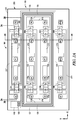
- FIG. 2A shows a top view of a structure of device 100 of FIG. 1 including a die 200, according to some embodiments described herein.
- Die 200 may include a semiconductor die (e.g., a silicon die) where at least a portion of power amplifier cells 113 through 126 and at least a portion of combiner 130 may be formed.
- a semiconductor die e.g., a silicon die
- Die 200 may include a surface 210 and conductive contacts G1 through G8 and P1 through P12 overlying surface 210. These conductive contacts may include solder bumps. Die 200 may be included in a flip-chip package, such that conductive contacts G1 through G8 and P1 through P12 may be coupled to a package substrate (not shown in FIG. 2A ) of the flip-chip package without using wires (e.g., without bonding wires). For example, conductive contacts G1 through G8 and P1 through P12 may be coupled to a package substrate of a flip-chip package through controlled collapse chip connections (C4) or other types of connections.
- C4 controlled collapse chip connections
- Die 200 may include other conductive contacts similar to or identical to conductive contacts G1 through G8 and P1 through P12.
- the other conductive contacts may be used to carry signals such as data and clock signals.
- the other conductive contacts of die are not shown in FIG. 2A .
- conductive contacts G1 through G8 and P1 through P12 may be coupled to a supply source (e.g., a battery or an alternate current (AC) power source) to receive supply signals (e.g., power and ground signals).
- a supply source e.g., a battery or an alternate current (AC) power source
- supply signals e.g., power and ground signals
- some or all of conductive contacts P1 through P12 may receive power signals from the supply source.
- Some or all or conductive contacts G1 through G8 may receive ground signals from the supply source.
- some of the conductive contacts G1 through G8 and P1 through P12 may be configured to carry signals other than supply signals (e.g., data signals and/or clock signals).
- conductive contacts G1 through G8 and P1 through P12 may be arranged in rows and columns with respect to the X-direction and the Y-direction. Conductive contacts G1 through G8 may be electrically separated from conductive contacts P1 through P12. However, some of conductive contacts G1 through G8 may be coupled together, and some of conductive contacts P1 through P8 may be coupled together.
- FIG. 2A shows some of conductive contacts P1 through P12 may be coupled to each other through respective connections 211 through 215. Conductive contacts G3 and G5 may be coupled to each other through a connection 216.
- FIG. 2A also shows a connection 217 coupled to conductive contact G1 and a connection 218 coupled to conductive contact G7.
- Conductive contacts G1 through G8 may receive the same or similar signals (e.g., ground signals). Conductive contacts P1 through P12 may receive the same or similar signals (e.g., power signals) but may be different from the signals received by conductive contacts G1 through G8. Thus, as shown in FIG. 2A , conductive contacts G1 through G8 may form a group and may be located on one side (e.g., left side) of surface 210 of die 200. Conductive contacts P1 through P12 may form another group and may be located on another side (e.g., right side) of surface 210 of die 200.
- conductive lines 131 through 139 may be located in different areas of surface 210 between conductive contacts G1 through G8 and P1 through P12.
- Inductors L131 through L139 shown in FIG. 1 may be a transmission line type inductor, such that each inductor may be included in (in other words, may be part of) a respective conductive line among conductive lines 131 through 139.
- combiner 130 may include no separate (e.g., no additional) inductors besides conductive lines 131 through 139. Therefore, conductive lines 131 through 139 may assume the functions of respective inductors L131 through L139 ( FIG. 1 ).
- Each of conductive lines 131 through 139 may include a conductive material overlying surface 210 of die 200.
- the conductive material may include copper, gold, or other metals or alloys.
- Connections 211 through 218 (coupled to some of conductive contacts G1 through G8 and some of conductive contacts P1 through P8) may include conductive materials similar to or identical to the materials of conductive lines 131 through 139.
- Conductive lines 131 to 138 in FIG. 2A may correspond to the primary of the transformer circuit 140 ( FIG. 1 ).
- Conductive line 139 in FIG. 2A may correspond to the secondary of transformer circuit 140.
- each transformer in each of transformer sections 140a, 140b, 140c, and 140d may include a single turn (e.g., single primary and single secondary winding) transmission line transformer. Therefore, transformer circuit 140 may include a single turn transmission line type transformer circuit.
- conductive line 139 may forms at least part of a loop.
- the loop may include an inside that surrounds an area of surface 210 where conductive contacts G3 through G6 and P4 through P9 are located.
- the loop may include an outside corresponding to an area of surface 210 where conductive contacts G1, G2, G7, G8, P1, P2, P3, P10, P11, and P12 are located.
- Conductive line 139 may be coupled to other elements 149 of device 100.
- Conductive lines 131 through 138 may be located inside or outside the loop formed by conductive line 139.
- conductive lines 132, 134, 136, and 138 may be located inside the loop.
- Conductive lines 131, 133, 135, and 137 may be located outside the loop.
- Multiple conductive segments of conductive lines 131 through 139 may located between two of conductive contacts G1 through G8 and P1 through P12.
- three conductive segments of three respective conductive lines 131, 132, and 139 along the X-direction may be located between conductive contacts G2 and G4, P1 and P4, or P2 and P5.
- three conductive segments of three respective conductive lines 135, 136, and 139 along the X-direction may be located between conductive contacts G6 and G8, P7 and P10, or P8 and P11.
- power amplifier cells 111 through 126 may be formed in portions 201 through 208 in die 200 and below surface 210.
- FIG. 2B shows the same top view of the structure of the device 100 of FIG. 2A but without conductive lines 131 through 139.
- FIG. 2B also shows a die area (e.g., a square or a rectangle) 280 in die 200 where power amplifier cells 111 through 126 are located.
- power amplifier cells 111 through 126 may be distributed (e.g., in an equal number of amplifier cells) among the eight locations associated with portions 201 through 208 within die area 280 of die 200. Each of the eight locations may include two of power amplifier cells 111 through 126.
- a group of power amplifier cells may be located inside transformer circuit 140 (e.g., located in the loop formed by conductive line 139).
- Another group of power amplifier cells e.g., 111 through 114 and 119 through 122 may be located outside transformer circuit 140 (e.g., located outside the loop formed by conductive line 139).
- Conductive contacts G1 through G8 and P1 through P12 may be coupled to portions 201 through 208 (locations of power amplifier cells 111 through 126) through a number of routings.
- the routings may include a combination of connections (e.g., 211 through 218) overlying surface 210 and conductive paths ( FIG. 3A and FIG. 3B ) below surface 210 coupled to the connections.
- the conductive paths may extend between surface 210 and portions 201 through 208 in die 200.
- power amplifier cells 111 and 112 (at portion 201) and 113 and 114 (at portion 202) may be coupled to conductive contact G1 through connection 217 and to conductive contacts P1 and P2 through connection 211.
- Power amplifier cells 115 and 116 (at portion 203) and 117 and 118 (at portion 204) may be coupled to contracts G3 and G5 through connection 216 and to conductive contacts P4 and P5 through connection 212.
- Power amplifier cells 119 and 120 (at portion 205) and 121and 122 (at portion 206) may be coupled to contract G7 through a connection 217 and to conductive contacts P10 and P11 through connection 214.
- Power amplifier cells 123 and 124 (at portion 207) and 125 and 126 (at portion 208) may be coupled to contracts G3 and G5 through a connection 216 and to conductive contacts P7 and P8 through connection 213.
- the structure of power amplifier 101 may allow die 200 to be used efficiently, the size of power amplifier 101 to be compact, and heat distribution to be improved.
- some conventional transformers may occupy a relatively large area of a device because transformer components (e.g., inductors) usually require dedicated area away from other passive and active components of the device.
- transformer components e.g., inductors
- Conventional transformers in some types of IC packages e.g., flip chip package
- conductive contacts e.g., solder bumps
- device area e.g., area on surface 210
- the conductor turns (e.g., conductive lines 131 through 139) of the transformers of transformer circuit 140 may be routed in surface areas between conductive contacts G1 through G8 and P1 through P12.
- the topology described herein may also be fit into flip-chip packages and may still allow regular solder bump pattern (e.g., pattern including conductive contacts G1 through G8 and P1 through P12) of the flip-chip packages to maintain compliance with package design rules.
- the size of power amplifier 101 may be relatively smaller than that of some conventional power amplifiers.
- power cells 111 through 126 may be located inside and outside ( FIG. 2A ) transformer circuit 140, power cells 111 through 126 may occur a relatively compact area, which may be smaller than that of some conventional power amplifiers.
- die area 280 FIG. 2B ) may be approximately 0.8 square millimeters.
- power cells 111 through 126 of power amplifier 101 may be evenly distributed in various portions of die 200 within die area 280, heat from power amplifier 101 may uniformly spread, such as by dissipating through a body (e.g., well) of die 200. This may reduce hotspots in die 200 (or in an IC package that contains die 200).
- the structure of power amplifier 101 may allow it to be implemented using digital devices, such as a combination of NMOS and PMOS transistors.
- each of the multi-section transformers may need to have similar or identical inductance and coupling factor to obtain maximum performance.
- Some conventional power amplifiers may have amplifier cells with transistors gate rotate 90 degrees among each other to maintain symmetry.
- CMOS process may not be applicable to fabricate transistors in some conventional power amplifiers because the mentioned 90 degrees orientation would violate CMOS process rules.
- the arrangement of power amplifier cells 111 through 126 as shown in FIG. 2A may satisfy the inductance and coupling factor for multi-section transformers.
- the arrangement of power amplifier cells 111 through 126 may also avoid the 90 degree gate rotation that some conventional power amplifiers may require.
- the gates of transistors in power amplifier cells 111 through 126 may extend in the same direction (e.g., the X-direction or the Y-direction in FIG. 2A ). This may allow power amplifier 101 to comply with CMOS process design rules.
- transistors of power amplifier 101 may be structured using CMOS.
- the transformers (e.g., at sections 140a through 140d) of power amplifier may be located close to each other, thereby the size of power amplifier 101 may be further reduced.
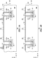
- FIG. 3A shows a cross section along the X-direction of device 100 of FIG. 2A including connections 211 and 217 overlying surface 210 of die 200 and conductive paths 311a, 311b, 318a, and 318b formed in portion 341 of die 200.
- Portion 341 may include one or more layers having routings (metallization routings) to carry signals internally among components of die 200 or signals between components of die 200 and other external devices.
- conductive paths 311a, 311b, 318a, and 318b may extend between surface 210 and portions 201 through 208 in die 200.
- Each of conductive paths 311a, 311b, 318a, and 318b may be formed in one or more via (e.g., holes containing conductive material) in portion 341.
- FIG. 3A shows an example where each of conductive paths 311a, 311b, 318a, and 318b may completely extend vertically along the Z-direction, which is substantially perpendicular to the X-direction.
- Each of conductive paths 311a, 311b, 318a, and 318b may include one or more segment that may extend in a different direction different from the Z-direction (e.g., extend horizontally along the X-direction or the Y-direction).
- Connections 151 through 158 may be formed in portion 341. As described above, some or all of connections 151 through 158 may be omitted.
- conductive contacts P1 and P2 may be coupled to supply node 198 associated with power amplifier cell 112 through connection 211 and conductive path 311a. Conductive contacts P1 and P2 may also be coupled to supply node 198 associated with power amplifier cell 113 through connection 211 and conductive path 311b. Power amplifier cells 111 and 112 may share the same connection at supply node 198 at portion 201. Power amplifier cells 113 and 114 may share the same connection at supply node 198 at portion 201.
- Conductive contact G1 may be coupled to supply node 199 associated with power amplifier cell 112 through connection 217 and conductive path 318a. Conductive contact G1 may also be coupled to supply node 199 associated with power amplifier cell 113 through connection 217 and conductive path 318b. Power amplifier cells 111 and 112 may share the same connection at supply node 199 at portion 201. Power amplifier cells 113 and 114 may share the same connection at supply node 199 at portion 202.
- Certain types of IC packages may have power contacts grouped in one side of a surface of the device and ground contacts grouped in another side of the surface of the device. This may limit power and ground signals to be delivered to some other areas of the device.
- using conductive lines 211 through 218 ( FIG. 2A ) and conductive paths 311a, 311b, 318a, and 381b ( FIG. 3A to directly couple conductive contacts G1 through G8 and P1 through P12 to supply nodes (e.g., 198 and 199 in FIG. 3A of the power amplifier cells may provide robust un-interrupted and dedicated connections from conductive contacts G1 through G8 and P1 through P12 to the power amplifier cells to the power amplifier cells. This may provide a robust and un-interrupted supply network (e.g., power and ground signals) from conductive contacts G1 through G8 and P1 through P12 to the power amplifier cells.
- FIG. 3B shows another cross section along the X-direction of device 100 of FIG. 2A including conductive lines 131, 133, and 137 overlying surface 210 of die 200 and conductive paths 331a, 331b, 333, and 337 formed in portion 341 of die 200.
- conductive paths 331a, 331b, 333, and 337 may extend between surface 210 and portions 201 through 208 in die 200.
- Each of conductive paths 331a, 331b, 333, and 337 may be formed in one or more via (e.g., holes containing conductive material) in portion 341.
- each of conductive paths 311a, 331a, 331b, 333, and 337 may completely extend vertically along the Z-direction.
- Each of conductive paths 331a, 331b, 333, and 337 may include one or more segment that may extend in a different direction different from the Z-direction (e.g., extend horizontally along the X-direction or the Y-direction).
- conductive line 131 may be coupled to output nodes 112a and 113a of power amplifier cells 112 and 113, respectively, through conductive paths 331a and 331b.
- Conductive line 133 may be coupled to output node 114a of power amplifier cell 114 through conductive path 333.
- Conductive line 137 may be coupled to output node 111a of power amplifier cell 111 through conductive path 337.
- each of power amplifier cells 111 through 126 may include a single transistor or multiple transistors.
- each of power amplifier cells 111 through 124 may include one or more transistors that can be formed in portions 201 and 202.
- the transistors may be formed using CMOS processes.
- the gates of the transistors may extend in the same direction (e.g., the X-direction or the Y-direction).
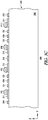
- FIG. 3C shows a cross section along the Y-direction of device 100 of FIG. 2A .
- three conductive segments of three respective conductive lines 131, 132, and 139 may be located between conductive contact P2 and P5.
- Three conductive segments of three respective conductive lines 135, 136, and 139 may be located between conductive contacts P8 and P11.
- power amplifier 101 may include power amplifier cells 111 through 126 formed in die 200 ( FIG. 2A ), at least part of conductive contacts G1 through G8 and P1 through P12 overlying surface 210 of die 200, and conductive lines 131 through 139 overlying surface 210.
- Power amplifier 101 may include connections (e.g., 211 through 219 in FIG. 2A ) overlying surface 210 and coupled to some of conductive contacts G1 through G8 and P1 through P12.
- Power amplifier 101 may include conductive paths (e.g., 311a, 311b, 318a, 318b, 331a, 331b, 333, and 337 in FIG. 3A and FIG.
- Power amplifier cells 111 through 126 may include supply nodes (e.g., 198 and 199 in FIG. 3A and FIG. 3B ) coupled to some of the conductive contacts G1 through G8 and P1 through P12 through the connections and the conductive paths.
- supply nodes e.g., 198 and 199 in FIG. 3A and FIG. 3B
- FIG. 4 shows a block diagram of user equipment 400 including an interface 410 according to some embodiments described herein.
- User equipment may include device 100 described above with reference to FIG. 1 through FIG. 3C .
- user equipment may also include antennas 413 and 414, a processing unit 431, and a memory 441.
- FIG. 4 omits other elements of device 100 to not obscure the embodiments described herein.
- device 100 may include one or more of a keyboard, a display (e.g., an LCD screen including a touch screen), a non-volatile memory port (e.g., a Universal Serial Bus (USB) port), a graphics processor, an application processor, speakers, and other elements.
- a keyboard e.g., an LCD screen including a touch screen
- a non-volatile memory port e.g., a Universal Serial Bus (USB) port
- graphics processor e.g., an application processor, speakers, and other elements.
- User equipment 400 may include portable wireless communication device, such as a personal digital assistant (PDA), a laptop or portable computer with wireless communication capability, a web tablet, a wireless telephone, a wireless headset, a pager, an instant messaging device, a digital camera, an access point, a television, a medical device (e.g., a heart rate monitor, a blood pressure monitor, etc.), or other device that may receive and/or transmit information wirelessly.
- PDA personal digital assistant
- laptop or portable computer with wireless communication capability such as a personal digital assistant (PDA), a laptop or portable computer with wireless communication capability, a web tablet, a wireless telephone, a wireless headset, a pager, an instant messaging device, a digital camera, an access point, a television, a medical device (e.g., a heart rate monitor, a blood pressure monitor, etc.), or other device that may receive and/or transmit information wirelessly.
- Processing unit 431 and interface 410 of user equipment 400 may be configured to communicate with a single type of communication network or multiple types of communication networks.
- processing unit 431 and interface 410 may be configured to communicate with one or more of WiFi, WiMax, LTE, and other communication networks.
- Processing unit 431 may include a single processor or multiple processors.
- the processor or processors may include one or more general purpose processors, one or more application-specific integrated circuits (ASICs), or other types of processors.
- Processing unit 431 may configure messages for transmission by interface 410 to other devices.
- Processing unit 431 may be configured to communicate with the interface 410 to wirelessly exchange messages with other devices.
- Memory 441 may include volatile memory, non-volatile memory, or a combination of both.
- Memory 441 may contain instructions (e.g., firmware programs, software programs, or a combination of both), which when executed by processing unit 431 result in user equipment performing operations. Such operations may include wirelessly transmitting, receiving, or both, signals to or from user equipment through antennas 413 and 414.
- interface 410 may include transceivers 411 and 412, each of which may be configured to communicate with a different network.
- transceiver 411 may be configured to communicate with an LTE network
- transceiver 412 may be configured to communicate with a WiMax network.
- FIG. 4 shows an example where user equipment includes two transceivers (e.g., 421 and 422) and two antennas (e.g., 413 and 414). The number of transceivers and antennas may vary.
- Transceiver 411 may include a transmitter 421 and a receiver 422 to wirelessly exchange (e.g., send and receive) messages with other devices (not shown in FIG. 4 ) through at least one of antennas 413 and 414 in at least one of the networks described above.
- Transceiver 412 may also include a transmitter and a receiver (not shown in FIG. 4 ) to wirelessly exchange messages with other devices through at least one of antennas 413 and 414.
- Device 100 may include or be included in user equipment (e.g., a cellular phone, a tablet computer, or other equipments).
- user equipment e.g., a cellular phone, a tablet computer, or other equipments.
- the transmitter 421 may be part of user equipment configured to operate in an LTE network or in another single network or multiple networks among the networks described above (e.g., WiFi, WiMax, and other networks).
- At least one of transceivers 411 and 412 may include a power amplifier.
- transmitter 412 of transceiver 411 may include power amplifier 401.
- Power amplifier 401 may include power amplifier 101 described above with reference to FIG. 1 through FIG. 3C .
- transmitter 412 may include circuitry 402 to generate signals for transmission.
- Power amplifier 401 may receive signals (e.g., input signals) generate by circuitry 402 and provide signals (e.g., output signals) to at least one of antennas 413 and 414 for transmission.
- the signals (e.g., input signals) received by power amplifier 401 may include signals similar to or identical to signals "+" and "-" received by power amplifier 101 described above with reference to FIG. 1 through FIG. 3C .
- the signals (e.g., output signals) provided by power amplifier 401 to antennas 413 and 414 may include signals similar to or identical to signals Vout+ and Vout- (or alternatively, signals based on signals Vout+ and Vout-) provided by power amplifier 101.
- Transmitter 421 of transceiver 411 in FIG. 4 may include an OFDM transmitter, such that at least one of the signals generated by circuitry 402 may include an orthogonal frequency-division multiplexing (OFDM) signal.
- User equipment 400 may be configured to operate in a multiple-input multiple-output (MIMO) configuration.
- power amplifier 401 may be coupled to multiple antennas of user equipment 400 (e.g., at least antennas 413 and 414) for MIMO transmissions.
- the signals generated by circuitry 402 may include precoded OFDM signals for MIMO transmissions.
- transmitter 421 may also include a MIMO transmitter arranged to transmit OFDM signals over an uplink channel using a plurality of antenna ports (e.g., antenna ports associated with antennas 413 and 414).
- the MIMO transmitter may include at least one RF power amplifier (e.g., power amplifier 401) associated with each of the antenna ports.
- antennas 413 and 414 may include one or more directional or omnidirectional antennas, including, for example, dipole antennas, monopole antennas, patch antennas, loop antennas, microstrip antennas or other types of antennas suitable for transmission of RF signals.
- a single antenna with multiple apertures may be used instead of two or more antennas.
- each aperture may be considered a separate antenna.
- the antennas may be effectively separated to take advantage of spatial diversity and the different channel characteristics that may result between each of antennas and the antennas of a transmitting station.
- the antennas may be separated by up to 1/10 of a wavelength or more.
- DSPs digital signal processors
- some elements may comprise one or more microprocessors, DSPs, application specific integrated circuits (ASICs), radio-frequency integrated circuits (RFICs) and combinations of various hardware and logic circuitry for performing at least the functions described herein.
- the functional elements may refer to one or more processes operating on one or more processing elements.
- Embodiments described herein may be implemented in one or a combination of hardware, firmware and software. Embodiments described herein may also be implemented as instructions stored on a computer-readable storage medium, which may be read and executed by at least one processor to perform the operations described herein.
- a computer-readable storage medium may include any non-transitory mechanism for storing information in a form readable by a machine (e.g., a computer).
- a computer-readable storage medium may include read-only memory (ROM), random-access memory (RAM), magnetic disk storage media, optical storage media, flash-memory devices, and other storage devices and media.
- ROM read-only memory
- RAM random-access memory
- magnetic disk storage media e.g., magnetic disks, optical storage media, flash-memory devices, and other storage devices and media.
- one or more processors of user equipment may be configured with the instructions to perform the operations described herein.
- FIG. 5 shows IC package 500 including a device 505, according to some embodiments described herein.
- IC package 500 may correspond to a flip chip package.
- Device 505 may include device 100 of FIG. 1 or user equipment of FIG. 4 .
- device 505 may include die 200 including portion 341 (also shown in FIG. 3B ).
- Die 200 including a power amplifier, such as power amplifier 101, is described above with reference to FIG. 1 through FIG. 3C .
- IC package 500 may include a package substrate (e.g., organic substrate) 512.
- Die 200 may be coupled to package substrate 512 through connections 514 without using bonding wires.
- Connections 514 may include controlled collapse chip connections.
- Package substrate 512 may be coupled to a circuit board (e.g., printed circuit board) 518 through connections (e.g., solder balls, or pins) 516.
- Package substrate 512 may include conductive elements (e.g., conductive vias, not shown) coupled to connections 514 and 516 to carry signals (data, clock, power, and other signals) between die and other components (not shown) on circuit board 518.
- apparatuses e.g., devices 100 and 400 and IC package 500
- apparatuses e.g., devices 100 and 400 and IC package 500
- the embodiments described above with reference to FIG. 1A through FIG. 4 include a power amplifier having power amplifier cells located in a die, conductive contacts overlying a surface of the die and coupled to the amplifier cells, and conductive lines overlying a surface of the die between the conductive contacts and coupled to the power amplifier cells.
- Other embodiments including additional apparatuses and methods are described.
Landscapes
- Engineering & Computer Science (AREA)
- Power Engineering (AREA)
- Microelectronics & Electronic Packaging (AREA)
- Computer Networks & Wireless Communication (AREA)
- Signal Processing (AREA)
- Amplifiers (AREA)
Claims (13)
- Amplificateur de puissance (101) comprenant :des cellules d'amplificateur de puissance (111-126) situées dans une matrice ;des contacts conducteurs situés au-dessus d'une surface de la matrice et couplés aux cellules d'amplificateur (111-126) ;des lignes conductrices situées au-dessus d'une surface de la matrice entre les contacts conducteurs et couplées aux cellules d'amplificateur de puissance (111-126), dans lequel les lignes conductrices forment une partie d'un circuit de transformateur de l'amplificateur de puissance (101) ;dans lequel les contacts conducteurs sont divisés en :un premier groupe de contacts conducteurs (P1-P12) situés au-dessus d'une surface de la matrice pour recevoir des signaux électriques ;un second groupe de contacts conducteurs (G1-08) situés au-dessus de la surface de la matrice pour recevoir des signaux de mise à la masse ;un troisième groupe de contacts conducteurs situés au-dessus de la surface de la matrice pour transporter des signaux de données et/ou d'horloge ; etdes trajets conducteurs s'étendant entre la surface et les cellules d'amplificateur de puissance (111-126), dans lequel une partie du premier groupe de contacts conducteurs (P1-P12) est couplée à au moins une des cellules d'amplificateur de puissance (111-126) via une première partie des trajets conducteurs, une partie du second groupe de contacts conducteurs (G1-08) est couplée à au moins une des cellules d'amplificateur de puissance (111-126) via une seconde partie des trajets conducteurs, et une partie des lignes conductrices est couplée aux cellules d'amplificateur de puissance (111-126) via une troisième partie des trajets conducteurs, dans lequel les lignes conductrices et la troisième partie des trajets conducteurs font partie d'un circuit de transformateur pour combiner des signaux fournis par les cellules d'amplificateur de puissance (111-126) ;caractérisé en ce quele premier groupe de contacts conducteurs (P1-P12) se situe sur un côté de la surface et le second groupe de contacts conducteurs (G1-G8) se situe sur un autre côté de la surface.
- Amplificateur de puissance (101) selon la revendication 1, dans lequel le circuit de transformateur comprend un circuit de transformateur de type à ligne de transmission à spire unique, et les lignes conductrices forment au moins une partie d'un primaire et d'un secondaire du circuit de transformateur.
- Amplificateur de puissance (101) selon la revendication 2, dans lequel les contacts conducteurs (P1-P12, G1-G8) comprennent des plots de soudure, et les lignes conductrices sont routées dans des zones entre les contacts conducteurs (P1-P12, G1-G8).
- Amplificateur de puissance (101) selon la revendication 3, dans lequel les cellules d'amplificateur de puissance (111-126) comprennent un premier groupe de cellules d'amplificateur de puissance (111-126) disposé dans le circuit de transformateur et un second groupe de cellules d'amplificateur de puissance (111-126) disposé hors du circuit de transformateur.
- Amplificateur de puissance (101) selon la revendication 4, dans lequel les cellules d'amplificateur de puissance (111-126) sont réparties dans un certain nombre d'emplacements de la matrice, de sorte que les emplacements comprennent une partie égale des cellules d'amplificateur de puissance (111-126).
- Amplificateur de puissance (101) selon la revendication 1, dans lequel chacune des cellules d'amplificateur de puissance (111-126) comprend des noeuds d'alimentation, et au moins une partie des contacts conducteurs (P1-P12, G1-G8) est couplée directement à l'alimentation pour fournir une alimentation ininterrompue et des signaux de mise à la masse depuis la partie des contacts conducteurs (P1-P12, G1-G8) vers les noeuds d'alimentation de chacune des cellules d'amplificateur de puissance (111-126).
- Amplificateur de puissance (101) selon la revendication 6, dans lequel chacun des contacts conducteurs (P1-P12, G1-G8) dans la partie des contacts conducteurs (P1-P12, G1-G8) est conçu pour recevoir l'un des signaux de puissance et de mise à la masse, et trois lignes conductrices parmi les lignes conductrices comprennent trois parties conductrices respectives situées entre deux contacts conducteurs (P1-P12, G1-G8) parmi les contacts conducteurs (P1-P12, G1-G8).
- Amplificateur de puissance (101) selon la revendication 1, lequel amplificateur de puissance (101) est compris dans un émetteur à multiplexage par répartition orthogonale de la fréquence, OFDM.
- Amplificateur de puissance (101) selon la revendication 1, lequel amplificateur de puissance (101) est compris dans un équipement d'utilisateur, UE, et l'UE comprend au moins une antenne couplée à l'amplificateur de puissance (101).
- Amplificateur de puissance (101) selon la revendication 1, dans lequel chacune des cellules d'amplificateur de puissance (111-126) comprend un noeud de sortie couplé à une des lignes conductrices via l'un des trajets conducteurs.
- Amplificateur de puissance (101) selon la revendication 1, dans lequel une première cellule d'amplificateur de puissance (111) des cellules d'amplificateur de puissance (111-126) comprend un premier noeud de sortie (111a) et une seconde cellule d'amplificateur de puissance (112) des cellules d'amplificateur de puissance (111-126) comprend un second noeud de sortie (112a), et les premier et second noeuds de sortie (111a, 112a) sont couplés à une même ligne conductrice parmi les lignes conductrices.
- Amplificateur de puissance (101) selon la revendication 1, dans lequel une des lignes conductrices forme au moins une partie d'une boucle, dans lequel un premier contact conducteur (P1-P12, G1-G8) de l'un des premier et second groupes de contacts conducteurs (P1-P12, G1-G8) se situe dans la boucle, et un second contact conducteur (P1-P12, G1-G8) de l'un des premier et second groupes de contacts conducteurs (P1-P12, G1-G8) se situe hors de la boucle.
- Amplificateur de puissance (101) selon la revendication 12, dans lequel le premier contact conducteur (P1-P12, G1-G8) est couplé à une première cellule d'amplificateur de puissance (111) des cellules d'amplificateur de puissance (111-126), le second contact conducteur (P1-P12, G1-G8) est couplé à une seconde cellule d'amplificateur de puissance (112) des cellules d'amplificateur de puissance (111-126), la première cellule d'amplificateur de puissance (111) se situe dans la boucle, et la seconde cellule d'amplificateur de puissance (112) se situe hors de la boucle.
Applications Claiming Priority (1)
| Application Number | Priority Date | Filing Date | Title |
|---|---|---|---|
| PCT/US2012/040534 WO2013180733A1 (fr) | 2012-06-01 | 2012-06-01 | Amplificateur de puissance rf basé sur un transformateur |
Publications (3)
| Publication Number | Publication Date |
|---|---|
| EP2856636A1 EP2856636A1 (fr) | 2015-04-08 |
| EP2856636A4 EP2856636A4 (fr) | 2016-03-09 |
| EP2856636B1 true EP2856636B1 (fr) | 2018-05-16 |
Family
ID=49673778
Family Applications (1)
| Application Number | Title | Priority Date | Filing Date |
|---|---|---|---|
| EP12877964.2A Active EP2856636B1 (fr) | 2012-06-01 | 2012-06-01 | Amplificateur de puissance rf basé sur un transformateur |
Country Status (4)
| Country | Link |
|---|---|
| US (1) | US9172338B2 (fr) |
| EP (1) | EP2856636B1 (fr) |
| CN (1) | CN104254973A (fr) |
| WO (1) | WO2013180733A1 (fr) |
Families Citing this family (2)
| Publication number | Priority date | Publication date | Assignee | Title |
|---|---|---|---|---|
| US9172338B2 (en) | 2012-06-01 | 2015-10-27 | Intel Corporation | Transformer-based RF power amplifier |
| US11616283B2 (en) * | 2018-09-05 | 2023-03-28 | Intel Corporation | 5G mmWave antenna architecture with thermal management |
Family Cites Families (16)
| Publication number | Priority date | Publication date | Assignee | Title |
|---|---|---|---|---|
| EP1400012B1 (fr) * | 2000-10-10 | 2011-08-31 | California Institute Of Technology | Architecture repartie d'amplificateur de puissance a geometrie circulaire |
| US7095283B2 (en) | 2003-10-28 | 2006-08-22 | Axiom Microdevices, Inc. | Supply circuit for power amplifier drivers |
| US7129784B2 (en) * | 2004-10-28 | 2006-10-31 | Broadcom Corporation | Multilevel power amplifier architecture using multi-tap transformer |
| US8076975B1 (en) * | 2004-11-23 | 2011-12-13 | Bae Systems Information And Electronic Systems Integration Inc. | Broadband high power amplifier |
| US7280024B2 (en) * | 2005-02-02 | 2007-10-09 | Intel Corporation | Integrated transformer structure and method of fabrication |
| US7683483B2 (en) * | 2007-02-05 | 2010-03-23 | Freescale Semiconductor, Inc. | Electronic device with connection bumps |
| JP2008278345A (ja) * | 2007-05-02 | 2008-11-13 | Renesas Technology Corp | 半導体装置 |
| US8179775B2 (en) * | 2007-08-14 | 2012-05-15 | Texas Instruments Incorporated | Precoding matrix feedback processes, circuits and systems |
| US7612612B2 (en) * | 2007-06-22 | 2009-11-03 | Texas Instruments Incorporated | Calibration circuitry and delay cells in rectilinear RF power amplifier |
| JP5247367B2 (ja) * | 2008-11-13 | 2013-07-24 | ルネサスエレクトロニクス株式会社 | Rf電力増幅器 |
| KR101669470B1 (ko) * | 2009-10-14 | 2016-10-26 | 삼성전자주식회사 | 금속 실리사이드층을 포함하는 반도체 소자 |
| US8644198B2 (en) * | 2010-03-12 | 2014-02-04 | Rf Micro Devices, Inc. | Split-band power amplifiers and duplexers for LTE-advanced front end for improved IMD |
| US8188788B2 (en) * | 2010-04-23 | 2012-05-29 | Samsung Electro-Mechanics | Systems and methods for a discrete resizing of power devices with concurrent power combining structure for radio frequency power amplifier |
| US8483628B2 (en) * | 2010-06-03 | 2013-07-09 | Broadcom Corporation | Multiple-phase frequency translated filter |
| US8766719B2 (en) * | 2011-10-17 | 2014-07-01 | Mediatek Inc. | Digitally-controlled power amplifier with bandpass filtering/transient waveform control and related digitally-controlled power amplifier cell |
| US9172338B2 (en) | 2012-06-01 | 2015-10-27 | Intel Corporation | Transformer-based RF power amplifier |
-
2012
- 2012-06-01 US US13/997,080 patent/US9172338B2/en not_active Expired - Fee Related
- 2012-06-01 WO PCT/US2012/040534 patent/WO2013180733A1/fr not_active Ceased
- 2012-06-01 EP EP12877964.2A patent/EP2856636B1/fr active Active
- 2012-06-01 CN CN201280072787.1A patent/CN104254973A/zh active Pending
Non-Patent Citations (1)
| Title |
|---|
| None * |
Also Published As
| Publication number | Publication date |
|---|---|
| CN104254973A (zh) | 2014-12-31 |
| EP2856636A4 (fr) | 2016-03-09 |
| WO2013180733A1 (fr) | 2013-12-05 |
| US20150078482A1 (en) | 2015-03-19 |
| EP2856636A1 (fr) | 2015-04-08 |
| US9172338B2 (en) | 2015-10-27 |
Similar Documents
| Publication | Publication Date | Title |
|---|---|---|
| US10903806B2 (en) | Radio frequency circuitr having an integrated harmonic filter and a radio frequency circuit having transistors of different threshold voltages | |
| US9866178B2 (en) | Radio frequency circuitr having an integrated harmonic filter and a radio frequency circuit having transistors of different threshold voltages | |
| US10643727B2 (en) | Apparatus and methods for protection against inadvertent programming of fuse cells | |
| US12388020B2 (en) | Flip-chip semiconductor-on-insulator transistor layout | |
| US9667206B2 (en) | Linear row array integrated power combiner for RF power amplifiers | |
| US9634614B2 (en) | Distributed power amplifier circuit | |
| US20190199294A1 (en) | Methods for thermal management in amplifiers | |
| US10284200B2 (en) | Linearity in radio-frequency devices using body impedance control | |
| US10658977B2 (en) | Power amplifiers isolated by differential ground | |
| US11380988B2 (en) | Antenna switching scheme | |
| GB2606823A (en) | Bidirectional variable gain amplifiers for radio frequency communication systems | |
| Lee et al. | A quasi-four-pair class-E CMOS RF power amplifier with an integrated passive device transformer | |
| US20200161760A1 (en) | Apparatus and methods for phase shifting | |
| US20240113181A1 (en) | Wide bandgap transistor layout with staggered gate electrode fingers | |
| US9515062B2 (en) | Electronic devices and methods having a compact multi-way transformer combiner | |
| US9319007B2 (en) | Three-dimensional power amplifier architecture | |
| US9172338B2 (en) | Transformer-based RF power amplifier | |
| US20260051864A1 (en) | Compact integration of stacked power amplifier designs | |
| US20250366144A1 (en) | Junction temperature reduction with optimized gate to gate pitch | |
| EP4388584B1 (fr) | Dispositif semi-conducteur bump thermique |
Legal Events
| Date | Code | Title | Description |
|---|---|---|---|
| PUAI | Public reference made under article 153(3) epc to a published international application that has entered the european phase |
Free format text: ORIGINAL CODE: 0009012 |
|
| 17P | Request for examination filed |
Effective date: 20141113 |
|
| AK | Designated contracting states |
Kind code of ref document: A1 Designated state(s): AL AT BE BG CH CY CZ DE DK EE ES FI FR GB GR HR HU IE IS IT LI LT LU LV MC MK MT NL NO PL PT RO RS SE SI SK SM TR |
|
| AX | Request for extension of the european patent |
Extension state: BA ME |
|
| DAX | Request for extension of the european patent (deleted) | ||
| RA4 | Supplementary search report drawn up and despatched (corrected) |
Effective date: 20160205 |
|
| RIC1 | Information provided on ipc code assigned before grant |
Ipc: H03F 3/24 20060101ALI20160201BHEP Ipc: H03F 3/68 20060101ALI20160201BHEP Ipc: H03F 1/02 20060101AFI20160201BHEP |
|
| 17Q | First examination report despatched |
Effective date: 20170124 |
|
| RIC1 | Information provided on ipc code assigned before grant |
Ipc: H03F 3/213 20060101ALI20171011BHEP Ipc: H04B 1/04 20060101ALI20171011BHEP Ipc: H03F 1/02 20060101AFI20171011BHEP Ipc: H03F 3/24 20060101ALI20171011BHEP Ipc: H03F 3/195 20060101ALI20171011BHEP Ipc: H03F 3/45 20060101ALI20171011BHEP Ipc: H03F 3/68 20060101ALI20171011BHEP Ipc: H03F 3/21 20060101ALI20171011BHEP |
|
| GRAP | Despatch of communication of intention to grant a patent |
Free format text: ORIGINAL CODE: EPIDOSNIGR1 |
|
| INTG | Intention to grant announced |
Effective date: 20171123 |
|
| RAP1 | Party data changed (applicant data changed or rights of an application transferred) |
Owner name: INTEL CORPORATION |
|
| GRAS | Grant fee paid |
Free format text: ORIGINAL CODE: EPIDOSNIGR3 |
|
| GRAA | (expected) grant |
Free format text: ORIGINAL CODE: 0009210 |
|
| AK | Designated contracting states |
Kind code of ref document: B1 Designated state(s): AL AT BE BG CH CY CZ DE DK EE ES FI FR GB GR HR HU IE IS IT LI LT LU LV MC MK MT NL NO PL PT RO RS SE SI SK SM TR |
|
| REG | Reference to a national code |
Ref country code: GB Ref legal event code: FG4D |
|
| REG | Reference to a national code |
Ref country code: CH Ref legal event code: EP |
|
| REG | Reference to a national code |
Ref country code: IE Ref legal event code: FG4D |
|
| REG | Reference to a national code |
Ref country code: DE Ref legal event code: R096 Ref document number: 602012046510 Country of ref document: DE |
|
| REG | Reference to a national code |
Ref country code: AT Ref legal event code: REF Ref document number: 1000452 Country of ref document: AT Kind code of ref document: T Effective date: 20180615 |
|
| REG | Reference to a national code |
Ref country code: NL Ref legal event code: MP Effective date: 20180516 |
|
| REG | Reference to a national code |
Ref country code: LT Ref legal event code: MG4D |
|
| PG25 | Lapsed in a contracting state [announced via postgrant information from national office to epo] |
Ref country code: FI Free format text: LAPSE BECAUSE OF FAILURE TO SUBMIT A TRANSLATION OF THE DESCRIPTION OR TO PAY THE FEE WITHIN THE PRESCRIBED TIME-LIMIT Effective date: 20180516 Ref country code: NO Free format text: LAPSE BECAUSE OF FAILURE TO SUBMIT A TRANSLATION OF THE DESCRIPTION OR TO PAY THE FEE WITHIN THE PRESCRIBED TIME-LIMIT Effective date: 20180816 Ref country code: BG Free format text: LAPSE BECAUSE OF FAILURE TO SUBMIT A TRANSLATION OF THE DESCRIPTION OR TO PAY THE FEE WITHIN THE PRESCRIBED TIME-LIMIT Effective date: 20180816 Ref country code: ES Free format text: LAPSE BECAUSE OF FAILURE TO SUBMIT A TRANSLATION OF THE DESCRIPTION OR TO PAY THE FEE WITHIN THE PRESCRIBED TIME-LIMIT Effective date: 20180516 Ref country code: SE Free format text: LAPSE BECAUSE OF FAILURE TO SUBMIT A TRANSLATION OF THE DESCRIPTION OR TO PAY THE FEE WITHIN THE PRESCRIBED TIME-LIMIT Effective date: 20180516 Ref country code: LT Free format text: LAPSE BECAUSE OF FAILURE TO SUBMIT A TRANSLATION OF THE DESCRIPTION OR TO PAY THE FEE WITHIN THE PRESCRIBED TIME-LIMIT Effective date: 20180516 |
|
| PG25 | Lapsed in a contracting state [announced via postgrant information from national office to epo] |
Ref country code: NL Free format text: LAPSE BECAUSE OF FAILURE TO SUBMIT A TRANSLATION OF THE DESCRIPTION OR TO PAY THE FEE WITHIN THE PRESCRIBED TIME-LIMIT Effective date: 20180516 Ref country code: LV Free format text: LAPSE BECAUSE OF FAILURE TO SUBMIT A TRANSLATION OF THE DESCRIPTION OR TO PAY THE FEE WITHIN THE PRESCRIBED TIME-LIMIT Effective date: 20180516 Ref country code: HR Free format text: LAPSE BECAUSE OF FAILURE TO SUBMIT A TRANSLATION OF THE DESCRIPTION OR TO PAY THE FEE WITHIN THE PRESCRIBED TIME-LIMIT Effective date: 20180516 Ref country code: GR Free format text: LAPSE BECAUSE OF FAILURE TO SUBMIT A TRANSLATION OF THE DESCRIPTION OR TO PAY THE FEE WITHIN THE PRESCRIBED TIME-LIMIT Effective date: 20180817 Ref country code: RS Free format text: LAPSE BECAUSE OF FAILURE TO SUBMIT A TRANSLATION OF THE DESCRIPTION OR TO PAY THE FEE WITHIN THE PRESCRIBED TIME-LIMIT Effective date: 20180516 |
|
| REG | Reference to a national code |
Ref country code: AT Ref legal event code: MK05 Ref document number: 1000452 Country of ref document: AT Kind code of ref document: T Effective date: 20180516 |
|
| PG25 | Lapsed in a contracting state [announced via postgrant information from national office to epo] |
Ref country code: EE Free format text: LAPSE BECAUSE OF FAILURE TO SUBMIT A TRANSLATION OF THE DESCRIPTION OR TO PAY THE FEE WITHIN THE PRESCRIBED TIME-LIMIT Effective date: 20180516 Ref country code: DK Free format text: LAPSE BECAUSE OF FAILURE TO SUBMIT A TRANSLATION OF THE DESCRIPTION OR TO PAY THE FEE WITHIN THE PRESCRIBED TIME-LIMIT Effective date: 20180516 Ref country code: AT Free format text: LAPSE BECAUSE OF FAILURE TO SUBMIT A TRANSLATION OF THE DESCRIPTION OR TO PAY THE FEE WITHIN THE PRESCRIBED TIME-LIMIT Effective date: 20180516 Ref country code: PL Free format text: LAPSE BECAUSE OF FAILURE TO SUBMIT A TRANSLATION OF THE DESCRIPTION OR TO PAY THE FEE WITHIN THE PRESCRIBED TIME-LIMIT Effective date: 20180516 Ref country code: CZ Free format text: LAPSE BECAUSE OF FAILURE TO SUBMIT A TRANSLATION OF THE DESCRIPTION OR TO PAY THE FEE WITHIN THE PRESCRIBED TIME-LIMIT Effective date: 20180516 Ref country code: RO Free format text: LAPSE BECAUSE OF FAILURE TO SUBMIT A TRANSLATION OF THE DESCRIPTION OR TO PAY THE FEE WITHIN THE PRESCRIBED TIME-LIMIT Effective date: 20180516 Ref country code: SK Free format text: LAPSE BECAUSE OF FAILURE TO SUBMIT A TRANSLATION OF THE DESCRIPTION OR TO PAY THE FEE WITHIN THE PRESCRIBED TIME-LIMIT Effective date: 20180516 |
|
| REG | Reference to a national code |
Ref country code: CH Ref legal event code: PL |
|
| REG | Reference to a national code |
Ref country code: DE Ref legal event code: R097 Ref document number: 602012046510 Country of ref document: DE |
|
| PG25 | Lapsed in a contracting state [announced via postgrant information from national office to epo] |
Ref country code: SM Free format text: LAPSE BECAUSE OF FAILURE TO SUBMIT A TRANSLATION OF THE DESCRIPTION OR TO PAY THE FEE WITHIN THE PRESCRIBED TIME-LIMIT Effective date: 20180516 Ref country code: IT Free format text: LAPSE BECAUSE OF FAILURE TO SUBMIT A TRANSLATION OF THE DESCRIPTION OR TO PAY THE FEE WITHIN THE PRESCRIBED TIME-LIMIT Effective date: 20180516 |
|
| REG | Reference to a national code |
Ref country code: BE Ref legal event code: MM Effective date: 20180630 |
|
| REG | Reference to a national code |
Ref country code: IE Ref legal event code: MM4A |
|
| PLBE | No opposition filed within time limit |
Free format text: ORIGINAL CODE: 0009261 |
|
| STAA | Information on the status of an ep patent application or granted ep patent |
Free format text: STATUS: NO OPPOSITION FILED WITHIN TIME LIMIT |
|
| PG25 | Lapsed in a contracting state [announced via postgrant information from national office to epo] |
Ref country code: MC Free format text: LAPSE BECAUSE OF FAILURE TO SUBMIT A TRANSLATION OF THE DESCRIPTION OR TO PAY THE FEE WITHIN THE PRESCRIBED TIME-LIMIT Effective date: 20180516 Ref country code: LU Free format text: LAPSE BECAUSE OF NON-PAYMENT OF DUE FEES Effective date: 20180601 |
|
| 26N | No opposition filed |
Effective date: 20190219 |
|
| PG25 | Lapsed in a contracting state [announced via postgrant information from national office to epo] |
Ref country code: FR Free format text: LAPSE BECAUSE OF NON-PAYMENT OF DUE FEES Effective date: 20180716 Ref country code: IE Free format text: LAPSE BECAUSE OF NON-PAYMENT OF DUE FEES Effective date: 20180601 Ref country code: CH Free format text: LAPSE BECAUSE OF NON-PAYMENT OF DUE FEES Effective date: 20180630 Ref country code: LI Free format text: LAPSE BECAUSE OF NON-PAYMENT OF DUE FEES Effective date: 20180630 |
|
| PG25 | Lapsed in a contracting state [announced via postgrant information from national office to epo] |
Ref country code: SI Free format text: LAPSE BECAUSE OF FAILURE TO SUBMIT A TRANSLATION OF THE DESCRIPTION OR TO PAY THE FEE WITHIN THE PRESCRIBED TIME-LIMIT Effective date: 20180516 Ref country code: BE Free format text: LAPSE BECAUSE OF NON-PAYMENT OF DUE FEES Effective date: 20180630 |
|
| PG25 | Lapsed in a contracting state [announced via postgrant information from national office to epo] |
Ref country code: AL Free format text: LAPSE BECAUSE OF FAILURE TO SUBMIT A TRANSLATION OF THE DESCRIPTION OR TO PAY THE FEE WITHIN THE PRESCRIBED TIME-LIMIT Effective date: 20180516 |
|
| PG25 | Lapsed in a contracting state [announced via postgrant information from national office to epo] |
Ref country code: MT Free format text: LAPSE BECAUSE OF NON-PAYMENT OF DUE FEES Effective date: 20180601 |
|
| PG25 | Lapsed in a contracting state [announced via postgrant information from national office to epo] |
Ref country code: TR Free format text: LAPSE BECAUSE OF FAILURE TO SUBMIT A TRANSLATION OF THE DESCRIPTION OR TO PAY THE FEE WITHIN THE PRESCRIBED TIME-LIMIT Effective date: 20180516 |
|
| PG25 | Lapsed in a contracting state [announced via postgrant information from national office to epo] |
Ref country code: PT Free format text: LAPSE BECAUSE OF FAILURE TO SUBMIT A TRANSLATION OF THE DESCRIPTION OR TO PAY THE FEE WITHIN THE PRESCRIBED TIME-LIMIT Effective date: 20180516 |
|
| PG25 | Lapsed in a contracting state [announced via postgrant information from national office to epo] |
Ref country code: MK Free format text: LAPSE BECAUSE OF NON-PAYMENT OF DUE FEES Effective date: 20180516 Ref country code: CY Free format text: LAPSE BECAUSE OF FAILURE TO SUBMIT A TRANSLATION OF THE DESCRIPTION OR TO PAY THE FEE WITHIN THE PRESCRIBED TIME-LIMIT Effective date: 20180516 Ref country code: HU Free format text: LAPSE BECAUSE OF FAILURE TO SUBMIT A TRANSLATION OF THE DESCRIPTION OR TO PAY THE FEE WITHIN THE PRESCRIBED TIME-LIMIT; INVALID AB INITIO Effective date: 20120601 |
|
| PG25 | Lapsed in a contracting state [announced via postgrant information from national office to epo] |
Ref country code: IS Free format text: LAPSE BECAUSE OF FAILURE TO SUBMIT A TRANSLATION OF THE DESCRIPTION OR TO PAY THE FEE WITHIN THE PRESCRIBED TIME-LIMIT Effective date: 20180916 |
|
| P01 | Opt-out of the competence of the unified patent court (upc) registered |
Effective date: 20230518 |
|
| PGFP | Annual fee paid to national office [announced via postgrant information from national office to epo] |
Ref country code: DE Payment date: 20250521 Year of fee payment: 14 |
|
| PGFP | Annual fee paid to national office [announced via postgrant information from national office to epo] |
Ref country code: GB Payment date: 20250522 Year of fee payment: 14 |