EP2857123A1 - Lichtabsorber - Google Patents
Lichtabsorber Download PDFInfo
- Publication number
- EP2857123A1 EP2857123A1 EP13290236.2A EP13290236A EP2857123A1 EP 2857123 A1 EP2857123 A1 EP 2857123A1 EP 13290236 A EP13290236 A EP 13290236A EP 2857123 A1 EP2857123 A1 EP 2857123A1
- Authority
- EP
- European Patent Office
- Prior art keywords
- nanoparticles
- light absorber
- light
- range
- absorber
- Prior art date
- Legal status (The legal status is an assumption and is not a legal conclusion. Google has not performed a legal analysis and makes no representation as to the accuracy of the status listed.)
- Withdrawn
Links
- 239000006096 absorbing agent Substances 0.000 title claims abstract description 55
- 239000002105 nanoparticle Substances 0.000 claims abstract description 90
- 239000000463 material Substances 0.000 claims abstract description 33
- 206010067623 Radiation interaction Diseases 0.000 claims abstract description 4
- 239000006185 dispersion Substances 0.000 claims abstract description 4
- 239000010931 gold Substances 0.000 claims description 18
- 238000005520 cutting process Methods 0.000 claims description 17
- PCHJSUWPFVWCPO-UHFFFAOYSA-N gold Chemical compound [Au] PCHJSUWPFVWCPO-UHFFFAOYSA-N 0.000 claims description 14
- 229910052737 gold Inorganic materials 0.000 claims description 14
- 229910052709 silver Inorganic materials 0.000 claims description 14
- 239000004332 silver Substances 0.000 claims description 14
- 238000009826 distribution Methods 0.000 claims description 6
- 238000010521 absorption reaction Methods 0.000 description 23
- BQCADISMDOOEFD-UHFFFAOYSA-N Silver Chemical compound [Ag] BQCADISMDOOEFD-UHFFFAOYSA-N 0.000 description 13
- 230000003993 interaction Effects 0.000 description 8
- 239000002245 particle Substances 0.000 description 6
- 241000196324 Embryophyta Species 0.000 description 4
- 230000005855 radiation Effects 0.000 description 4
- 238000010586 diagram Methods 0.000 description 3
- 239000012530 fluid Substances 0.000 description 3
- VYPSYNLAJGMNEJ-UHFFFAOYSA-N silicon dioxide Inorganic materials O=[Si]=O VYPSYNLAJGMNEJ-UHFFFAOYSA-N 0.000 description 3
- PXHVJJICTQNCMI-UHFFFAOYSA-N Nickel Chemical compound [Ni] PXHVJJICTQNCMI-UHFFFAOYSA-N 0.000 description 2
- 238000005229 chemical vapour deposition Methods 0.000 description 2
- 238000000576 coating method Methods 0.000 description 2
- 239000002131 composite material Substances 0.000 description 2
- 230000007423 decrease Effects 0.000 description 2
- 230000003287 optical effect Effects 0.000 description 2
- BASFCYQUMIYNBI-UHFFFAOYSA-N platinum Chemical compound [Pt] BASFCYQUMIYNBI-UHFFFAOYSA-N 0.000 description 2
- HBMJWWWQQXIZIP-UHFFFAOYSA-N silicon carbide Chemical compound [Si+]#[C-] HBMJWWWQQXIZIP-UHFFFAOYSA-N 0.000 description 2
- 229910010271 silicon carbide Inorganic materials 0.000 description 2
- 235000012239 silicon dioxide Nutrition 0.000 description 2
- 239000000126 substance Substances 0.000 description 2
- 239000010409 thin film Substances 0.000 description 2
- 238000001429 visible spectrum Methods 0.000 description 2
- VYZAMTAEIAYCRO-UHFFFAOYSA-N Chromium Chemical compound [Cr] VYZAMTAEIAYCRO-UHFFFAOYSA-N 0.000 description 1
- RYGMFSIKBFXOCR-UHFFFAOYSA-N Copper Chemical compound [Cu] RYGMFSIKBFXOCR-UHFFFAOYSA-N 0.000 description 1
- RTAQQCXQSZGOHL-UHFFFAOYSA-N Titanium Chemical compound [Ti] RTAQQCXQSZGOHL-UHFFFAOYSA-N 0.000 description 1
- 238000000862 absorption spectrum Methods 0.000 description 1
- 229910052782 aluminium Inorganic materials 0.000 description 1
- XAGFODPZIPBFFR-UHFFFAOYSA-N aluminium Chemical compound [Al] XAGFODPZIPBFFR-UHFFFAOYSA-N 0.000 description 1
- 239000000919 ceramic Substances 0.000 description 1
- 229910010293 ceramic material Inorganic materials 0.000 description 1
- 239000012707 chemical precursor Substances 0.000 description 1
- 229910052804 chromium Inorganic materials 0.000 description 1
- 239000011651 chromium Substances 0.000 description 1
- 239000011248 coating agent Substances 0.000 description 1
- 229910052681 coesite Inorganic materials 0.000 description 1
- 229910052802 copper Inorganic materials 0.000 description 1
- 239000010949 copper Substances 0.000 description 1
- 230000008878 coupling Effects 0.000 description 1
- 238000010168 coupling process Methods 0.000 description 1
- 238000005859 coupling reaction Methods 0.000 description 1
- 229910052906 cristobalite Inorganic materials 0.000 description 1
- 238000000151 deposition Methods 0.000 description 1
- 230000008021 deposition Effects 0.000 description 1
- 238000005516 engineering process Methods 0.000 description 1
- 230000002708 enhancing effect Effects 0.000 description 1
- 230000004907 flux Effects 0.000 description 1
- 239000011521 glass Substances 0.000 description 1
- 238000000608 laser ablation Methods 0.000 description 1
- 238000004519 manufacturing process Methods 0.000 description 1
- 239000011159 matrix material Substances 0.000 description 1
- 239000013528 metallic particle Substances 0.000 description 1
- 239000000203 mixture Substances 0.000 description 1
- 229910052759 nickel Inorganic materials 0.000 description 1
- 229910052697 platinum Inorganic materials 0.000 description 1
- 230000001737 promoting effect Effects 0.000 description 1
- 239000010453 quartz Substances 0.000 description 1
- 150000003839 salts Chemical class 0.000 description 1
- 239000000377 silicon dioxide Substances 0.000 description 1
- 238000004088 simulation Methods 0.000 description 1
- 238000001228 spectrum Methods 0.000 description 1
- 229910052682 stishovite Inorganic materials 0.000 description 1
- 239000000758 substrate Substances 0.000 description 1
- 229910000601 superalloy Inorganic materials 0.000 description 1
- 239000000725 suspension Substances 0.000 description 1
- 229910052719 titanium Inorganic materials 0.000 description 1
- 239000010936 titanium Substances 0.000 description 1
- 239000012780 transparent material Substances 0.000 description 1
- 229910052905 tridymite Inorganic materials 0.000 description 1
Images


Classifications
-
- F—MECHANICAL ENGINEERING; LIGHTING; HEATING; WEAPONS; BLASTING
- F24—HEATING; RANGES; VENTILATING
- F24S—SOLAR HEAT COLLECTORS; SOLAR HEAT SYSTEMS
- F24S70/00—Details of absorbing elements
- F24S70/20—Details of absorbing elements characterised by absorbing coatings; characterised by surface treatment for increasing absorption
- F24S70/225—Details of absorbing elements characterised by absorbing coatings; characterised by surface treatment for increasing absorption for spectrally selective absorption
-
- B—PERFORMING OPERATIONS; TRANSPORTING
- B22—CASTING; POWDER METALLURGY
- B22F—WORKING METALLIC POWDER; MANUFACTURE OF ARTICLES FROM METALLIC POWDER; MAKING METALLIC POWDER; APPARATUS OR DEVICES SPECIALLY ADAPTED FOR METALLIC POWDER
- B22F1/00—Metallic powder; Treatment of metallic powder, e.g. to facilitate working or to improve properties
- B22F1/05—Metallic powder characterised by the size or surface area of the particles
- B22F1/054—Nanosized particles
-
- F—MECHANICAL ENGINEERING; LIGHTING; HEATING; WEAPONS; BLASTING
- F24—HEATING; RANGES; VENTILATING
- F24S—SOLAR HEAT COLLECTORS; SOLAR HEAT SYSTEMS
- F24S20/00—Solar heat collectors specially adapted for particular uses or environments
- F24S20/20—Solar heat collectors for receiving concentrated solar energy, e.g. receivers for solar power plants
-
- F—MECHANICAL ENGINEERING; LIGHTING; HEATING; WEAPONS; BLASTING
- F24—HEATING; RANGES; VENTILATING
- F24S—SOLAR HEAT COLLECTORS; SOLAR HEAT SYSTEMS
- F24S70/00—Details of absorbing elements
- F24S70/20—Details of absorbing elements characterised by absorbing coatings; characterised by surface treatment for increasing absorption
- F24S70/25—Coatings made of metallic material
-
- F—MECHANICAL ENGINEERING; LIGHTING; HEATING; WEAPONS; BLASTING
- F24—HEATING; RANGES; VENTILATING
- F24S—SOLAR HEAT COLLECTORS; SOLAR HEAT SYSTEMS
- F24S90/00—Solar heat systems not otherwise provided for
-
- Y—GENERAL TAGGING OF NEW TECHNOLOGICAL DEVELOPMENTS; GENERAL TAGGING OF CROSS-SECTIONAL TECHNOLOGIES SPANNING OVER SEVERAL SECTIONS OF THE IPC; TECHNICAL SUBJECTS COVERED BY FORMER USPC CROSS-REFERENCE ART COLLECTIONS [XRACs] AND DIGESTS
- Y02—TECHNOLOGIES OR APPLICATIONS FOR MITIGATION OR ADAPTATION AGAINST CLIMATE CHANGE
- Y02E—REDUCTION OF GREENHOUSE GAS [GHG] EMISSIONS, RELATED TO ENERGY GENERATION, TRANSMISSION OR DISTRIBUTION
- Y02E10/00—Energy generation through renewable energy sources
- Y02E10/40—Solar thermal energy, e.g. solar towers
Definitions
- the invention relates to the engineering of the optical properties of materials and more specifically to the engineering of absorption properties.
- Solar receivers operate at high temperature and are fuelled by concentrated sunlight radiations. Their efficiency depends on the balance between sunlight radiations absorbed and infrared re-emission at operating temperature (i.e. the temperature required to insure proper heat transfer to the thermodynamic fluid circulated through the receiver).
- one problem relates to the design of an optical selective surface that can absorb as much as possible of the incoming radiation (visible spectrum - wide band spectrum) while radiating as low as possible in the infra-red range so as to improve the yield of heat transfer to the working fluid.
- thermo-solar domain At present, in particular two types of wide-band selective absorbers are currently used in the thermo-solar domain.
- Cermets A first type is based on metal-dielectric composites named cermets where absorption is insured by metallic particles dispersed in a ceramic matrix. Cermets are a special class of composite materials made of fine-grained mixtures of metallic nanoparticles randomly dispersed in dielectric host materials.
- a second type is based on thin-films multilayers.
- metal-dielectric metamaterials structured at the subwavelength scale have been found very effective for wide band absorption but are not used due to their high fabrication costs (see ] K. Aydin, V. E. Ferry, R. M. Briggs and H. A. Atwater, Nat. Comms. 2, 5:17 (2011 ). See also S. Chen et al, Appl. Phys. Lett., 99, 253104 (2011 ); P. Zhu et al., Appl. Phys. Lett., 101, 241116 (2012 ); I. Massiot et al., Apppl. Phys. Lett.
- CSP Concentrated Solar Power
- structured meta-materials have very high fabrication costs and so are not envisaged for large scale equipment.
- the invention proposes light absorber comprising nanoparticles in a host material which is transparent in an absorbing range of the light absorber and where the nanoparticles exhibit plasmonic resonances within the absorbing range of the light absorber, wherein the dispersion of the nanoparticles in the host material is controlled in such a way that the mean distance between said nanoparticles is lower than the wavelengths of light in the absorbing range of the light absorber for generating near field radiation interactions between said nanoparticles.
- the absorption coefficient may be enhanced at a high level over a wide band of wavelength.
- the nanoparticles When the absorbing range is in the infrared range, the nanoparticles may be polarized polar nanoparticles.
- the nanoparticles are for example at least of a first material and of a second material different from the first material.
- the nanoparticles comprise nanoparticles of a first mean size and nanoparticles of a second mean size, different from the first mean size.
- the material, the size and the distribution of the nanoparticles is chosen to obtain a cutting wavelength, where light of higher wavelength than the cutting wavelength is less absorbed than light at shorter wavelengths with respect to the cutting wavelength.
- This aspect is in particular interesting for solar receiver because losses due to infrared radiation of the absorber may be reduced enhancing thus the total efficiency of the absorber.
- mean radius of said nanoparticle may be less than 100nm.
- the nanoparticles may of spherical shape.
- the invention also relates to a solar receiver for a solar thermic energy plant comprising a light absorber as described above.
- the light absorber is for example arranged as a layer having a backside in contact with a heat conducting medium.
- V_tot lx * ly * lz
- V_part the volume occupied by the particles in the unitary cell
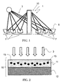
- FIG.1 schematically illustrates an example of a schematic of a concentrated solar power (CSP) plant with a solar power tower 1.
- CSP concentrated solar power
- heliostats 7 supporting mirrors 9 that may be driven by motors in order to reflect and focus the incoming sun rays on a small area at the top of the solar sun power tower 1 are arranged around the solar power tower 1.
- the concentrated heat energy may be used in a conventional power cycle or other heat engine to produce mechanical power that drives an electrical generator.
- CSP power plants can generate important amounts of power (hundreds of megawatts) for utility-scale applications.
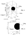
- a solar receiver 10 comprising a light absorber 11 and a heat conducting medium 12 on the back of the light absorber 11.
- the heat conducting medium 12 may be a heat conducting substrate like for example a high temperature nickel based super-alloy or a sintered silicon carbide supporting the high temperatures (for example above 650°C up to 1000°C or more) that may be generated through the absorption of concentrated sunlight and in contact with a heat conducting fluid like for example a molten salt.
- a heat conducting substrate like for example a high temperature nickel based super-alloy or a sintered silicon carbide supporting the high temperatures (for example above 650°C up to 1000°C or more) that may be generated through the absorption of concentrated sunlight and in contact with a heat conducting fluid like for example a molten salt.
- the light absorber 11 comprises nanoparticles 13 in a host material 15 which is transparent in an absorbing range of the light absorber 11.
- the nanoparticles 13 are for example metallic nanoparticles, made for instance of silver and/or of gold. Aluminum, copper, titanium, chromium or platinum may also be used.
- the host material 15 may be glass, quartz or transparent ceramic material.
- the nanoparticles 13 may be polarized polar nanoparticles, for instance made of materials supporting surface phonon-polaritons in the operating frequency range of the absorbers. For example SiC particles (resonance around 10 microns) could be used in the mid-infrared.
- the host material 15 may be for example a dielectric like SiO2.
- the nanoparticles 13 may be only out of one type of material.
- nanoparticles 13 are at least of a first material, for example gold, and a second material different from the first material, for example silver. Examples with three or four types of different materials may also be envisaged.
- the nanoparticles 13 may comprise nanoparticle of a first mean size and nanoparticles of a second mean size, different from the first mean size.
- the mean radius of said nanoparticles 13 may be less than 100nm.
- the nanoparticles 13 are for example of spherical shape, or nearly spherical shape.
- the material, size and shape of the nanoparticles 13 are chosen in order exhibit plasmonic resonances within the absorbing range of the light absorber, meaning that they exhibit plasmonic resonances as isolated nanoparticle.
- the size (radius) of nanoparticles is typically between ⁇ min /50 and ⁇ min .
- the dispersion of the nanoparticles 13 in the host material 15 is controlled in such a way that the mean distance between said nanoparticles is lower than the wavelengths of light in the absorbing range of the light absorber for generating near field radiation interactions between said nanoparticles 13.
- the mean distance between nanoparticles is smaller than the attenuation length of surface modes supported by them.
- the absorber may be obtained in a chemical way, with a coating of specialized molecules on the particles to control the distance between the nanoparticles 13. Another one is to put nanoparticles in a suspension and use a sol-gel deposition. It is also possible to deposit particles by CVD (chemical vapor deposition) with the help of chemical precursor or by laser ablation.
- CVD chemical vapor deposition
- these nanoparticles absorb at least an important part of the visible spectrum while not radiating much in the infrared range, which highly increases efficiency of the absorber, in particular for an application in a CSP plant.
- the nanoparticles 13 in the light absorber 11 are isolated from each other and from air by the host material 15, which avoids chemical interactions promoted at high temperature. There is no thin film interface that delaminates under operating conditions.
- the absorber according to the invention may be used at very high temperatures even up to 1000°C.
- the light absorber according to the invention creates and benefits from interaction modes between the nanoparticles 13 ("dressed absorption" concept). This allows the creation of multi resonant modes, promoting the absorption over a wide - yet controlled - range of wavelengths.
- the collective interactions between the nanoparticles 13 allow to maintain a strong level of absorption even in diluted lattices where the filling factor f is below 3%. Indeed, the absorption cross section of the nanoparticles 13 is strongly enhanced by the presence of neighborhood nanoparticles 13 and their interactions.
- the cutting wavelength may be defined as a wavelength where light of higher wavelength than the cutting wavelength is less absorbed than light at shorter wavelengths with respect to the cutting wavelength and the absorption coefficient decreases from the cutting wavelength to longer wavelengths.
- the invention can so be used at very high temperature.
- a unitary cell of an n-ary lattice has for example a 200nm respectively in x and y direction and 450nm in z direction.
- An example of a light absorber according the invention would be obtained through two-dimensional paving of the unitary cells.
- nanoparticle 13-Au has been chosen to have one gold nanoparticle 13-Au and one silver nanoparticle 13-Ag with a radius between 10 to 80nm and a minimal distance of at least 5nm between both nanoparticles.
- the nanoparticles 13 are immersed in a transparent material of refractive index n-1,5.
- Figures 3 and 4 show an example where a cutting wavelength of 450nm is projected.
- Figure 3 shows the unitary cell as such and figure 4 shows a top view.
- 13-Au-N and 13-Ag-N designate a gold respectively silver nanoparticle having its center in a neighboring unitary cell, but extending in the unitary cell shown.
- Figures 6 and 7 show an example where a cutting wavelength of 500nm is projected.
- Figure 6 shows the unitary cell as such and figure 7 shows a ) a top view
- 13-Au-N and 13-Ag-N designate a gold respectively silver nanoparticle having its center in a neighboring unitary cell, but extending in the unitary cell shown.
- Figures 9 and 10 show an example where a cutting wavelength of 550nm is projected.
- Figure 9 shows the unitary cell as such and figure 10 shows a top view.
- 13-Au-N and 13-Ag-N designate a gold respectively silver nanoparticle having its center in a neighboring unitary cell, but extending in the unitary cell shown.
- the light absorber according to the invention allows a quite efficient absorption in the projected absorption range and may be used at very high temperatures.
- Numerical simulations have shown that even light perturbation from a « perfect » lattice order with the unitary cells do only slightly impact the absorption curves shown in the examples above.
Landscapes
- Engineering & Computer Science (AREA)
- Physics & Mathematics (AREA)
- Chemical & Material Sciences (AREA)
- Sustainable Development (AREA)
- Sustainable Energy (AREA)
- Thermal Sciences (AREA)
- Life Sciences & Earth Sciences (AREA)
- Combustion & Propulsion (AREA)
- Mechanical Engineering (AREA)
- General Engineering & Computer Science (AREA)
- Inorganic Chemistry (AREA)
- Nanotechnology (AREA)
- Spectroscopy & Molecular Physics (AREA)
- Optical Filters (AREA)
- Photovoltaic Devices (AREA)
Priority Applications (5)
| Application Number | Priority Date | Filing Date | Title |
|---|---|---|---|
| EP13290236.2A EP2857123A1 (de) | 2013-10-04 | 2013-10-04 | Lichtabsorber |
| US15/026,804 US20160282017A1 (en) | 2013-10-04 | 2014-10-03 | Solar Thermal Receiver |
| PCT/EP2014/071273 WO2015049384A1 (en) | 2013-10-04 | 2014-10-03 | Solar thermal receiver |
| EP14780529.5A EP3052261A1 (de) | 2013-10-04 | 2014-10-03 | Solarthermischer empfänger |
| CA2926117A CA2926117A1 (en) | 2013-10-04 | 2014-10-03 | Solar thermal receiver |
Applications Claiming Priority (1)
| Application Number | Priority Date | Filing Date | Title |
|---|---|---|---|
| EP13290236.2A EP2857123A1 (de) | 2013-10-04 | 2013-10-04 | Lichtabsorber |
Publications (1)
| Publication Number | Publication Date |
|---|---|
| EP2857123A1 true EP2857123A1 (de) | 2015-04-08 |
Family
ID=49378197
Family Applications (2)
| Application Number | Title | Priority Date | Filing Date |
|---|---|---|---|
| EP13290236.2A Withdrawn EP2857123A1 (de) | 2013-10-04 | 2013-10-04 | Lichtabsorber |
| EP14780529.5A Withdrawn EP3052261A1 (de) | 2013-10-04 | 2014-10-03 | Solarthermischer empfänger |
Family Applications After (1)
| Application Number | Title | Priority Date | Filing Date |
|---|---|---|---|
| EP14780529.5A Withdrawn EP3052261A1 (de) | 2013-10-04 | 2014-10-03 | Solarthermischer empfänger |
Country Status (4)
| Country | Link |
|---|---|
| US (1) | US20160282017A1 (de) |
| EP (2) | EP2857123A1 (de) |
| CA (1) | CA2926117A1 (de) |
| WO (1) | WO2015049384A1 (de) |
Cited By (1)
| Publication number | Priority date | Publication date | Assignee | Title |
|---|---|---|---|---|
| CN114576874A (zh) * | 2022-03-08 | 2022-06-03 | 中国科学院电工研究所 | 一种填充异形陶瓷管的太阳能热发电用固体颗粒吸热器 |
Families Citing this family (2)
| Publication number | Priority date | Publication date | Assignee | Title |
|---|---|---|---|---|
| JP6839564B2 (ja) * | 2017-02-22 | 2021-03-10 | 日本碍子株式会社 | 流体加熱部材、加熱された流体を製造する装置および気体を製造する装置 |
| US11198807B2 (en) * | 2019-09-23 | 2021-12-14 | International Business Machines Corporation | Thermal interface materials with radiative coupling heat transfer |
Citations (3)
| Publication number | Priority date | Publication date | Assignee | Title |
|---|---|---|---|---|
| WO2006122222A2 (en) * | 2005-05-11 | 2006-11-16 | Georgia Tech Research Corporation | Shape tunable plasmonic nanoparticles |
| WO2009105662A1 (en) * | 2008-02-21 | 2009-08-27 | Immunolight, Llc. | Methods and systems for treating cell proliferation disorders using plasmonics enhanced photospectral therapy (pepst) and exciton-plasmon enhanced phototherapy (epep) |
| US20130092221A1 (en) * | 2011-10-14 | 2013-04-18 | Universidad Politecnica De Madrid | Intermediate band solar cell having solution-processed colloidal quantum dots and metal nanoparticles |
Family Cites Families (1)
| Publication number | Priority date | Publication date | Assignee | Title |
|---|---|---|---|---|
| US20130220312A1 (en) * | 2012-01-05 | 2013-08-29 | Norwich Technologies, Inc. | Cavity Receivers for Parabolic Solar Troughs |
-
2013
- 2013-10-04 EP EP13290236.2A patent/EP2857123A1/de not_active Withdrawn
-
2014
- 2014-10-03 US US15/026,804 patent/US20160282017A1/en not_active Abandoned
- 2014-10-03 WO PCT/EP2014/071273 patent/WO2015049384A1/en not_active Ceased
- 2014-10-03 EP EP14780529.5A patent/EP3052261A1/de not_active Withdrawn
- 2014-10-03 CA CA2926117A patent/CA2926117A1/en not_active Abandoned
Patent Citations (3)
| Publication number | Priority date | Publication date | Assignee | Title |
|---|---|---|---|---|
| WO2006122222A2 (en) * | 2005-05-11 | 2006-11-16 | Georgia Tech Research Corporation | Shape tunable plasmonic nanoparticles |
| WO2009105662A1 (en) * | 2008-02-21 | 2009-08-27 | Immunolight, Llc. | Methods and systems for treating cell proliferation disorders using plasmonics enhanced photospectral therapy (pepst) and exciton-plasmon enhanced phototherapy (epep) |
| US20130092221A1 (en) * | 2011-10-14 | 2013-04-18 | Universidad Politecnica De Madrid | Intermediate band solar cell having solution-processed colloidal quantum dots and metal nanoparticles |
Non-Patent Citations (13)
| Title |
|---|
| A. MOREAU; C. CIRACI; J.J. MOCK; R. T. HILL; Q. WANG; B.J. WILEY; A. CHILKOTI; D. R. SMITH, NATURE, vol. 492, 2012, pages 86 - 89 |
| C.E. KENNEDY: "Review of Mid to High Temperature Solar Selective Absorber Materials", NREL, July 2002 (2002-07-01) |
| G. D. MAHAN, PHYS. REV. B, vol. 38, no. 14, 1988, pages 9500 |
| HEDAYATI, M.K.; JAVAHERIRAHIM, M.; MOZOONI, B.; ABDELAZIZ, R.; TAVASSOLIZADEH, A.; CHAKRAVADHANULA, V.S.K.; ZAPOROJTCHENKO, V.; ST: "Advanced Materials", 2011, WILEY, article "Design of a perfect black absorber at visible frequenscies using plamonic metamaterials" |
| K. AYDIN; V. E. FERRY; R. M. BRIGGS; H. A. ALWATER, NAT. COMMS., vol. 2, 2011, pages 517 |
| L. LI; K.-.Q. PENG; B. HU; X. WANG; Y. HU; X.-L. WU, APPL. PHYS. LETT., vol. 100, 2012, pages 223902 |
| M. GOMEZ; L. FONSECA; G; RODRIGUEZ, FERROELECTRICS LETTERS SECTION, vol. 2, no. 1, 1984, pages 17 - 24 |
| MASSIOT ET AL., APPPL. PHYS. LETT., vol. 101, 2012, pages 163901 |
| P. ZHU ET AL., APPL. PHYS. LETT., vol. 101, 2012, pages 241116 |
| S. CHEN ET AL., APPL. PHYS. LETT., vol. 99, 2011, pages 253104 |
| S. GRÉSILLON; L. AIGOUY; A. C. BOCCARA; J. C. RIVOAL; X.QUELIN; C. DESMARESL; P. GADENNE; V. A. SHUBIN; A. K. SARYCHEV; V. M. SHA, PHYS. REV. LETT., vol. 82, 1999, pages 4520 |
| T.V. TEPERIK ET AL., NAT. PHOTONICS, vol. 2, 2008, pages 299 - 301 |
| V. M. SHALAEV; A. K. SARYCHEV, PHYS. REV. B, vol. 57, 1998, pages 13265 |
Cited By (2)
| Publication number | Priority date | Publication date | Assignee | Title |
|---|---|---|---|---|
| CN114576874A (zh) * | 2022-03-08 | 2022-06-03 | 中国科学院电工研究所 | 一种填充异形陶瓷管的太阳能热发电用固体颗粒吸热器 |
| CN114576874B (zh) * | 2022-03-08 | 2023-10-31 | 中国科学院电工研究所 | 一种填充异形陶瓷管的太阳能热发电用固体颗粒吸热器 |
Also Published As
| Publication number | Publication date |
|---|---|
| WO2015049384A1 (en) | 2015-04-09 |
| CA2926117A1 (en) | 2015-04-09 |
| US20160282017A1 (en) | 2016-09-29 |
| EP3052261A1 (de) | 2016-08-10 |
Similar Documents
| Publication | Publication Date | Title |
|---|---|---|
| Mehrabi et al. | Ultra-broadband nanostructured metamaterial absorber based on stacked square-layers of TiN/TiO2 | |
| Sakakibara et al. | Practical emitters for thermophotovoltaics: a review | |
| Wang et al. | Solar thermophotovoltaics: Progress, challenges, and opportunities | |
| Masoudian Saadabad et al. | Polarization-independent perfect absorber enabled by quasibound states in the continuum | |
| Li et al. | Nanophotonic control of thermal radiation for energy applications | |
| Wang et al. | Perfect selective metamaterial solar absorbers | |
| Wang et al. | Titanium-nitride-based integrated plasmonic absorber/emitter for solar thermophotovoltaic application | |
| Xu et al. | Enhanced photon collection in luminescent solar concentrators with distributed Bragg reflectors | |
| Li et al. | Wavelength-selective mid-infrared metamaterial absorbers with multiple tungsten cross resonators | |
| Pfiester et al. | Selective emitters for thermophotovoltaic applications | |
| Cao et al. | Mid-infrared tunable polarization-independent perfect absorber using a phase-change metamaterial | |
| JP5089605B2 (ja) | 三重接合太陽電池のためのノッチフィルタ | |
| CN110187419B (zh) | 一种基于半导体超表面的可见光宽带完美吸收器 | |
| Shameli et al. | Absorption enhancement in thin-film solar cells using an integrated metasurface lens | |
| Liu et al. | Dual broadband near-infrared perfect absorber based on a hybrid plasmonic-photonic microstructure | |
| Wang et al. | Micro/nanostructures for far-field thermal emission control: an overview | |
| Du John et al. | Design of Si based nano strip resonator with polarization-insensitive metamaterial (MTM) absorber on a glass substrate | |
| Bora et al. | Plasmonic black metals in resonant nanocavities | |
| Kim et al. | Design of a high-performance titanium nitride metastructure-based solar absorber using quantum computing-assisted optimization | |
| Wang et al. | Ultra-broadband nanowire metamaterial absorber | |
| Lu et al. | Asymmetric metasurface structures for light absorption enhancement in thin film silicon solar cell | |
| Liu et al. | Fabry–Perot-resonator-coupled metal pattern metamaterial for infrared suppression and radiative cooling | |
| EP2857123A1 (de) | Lichtabsorber | |
| Cho et al. | Optical tunneling mediated sub-skin-depth high emissivity tungsten radiators | |
| Liao et al. | Ultra-broadband solar light wave trapping by gradient cavity-thin-film metasurface |
Legal Events
| Date | Code | Title | Description |
|---|---|---|---|
| PUAI | Public reference made under article 153(3) epc to a published international application that has entered the european phase |
Free format text: ORIGINAL CODE: 0009012 |
|
| 17P | Request for examination filed |
Effective date: 20131004 |
|
| AK | Designated contracting states |
Kind code of ref document: A1 Designated state(s): AL AT BE BG CH CY CZ DE DK EE ES FI FR GB GR HR HU IE IS IT LI LT LU LV MC MK MT NL NO PL PT RO RS SE SI SK SM TR |
|
| AX | Request for extension of the european patent |
Extension state: BA ME |
|
| STAA | Information on the status of an ep patent application or granted ep patent |
Free format text: STATUS: THE APPLICATION IS DEEMED TO BE WITHDRAWN |
|
| 18D | Application deemed to be withdrawn |
Effective date: 20151009 |