EP2860742A2 - Mehrschichtige keramische elektronische Komponente und Leiterplatte, worauf diese montiert ist - Google Patents
Mehrschichtige keramische elektronische Komponente und Leiterplatte, worauf diese montiert ist Download PDFInfo
- Publication number
- EP2860742A2 EP2860742A2 EP20140275146 EP14275146A EP2860742A2 EP 2860742 A2 EP2860742 A2 EP 2860742A2 EP 20140275146 EP20140275146 EP 20140275146 EP 14275146 A EP14275146 A EP 14275146A EP 2860742 A2 EP2860742 A2 EP 2860742A2
- Authority
- EP
- European Patent Office
- Prior art keywords
- internal electrodes
- electronic component
- width
- ceramic body
- multilayer
- Prior art date
- Legal status (The legal status is an assumption and is not a legal conclusion. Google has not performed a legal analysis and makes no representation as to the accuracy of the status listed.)
- Withdrawn
Links
- 239000000919 ceramic Substances 0.000 title claims abstract description 217
- 230000003247 decreasing effect Effects 0.000 claims description 49
- 230000005534 acoustic noise Effects 0.000 claims description 48
- 229910052751 metal Inorganic materials 0.000 claims description 5
- 239000002184 metal Substances 0.000 claims description 5
- 229910052759 nickel Inorganic materials 0.000 claims description 5
- 229910052804 chromium Inorganic materials 0.000 claims description 3
- 238000010330 laser marking Methods 0.000 claims description 3
- 229910052748 manganese Inorganic materials 0.000 claims description 3
- 229910052720 vanadium Inorganic materials 0.000 claims description 3
- 239000003985 ceramic capacitor Substances 0.000 description 40
- PXHVJJICTQNCMI-UHFFFAOYSA-N nickel Substances [Ni] PXHVJJICTQNCMI-UHFFFAOYSA-N 0.000 description 9
- 238000000034 method Methods 0.000 description 7
- 230000000694 effects Effects 0.000 description 6
- 239000000843 powder Substances 0.000 description 6
- 229910002113 barium titanate Inorganic materials 0.000 description 4
- 239000010949 copper Substances 0.000 description 4
- 238000004519 manufacturing process Methods 0.000 description 4
- KDLHZDBZIXYQEI-UHFFFAOYSA-N Palladium Chemical compound [Pd] KDLHZDBZIXYQEI-UHFFFAOYSA-N 0.000 description 3
- 230000000052 comparative effect Effects 0.000 description 3
- RYGMFSIKBFXOCR-UHFFFAOYSA-N Copper Chemical compound [Cu] RYGMFSIKBFXOCR-UHFFFAOYSA-N 0.000 description 2
- JRPBQTZRNDNNOP-UHFFFAOYSA-N barium titanate Chemical compound [Ba+2].[Ba+2].[O-][Ti]([O-])([O-])[O-] JRPBQTZRNDNNOP-UHFFFAOYSA-N 0.000 description 2
- 230000008901 benefit Effects 0.000 description 2
- 230000008602 contraction Effects 0.000 description 2
- 229910052802 copper Inorganic materials 0.000 description 2
- 238000010304 firing Methods 0.000 description 2
- 238000010030 laminating Methods 0.000 description 2
- SWELZOZIOHGSPA-UHFFFAOYSA-N palladium silver Chemical compound [Pd].[Ag] SWELZOZIOHGSPA-UHFFFAOYSA-N 0.000 description 2
- 239000002245 particle Substances 0.000 description 2
- 229910000679 solder Inorganic materials 0.000 description 2
- BQCADISMDOOEFD-UHFFFAOYSA-N Silver Chemical compound [Ag] BQCADISMDOOEFD-UHFFFAOYSA-N 0.000 description 1
- 229910045601 alloy Inorganic materials 0.000 description 1
- 239000000956 alloy Substances 0.000 description 1
- 239000004020 conductor Substances 0.000 description 1
- 238000013461 design Methods 0.000 description 1
- 239000011521 glass Substances 0.000 description 1
- 239000000463 material Substances 0.000 description 1
- 239000007769 metal material Substances 0.000 description 1
- 238000012986 modification Methods 0.000 description 1
- 230000004048 modification Effects 0.000 description 1
- 229910000510 noble metal Inorganic materials 0.000 description 1
- -1 or the like Substances 0.000 description 1
- 229910052763 palladium Inorganic materials 0.000 description 1
- 238000007747 plating Methods 0.000 description 1
- 238000005498 polishing Methods 0.000 description 1
- 238000007517 polishing process Methods 0.000 description 1
- 238000007639 printing Methods 0.000 description 1
- 238000011160 research Methods 0.000 description 1
- 238000007650 screen-printing Methods 0.000 description 1
- 229910052709 silver Inorganic materials 0.000 description 1
- 239000004332 silver Substances 0.000 description 1
- 238000005245 sintering Methods 0.000 description 1
- 239000002002 slurry Substances 0.000 description 1
- VEALVRVVWBQVSL-UHFFFAOYSA-N strontium titanate Chemical compound [Sr+2].[O-][Ti]([O-])=O VEALVRVVWBQVSL-UHFFFAOYSA-N 0.000 description 1
- 238000012360 testing method Methods 0.000 description 1
Images



Classifications
-
- H—ELECTRICITY
- H01—ELECTRIC ELEMENTS
- H01G—CAPACITORS; CAPACITORS, RECTIFIERS, DETECTORS, SWITCHING DEVICES, LIGHT-SENSITIVE OR TEMPERATURE-SENSITIVE DEVICES OF THE ELECTROLYTIC TYPE
- H01G2/00—Details of capacitors not covered by a single one of groups H01G4/00-H01G11/00
- H01G2/02—Mountings
- H01G2/06—Mountings specially adapted for mounting on a printed-circuit support
-
- H—ELECTRICITY
- H01—ELECTRIC ELEMENTS
- H01G—CAPACITORS; CAPACITORS, RECTIFIERS, DETECTORS, SWITCHING DEVICES, LIGHT-SENSITIVE OR TEMPERATURE-SENSITIVE DEVICES OF THE ELECTROLYTIC TYPE
- H01G4/00—Fixed capacitors; Processes of their manufacture
- H01G4/30—Stacked capacitors
-
- H—ELECTRICITY
- H01—ELECTRIC ELEMENTS
- H01G—CAPACITORS; CAPACITORS, RECTIFIERS, DETECTORS, SWITCHING DEVICES, LIGHT-SENSITIVE OR TEMPERATURE-SENSITIVE DEVICES OF THE ELECTROLYTIC TYPE
- H01G2/00—Details of capacitors not covered by a single one of groups H01G4/00-H01G11/00
- H01G2/02—Mountings
- H01G2/06—Mountings specially adapted for mounting on a printed-circuit support
- H01G2/065—Mountings specially adapted for mounting on a printed-circuit support for surface mounting, e.g. chip capacitors
-
- H—ELECTRICITY
- H01—ELECTRIC ELEMENTS
- H01G—CAPACITORS; CAPACITORS, RECTIFIERS, DETECTORS, SWITCHING DEVICES, LIGHT-SENSITIVE OR TEMPERATURE-SENSITIVE DEVICES OF THE ELECTROLYTIC TYPE
- H01G4/00—Fixed capacitors; Processes of their manufacture
- H01G4/002—Details
- H01G4/005—Electrodes
-
- H—ELECTRICITY
- H01—ELECTRIC ELEMENTS
- H01G—CAPACITORS; CAPACITORS, RECTIFIERS, DETECTORS, SWITCHING DEVICES, LIGHT-SENSITIVE OR TEMPERATURE-SENSITIVE DEVICES OF THE ELECTROLYTIC TYPE
- H01G4/00—Fixed capacitors; Processes of their manufacture
- H01G4/002—Details
- H01G4/005—Electrodes
- H01G4/012—Form of non-self-supporting electrodes
-
- H—ELECTRICITY
- H01—ELECTRIC ELEMENTS
- H01G—CAPACITORS; CAPACITORS, RECTIFIERS, DETECTORS, SWITCHING DEVICES, LIGHT-SENSITIVE OR TEMPERATURE-SENSITIVE DEVICES OF THE ELECTROLYTIC TYPE
- H01G4/00—Fixed capacitors; Processes of their manufacture
- H01G4/002—Details
- H01G4/018—Dielectrics
- H01G4/06—Solid dielectrics
- H01G4/08—Inorganic dielectrics
- H01G4/12—Ceramic dielectrics
-
- H—ELECTRICITY
- H01—ELECTRIC ELEMENTS
- H01G—CAPACITORS; CAPACITORS, RECTIFIERS, DETECTORS, SWITCHING DEVICES, LIGHT-SENSITIVE OR TEMPERATURE-SENSITIVE DEVICES OF THE ELECTROLYTIC TYPE
- H01G4/00—Fixed capacitors; Processes of their manufacture
- H01G4/002—Details
- H01G4/228—Terminals
- H01G4/248—Terminals the terminals embracing or surrounding the capacitive element, e.g. caps
-
- H—ELECTRICITY
- H01—ELECTRIC ELEMENTS
- H01G—CAPACITORS; CAPACITORS, RECTIFIERS, DETECTORS, SWITCHING DEVICES, LIGHT-SENSITIVE OR TEMPERATURE-SENSITIVE DEVICES OF THE ELECTROLYTIC TYPE
- H01G4/00—Fixed capacitors; Processes of their manufacture
- H01G4/35—Feed-through capacitors or anti-noise capacitors
Definitions
- the present disclosure relates to a multilayer ceramic electronic component and a board having the same mounted thereon.
- the number of stacked layers has been increased in order to implement high capacitance.
- the multilayer ceramic electronic component may be manufactured to have an increased thickness as compared with a width thereof, such that high capacitance may be implemented.
- the dielectric layers have piezoelectric and electrostrictive characteristics, a piezoelectric phenomenon is generated between the internal electrodes when direct current (DC) or alternating current (AC) voltage is applied to a multilayer ceramic capacitor, such that vibrations may be generated.
- vibrations may be transferred to a printed circuit board on which the multilayer ceramic capacitor is mounted through a solder connected to the multilayer ceramic capacitor, such that the entirety of the printed circuit board becomes a sound radiating surface generating a vibration sound, which is noise.
- the vibration sound may correspond to an audio frequency range of 20 Hz to 20000 Hz making persons uncomfortable.
- the vibration sound making the persons uncomfortable as described above may be referred to as acoustic noise.
- Patent Document 1 Japanese Patent Laid-Open Publication No. 2005-129802
- An aspect of the present disclosure provides a multilayer ceramic electronic component capable of having high capacitance and reducing acoustic noise, and a board having the same mounted thereon.
- a multilayer ceramic electronic component includes: a ceramic body including dielectric layers and satisfying T/W > 1.0 when a width thereof is W and a thickness thereof is T; and first and second internal electrodes stacked to face each other, having the dielectric layer interposed therebetween, within the ceramic body, wherein when an average width of the first and second internal electrodes stacked at an upper portion of the ceramic body in a thickness direction is M1 and an average width of the first and second internal electrodes stacked at a lower portion of the ceramic body in the thickness direction is M2, M1 > M2 is satisfied.
- M1 and M2 satisfy 0.85 ⁇ M2/M1 ⁇ 0.97.
- Widths of the first and second internal electrodes may be gradually decreased.
- Widths of the first and second internal electrodes may be uniform at the upper portion of the ceramic body in the thickness direction and may be gradually decreased at the lower portion of the ceramic body in the thickness direction.
- Widths of the first and second internal electrodes may be decreased while forming a step.
- Widths of the first and second internal electrodes may be uniform at the upper portion of the ceramic body in the thickness direction and may be decreased to form a step at the lower portion of the ceramic body in the thickness direction.
- Widths of the first and second internal electrodes may be uniform at the upper portion of the ceramic body and part of the lower portion adjacent thereto and may be decreased at a remaining part of the lower portion.
- the width and the thickness of the ceramic body satisfy 1.2 ⁇ T/W ⁇ 3.0.
- the ceramic body may include a distinguishing part for distinguishing the upper and lower portions of the ceramic body from each other.
- the distinguishing part may include a dielectric layer to which at least one metal selected from a group consisting of Ni, Mn, Cr, and V is added.
- the distinguishing part may be a mark generated by laser marking.
- the dielectric layers may be stacked in an amount of 500 or more layers.
- the first and second internal electrodes may be stacked in the thickness direction of the ceramic body.
- a multilayer ceramic electronic component includes: a ceramic body including dielectric layers, satisfying T/W > 1.0 when a width thereof is W and a thickness thereof is T, and having first and second side surfaces opposing each other in a width direction; first and second internal electrodes stacked to face each other, having the dielectric layer interposed therebetween, within the ceramic body; a first side margin part formed between one sides of the first and second internal electrodes in the width direction and the first side surface and including a first acoustic noise decreasing part positioned at a lower portion thereof; and a second side margin part formed between the other sides of the first and second internal electrodes in the width direction and the second side surface and including a second acoustic noise decreasing part positioned at a lower portion thereof.
- An average width of the first and second acoustic noise decreasing parts may be wider than that of the first and second side margin parts.
- Widths of the first and second internal electrodes may be gradually decreased.
- a multilayer ceramic electronic component includes: a ceramic body including dielectric layers and satisfying T/W > 1.0 when a width thereof is W and a thickness thereof is T; and first and second internal electrodes stacked to face each other, having the dielectric layer interposed therebetween, within the ceramic body, wherein when an average width of the first and second internal electrodes stacked at an upper portion of the ceramic body in a thickness direction is M1 and an average width of the first and second internal electrodes stacked at a lower portion of the ceramic body in the thickness direction is M2, an M2/M1 value is in a range in which acoustic noise is less than 20dB and a capacitance decrease rate is less than 8%.
- a board having a multilayer ceramic electronic component mounted thereon includes: a printed circuit board having first and second electrode pads disposed thereon; and the multilayer ceramic electronic component mounted on the printed circuit board, wherein the multilayer ceramic electronic component includes a ceramic body including dielectric layers and satisfying T/W > 1.0 when a width thereof is W and a thickness thereof is T, and first and second internal electrodes stacked to face each other, having the dielectric layer interposed therebetween, within the ceramic body, and when an average width of the first and second internal electrodes stacked at an upper portion of the ceramic body in a thickness direction is M1 and an average width of the first and second internal electrodes stacked at a lower portion of the ceramic body in the thickness direction is M2, M1 > M2 is satisfied.
- a board having a multilayer ceramic electronic component mounted thereon includes: a printed circuit board having first and second electrode pads disposed thereon; and the multilayered ceramic electronic component mounted on the printed circuit board, wherein the multilayer ceramic electronic component includes: a ceramic body including dielectric layers, satisfying T/W > 1.0 when a width thereof is W and a thickness thereof is T, and having first and second side surfaces opposing each other in a width direction; first and second internal electrodes stacked to face each other, having the dielectric layer interposed therebetween, within the ceramic body; a first side margin part formed between one sides of the first and second internal electrodes in the width direction and the first side surface and including a first acoustic noise decreasing part positioned at a lower portion thereof; and a second side margin part formed between the other sides of the first and second internal electrodes in the width direction and the second side surface and including a second acoustic noise decreasing part positioned at a lower portion thereof.
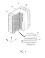
- FIG. 1 is a partially cut-away perspective view schematically showing a multilayer ceramic capacitor according to an exemplary embodiment of the present disclosure.
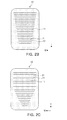
- FIG. 2A is a cross-sectional view of the multilayer ceramic capacitor of FIG. 1 , taken in a width-thickness direction.
- the multilayer ceramic electronic component may include a ceramic body 10 including dielectric layers 11, satisfying the following equation: T/W > 1.0 when a width thereof is W and a thickness thereof is T, and having a hexahedral shape; and first and second internal electrodes 21 and 22 stacked to face each other, having the dielectric layer interposed therebetween, within the ceramic body 10, wherein when an average width of the first and second internal electrodes stacked at an upper portion T1 of the ceramic body in a thickness direction is M1 and an average width of the first and second internal electrodes stacked at a lower portion T2 of the ceramic body in the thickness direction is M2, the following equation: M1>M2 is satisfied.
- a shape of the ceramic body 1.0 is not particularly limited.
- the ceramic body 10 may have a hexahedral shape.
- a "length direction” refers to an "L” direction of FIG. 1
- a "width direction” refers to a “W” direction of FIG. 1
- a “thickness direction” refers to a “T” direction of FIG. 1 .
- the "thickness direction” refers to a direction in which the dielectric layers are stacked, that is, a "stacked direction.”
- the ceramic body 10 has first and second side surfaces opposing each other in the width direction, first and second end surfaces opposing each other in the length direction, and first and second main surfaces opposing each other in the thickness direction.
- the first and second main surfaces refer to upper and lower surfaces.
- the multilayer ceramic capacitor 1 includes the ceramic body 10 including the dielectric layers 11, satisfying the following equation: T/W > 1.0 when a width thereof is W and a thickness thereof is T, and having a hexahedral shape; and the first and second internal electrodes 21 and 22 stacked to face each other, having the dielectric layer 11 interposed therebetween, within the ceramic body 10.
- the ceramic body 10 includes an upper cover layer disposed on the uppermost internal electrode and a lower cover layer disposed below the lowermost internal electrode in order to protect the internal electrodes from external impact.
- the upper and lower cover layers may be formed of the same material as that of the dielectric layers.
- the first and second internal electrodes 21 and 22 are not particularly limited, and, for example, may be formed of a conductive paste formed of at least one selected from a group consisting of a noble metal material such as palladium (Pd), a palladium-silver (Pd-Ag) alloy, or the like, nickel (Ni) and copper (Cu).
- a noble metal material such as palladium (Pd), a palladium-silver (Pd-Ag) alloy, or the like, nickel (Ni) and copper (Cu).
- the dielectric layer 11 may include ceramic powders having high permittivity, for example, barium titanate (BaTiO 3 ) based powders or strontium titanate (SrTiO 3 ) based powders.
- BaTiO 3 barium titanate
- strontium titanate (SrTiO 3 ) based powders strontium titanate
- first and second internal electrodes 21 and 22, a pair of electrodes having different polarities may be formed by printing a conductive paste including a conductive metal on the dielectric layers 11 at a predetermined thickness.
- An average thickness of the first and second internal electrodes 21 and 22 after being fired is not particularly limited as long as a capacitance may be generated.
- the average thickness may be about 0.6 ⁇ m or less.
- the average thickness of the first and second internal electrodes 21 and 22 may be measured from an image obtained by scanning a cross section of the ceramic body 10 in the width direction using a scanning electron microscope (SEM), as shown in FIG. 2A .
- SEM scanning electron microscope
- thicknesses of the dielectric layer may be measured at thirty points disposed at equal intervals in the width direction to calculate an average value thereof.
- the thirty points disposed at equal intervals may be measured in a capacitance forming part, which pertains to a region in which the first and second internal electrodes 21 and 22 are overlapped with each other.
- the average thickness of the internal electrodes may be further generalized.
- first and second internal electrodes 21 and 22 may be alternately exposed through both end surfaces of the ceramic body in a direction in which the dielectric layers 11 are stacked and be electrically insulated from each other by the dielectric layers 11 disposed therebetween.
- the first and second internal electrodes 21 and 22 are electrically connected to first and second external electrodes 31 and 32, respectively, through portions thereof alternately exposed through both end surfaces of the ceramic body 10.
- the capacitance of the multilayer ceramic capacitor 1 may be proportional to an area of the region in which the first and second internal electrodes 21 and 22 are overlapped with each other.
- the first and second external electrodes 31 and 32 may be formed on an outer portion of the ceramic body 10 and be electrically connected to the first and second internal electrodes 21 and 22, respectively.
- the first and second external electrodes 31 and 32 may be formed of the same conductive material as that of the internal electrodes, but are not limited thereto.
- the first and second external electrodes 31 and 32 may be formed of copper (Cu), silver (Ag), nickel (Ni), or the like.
- the first and second external electrodes 31 and 32 may be formed by applying and then firing a conductive paste prepared by adding a glass frit to metal powders.
- the ceramic body 10 may be formed by laminating and then firing a plurality of dielectric layers 11.
- a shape and a dimension of the ceramic body 10 and the number of stacked dielectric layers 11 are not limited to those shown in the present embodiment.
- the plurality of dielectric layers 11 forming the ceramic body 10 may be in a sintered state. Adj acent dielectric layers 11 may be integrated with each other so that boundaries therebetween are not readily apparent without using a scanning electron microscope (SEM).
- an average thickness of the dielectric layers 11 may be arbitrarily altered in accordance with a capacitance design of the multilayer ceramic capacitor 1, but is about 0.1 ⁇ m to about 0.6 ⁇ m after the dielectric layers 11 are sintered.
- the average thickness td of the dielectric layers 11 may be measured from an image obtained by scanning a cross section of the ceramic body 10 in the width direction using a scanning electron microscope (SEM) as shown in FIG. 2A , which may be performed by a method similar to the method of measuring the average thickness of the internal electrodes.
- SEM scanning electron microscope
- the number of stacked dielectric layers 11 is not particularly limited, but may be, for example, 500 or more.
- the number of stacked dielectric layers 11 may be 500 or more, whereby a high capacitance multilayer ceramic capacitor including the ceramic body having a thickness T larger than a width W may be implemented.
- the thickness T of the ceramic body 10 is larger than the width W of the ceramic body 10.
- a general multilayer ceramic capacitor has been manufactured to have a width and a thickness substantially identical to each other.
- the multilayer ceramic capacitor according to the exemplary embodiment of the present disclosure is miniaturized, a sufficient space may be secured when the multilayer ceramic capacitor is mounted on a board. Therefore, the number of stacked layers may be increased in order to implement a high capacitance multilayer ceramic capacitor.
- the ceramic body 10 may be configured to have a ratio of the thickness to the width T/W satisfying the following equation: 1.2 ⁇ T/W ⁇ 3.0.
- the multilayer ceramic capacitor is manufactured to have the relationship between the thickness T and the width W of the ceramic body satisfying the following equation: T/W > 1.0, acoustic noise due to a piezoelectric phenomenon may be further increased when the multilayer ceramic capacitor is mounted on the board.
- widths of the internal electrodes and margin parts may be controlled, whereby a multilayer ceramic capacitor having decreased acoustic noise is obtained.
- the ceramic body When voltages having different polarities are applied to the first and second external electrodes formed on both end portions of the ceramic body, the ceramic body may be expanded and contracted in the thickness direction by an inverse piezoelectric effect of the dielectric layers 11, and both end portions of the first and second external electrodes may be contracted and expanded as opposed to the expansion and the contraction of the ceramic body in the thickness direction, by a Poisson effect. Vibrations of the multilayer ceramic capacitor caused by the contraction and the expansion of the ceramic body and the first and second external electrodes may be transferred to the board, and the board may become a sound radiating surface of the vibrations to generate noise, which is referred to as acoustic noise.
- the internal electrodes 21 and 22 may be formed so that when an average width of the first and second internal electrodes stacked at the upper portion Tl of the ceramic body in the thickness direction is M1 and an average width of the first and second internal electrodes 21 and 22 stacked at the lower portion T2 of the ceramic body in the thickness direction is M2, the following equation: M1 > M2 is satisfied.
- the width of the internal electrode was measured as a distance W E between both sides of the internal electrode in the width direction.
- the upper portion and the lower portion of the ceramic body in the thickness direction may be divided based on a point corresponding to a half of the thickness of the ceramic body.
- Widths of the internal electrodes formed at the upper portion and the lower portion of the ceramic body are different from each other, so that distances from the sides of the internal electrodes to the first and second side surfaces of the ceramic body at the upper portion and the lower portion thereof may be different from each other. Therefore, deformation rates at the upper portion and the lower portion of the ceramic body depending on the inverse piezoelectric effect are different from each other, so that the acoustic noise may be decreased. That is, the width of the internal electrode at the lower portion of the ceramic body may be decreased to decrease the deformation rate at the lower portion of the ceramic body. In the case in which the deformation rate at the lower portion of the ceramic body adjacent to the board is decreased, the vibrations transferred to the board are decreased, so that the acoustic noise is decreased.
- the width of the internal electrode formed at the upper portion of the ceramic body may be wider than that of the internal electrode formed at the lower portion of the ceramic body, thereby substantially minimizing a capacitance decrease while decreasing the acoustic noise.
- M1 and M2 satisfy the following equation: 0.85 ⁇ M2/M1 ⁇ 0.97.
- a decrease effect of the acoustic noise may not be substantially large, and in the case in which M2/M1 is in the range of 0.85 to 0.97, the acoustic noise is significantly decreased.
- M2/M1 is less than 0.85, which is a boundary value, the decrease effect of the acoustic noise may not be significantly improved as compared with the case in which M2/M1 is in the range of 0.85 to 0.97 but a capacitance may be continuously decreased.
- the internal electrodes it advantageous for the internal electrodes to be formed so that M1 and M2 satisfy the following equation: 0.85 ⁇ M2/M1 ⁇ 0.97, in view of minimizing the acoustic noise and the capacitance decrease.
- a multilayer ceramic electronic component may include a ceramic body 10 including dielectric layers 11, satisfying the following equation: T/W > 1.0 when a width thereof is W and a thickness thereof is T, having first and second side surfaces opposing each other in a width direction, and having a hexahedral shape; first and second internal electrodes 21 and 22 stacked to face each other, having the dielectric layer interposed therebetween, within the ceramic body 10; a first side margin part 41 formed between one sides of the first and second internal electrodes in the width direction and the first side surface and including a first acoustic noise decreasing part 41' positioned at a lower portion thereof; and a second side margin part 42 formed between the other sides of the first and second internal electrodes in the width direction and the second side surface and including a second acoustic noise decreasing part 42' positioned at a lower portion thereof.
- Widths of the first side margin part formed between one sides of the first and second internal electrodes in the width direction and the first side surface and the second side margin part formed between the other sides of the first and second internal electrodes in the width direction and the second side surface may be controlled to thereby decrease acoustic noise.
- the first and second side margin parts 41 and 42 may include the acoustic noise decreasing parts 41' and 42' positioned at the lower portions thereof, respectively. Average widths of the acoustic noise decreasing parts may be wider than those of the first and second side margin parts.
- the first and second side margin parts may include wide side margin parts (acoustic noise decreasing parts) positioned at the lower portions thereof, to decrease the deformation rate at the lower portion of the ceramic body, thereby decreasing the acoustic noise.
- the widths of the side margin parts in a direction perpendicular to a direction in which the first and second internal electrodes are exposed are different from each other to differently control the deformation rates at the upper portion and the lower portion of the ceramic body in a direction in which the internal electrodes are stacked, whereby the acoustic noise is decreased.
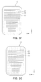
- FIGS. 2B through 2G are cross-sectional views of multilayer ceramic capacitors according to exemplary embodiments of the present disclosure, taken in a width-thickness direction.
- widths of the first and second internal electrodes 21 and 22 may be gradually decreased from an upper portion of the ceramic body in the stacked direction toward a lower portion thereof.
- the entire contour of the internal electrodes represented by a W-T cross section of the ceramic body may have an inverse trapezoidal shape in which the widths thereof are decreased toward the lower portion.
- the first and second internal electrodes 21 and 22 may have uniform widths at the upper portion of the ceramic body and have widths gradually narrowing toward a bottom surface of the ceramic body at the lower portion of the ceramic body.
- widths of the first and second internal electrodes 21 and 22 may be relatively wide at the upper portion of the ceramic body and part of the lower portion adjacent thereto, and widths of the first and second internal electrodes 21 and 22 may be relatively narrow at the remaining part of the lower portion of the ceramic body.
- widths of the first and second internal electrodes 21 and 22 may be relatively wide at the upper portion of the ceramic body and part of the lower portion adjacent thereto, and widths of the first and second internal electrodes 21 and 22 may be relatively narrow at the remaining part of the lower portion of the ceramic body and may gradually become narrower toward the bottom surface of the ceramic body.
- the first and second internal electrodes 21 and 22 may be relatively wide at the upper portion of the ceramic body, and the first and second internal electrodes 21 and 22 may be relatively narrow at the lower portion of the ceramic body, wherein the widths of the first and second internal electrodes disposed at the lower portion of the ceramic body may become narrower stepwise in two or more sections.
- widths of the first and second internal electrodes 21 and 22 may be uniformly wide at the upper portion of the ceramic body, while widths of the first and second internal electrodes 21 and 22 may be gradually decreased at part of the lower portion of the ceramic body adjacent to the upper portion of the ceramic body, and widths of the first and second internal electrodes 21 and 22 may be uniformly narrow at the remaining part of the lower portion of the ceramic body adjacent to the bottom surface of the ceramic body.
- the multilayer ceramic capacitor according to the exemplary embodiment of the present disclosure needs to be mounted on the board so that the lower portion of the ceramic body at which an average width of the internal electrodes is narrow is adjacent to the board.
- the upper cover layer or the lower cover layer of the ceramic body may include a distinguishing part (not shown) formed of a dielectric layer having a brightness or color difference.
- the distinguishing part may be a dielectric layer formed by sintering a single ceramic green sheet or laminating a plurality of ceramic green sheets.
- the dielectric layer forming the distinguishing part may have a brightness or color difference at an outer portion of the ceramic body 10 by having at least one metal selected from a group consisting of Ni, Mn, Cr, and V added thereto.
- laser marking may be performed on the upper cover layer or the lower cover layer to allow a mark or a symbol to remain on the upper cover layer or the lower cover layer even after the ceramic green sheet is sintered, thereby allowing the upper portion and the lower portion of the ceramic body to be distinguished from each other.
- a multilayer ceramic electronic component may include a ceramic body including dielectric layers, satisfying the following equation: T/W > 1.0 when a width thereof is W and a thickness thereof is T, and having a hexahedral shape; and first and second internal electrodes stacked to face each other, having the dielectric layer interposed therebetween, within the ceramic body 10, wherein when an average width of the first and second internal electrodes stacked at an upper portion of the ceramic body in a thickness direction is M1 and an average width of the first and second internal electrodes stacked at a lower portion of the ceramic body in the thickness direction is M2, an M2/M1 value is in a range in which acoustic noise is less than 20dB and a capacitance decrease rate is less than 8%.
- FIG. 3 is a perspective view of a printed circuit board on which the multilayer ceramic capacitor of FIG. 1 is mounted.
- a board 200 having a multilayer ceramic capacitor 1 mounted thereon may include a printed circuit board 210 having the multilayer ceramic capacitor 1 mounted thereon and first and second electrode pads 221 and 222 formed on an upper surface of the printed circuit board 210 so as to be spaced apart from each other.
- first and second external electrodes 31 and 32 of the multilayered ceramic capacitor 1 may be electrically connected to the printed circuit board 210 by a solder 230 in a state in which they contact the first and second electrode pads 221 and 222, respectively.
- a board having a multilayer ceramic electronic component mounted thereon may include a printed circuit board 210 having first and second electrode pads 221 and 222 disposed thereon; and the multilayer ceramic electronic component 1 mounted on the printed circuit board, wherein the multilayer ceramic electronic component includes a ceramic body including dielectric layers, satisfying the following equation: T/W > 1.0 when a width thereof is W and a thickness thereof is T, and having a hexahedral shape, and first and second internal electrodes stacked to face each other, having the dielectric layer interposed therebetween, within the ceramic body, and satisfying the following equation: M1 > M2 when an average width of the first and second internal electrodes stacked at an upper portion of the ceramic body in a thickness direction is M1 and an average width of the first and second internal electrodes stacked at a lower portion of the ceramic body in the thickness direction is M2.
- a board having a multilayer ceramic electronic component mounted thereon may include a printed circuit board 210 having first and second electrode pads 221 and 222 disposed thereon; and the multilayer ceramic electronic component 1 mounted on the printed circuit board, wherein the multilayer ceramic electronic component includes a ceramic body including dielectric layers, satisfying the following equation: T/W > 1.0 when a width thereof is W and a thickness thereof is T, having first and second side surfaces opposing each other in a width direction, and having a hexahedral shape, first and second internal electrodes stacked to face each other, having the dielectric layer interposed therebetween, within the ceramic body, a first side margin part formed between one sides of the first and second internal electrodes in the width direction and the first side surface and including a first acoustic noise decreasing part positioned at a lower portion thereof, and a second side margin part formed between the other sides of the first and second internal electrodes in the width direction and the second side surface and including a second acous
- the Experimental Example was performed in order to test an acoustic noise and whether or not a target capacitance has been implemented in a multilayer ceramic capacitor depending on an M2/M1 value when an average width of first and second internal electrodes stacked at an upper portion of a ceramic body in a thickness direction is M1 and an average width of the first and second internal electrodes stacked at a lower portion of the ceramic body in the thickness direction is M2.
- the multilayer ceramic capacitors according to Experimental Examples were manufactured as follows.
- a slurry including a powder such as a barium titanate (BaTiO 3 ) powder, or the like, having an average particle size of 0.1 ⁇ m was applied to carrier films and dried to prepare a plurality of ceramic green sheets having thicknesses of 1.05 ⁇ m and 0.95 ⁇ m, thereby forming dielectric layers.
- a powder such as a barium titanate (BaTiO 3 ) powder, or the like
- a conductive paste for internal electrodes including 40 to 50 parts by weight of a nickel powder having an average particle size of 0.1 ⁇ m to 0.2 ⁇ m was prepared.
- the conductive paste for internal electrodes was applied to the ceramic green sheets by a screen printing method to form internal electrodes, and 500 or more ceramic green sheets were stacked to manufacture a plurality of stacked bodies having different M2/M1 values.
- the stacked bodies were compressed and cut to manufacture chips of a 0603 (length ⁇ width) size having a ratio of thickness to width exceeding 1, and the chips were sintered at a temperature of 1050 °C to 1200 °C under a reducing atmosphere in which H 2 is 0.1% or less.
- a polishing process was performed on respective corners and vertices of the chips by a polishing device before the chips were sintered.
- Table 1 shows the acoustic noise and whether or not the target capacitance has been implemented in a case in which the M2/M1 value changes depending on various shapes of internal electrodes within a ceramic body.
- Sample M2/M1 Acoustic Noise (dB) Capacitance Decrease Rate (%) Capacitance Implementation 1* 0.83 15.4 8.5 NG 2* 0.84 15.8 8.0 NG 3 0.85 15.8 7.5 OK 4 0.86 16.1 7.0 OK 5 0.87 16.3 6.5 OK 6 0.88 16.3 6.0 OK 7 0.89 16.3 5.5 OK 8 0.90 16.5 5.0 OK 9 0.91 16.8 4.5 OK 10 0.92 17.1 4.0 OK 11 0.93 17.3 3.5 OK 12 0.94 17.5 3.0 OK 13 0.95 17.6 2.5 OK 14 0.96 17.9 2.0 OK 15 0.97 18.2 1.5 OK 16* 0.98 20.1 1.0 OK 17* 0.99 23 0.5 OK *: Comparative Example
- a multilayer ceramic capacitor having high capacitance and decreased acoustic noise, and a board having the same mounted thereon may be provided.
Landscapes
- Engineering & Computer Science (AREA)
- Power Engineering (AREA)
- Microelectronics & Electronic Packaging (AREA)
- Manufacturing & Machinery (AREA)
- Chemical & Material Sciences (AREA)
- Ceramic Engineering (AREA)
- Inorganic Chemistry (AREA)
- Ceramic Capacitors (AREA)
- Fixed Capacitors And Capacitor Manufacturing Machines (AREA)
Applications Claiming Priority (1)
| Application Number | Priority Date | Filing Date | Title |
|---|---|---|---|
| KR1020130111706A KR101532141B1 (ko) | 2013-09-17 | 2013-09-17 | 적층 세라믹 전자부품 및 적층 세라믹 전자부품 실장 기판 |
Publications (2)
| Publication Number | Publication Date |
|---|---|
| EP2860742A2 true EP2860742A2 (de) | 2015-04-15 |
| EP2860742A3 EP2860742A3 (de) | 2015-06-10 |
Family
ID=51063379
Family Applications (1)
| Application Number | Title | Priority Date | Filing Date |
|---|---|---|---|
| EP14275146.0A Withdrawn EP2860742A3 (de) | 2013-09-17 | 2014-07-04 | Mehrschichtige keramische elektronische Komponente und Leiterplatte, worauf diese montiert ist |
Country Status (5)
| Country | Link |
|---|---|
| US (2) | US9595386B2 (de) |
| EP (1) | EP2860742A3 (de) |
| JP (1) | JP6058591B2 (de) |
| KR (1) | KR101532141B1 (de) |
| CN (1) | CN104465085B (de) |
Families Citing this family (21)
| Publication number | Priority date | Publication date | Assignee | Title |
|---|---|---|---|---|
| JP6665438B2 (ja) * | 2015-07-17 | 2020-03-13 | 株式会社村田製作所 | 積層セラミックコンデンサ |
| JP6522549B2 (ja) * | 2016-06-07 | 2019-05-29 | 太陽誘電株式会社 | 積層セラミックコンデンサ |
| JP2018006627A (ja) | 2016-07-05 | 2018-01-11 | 太陽誘電株式会社 | 積層セラミックコンデンサ |
| JP6520861B2 (ja) * | 2016-08-10 | 2019-05-29 | 株式会社村田製作所 | 電子部品 |
| JP6939187B2 (ja) * | 2017-07-25 | 2021-09-22 | Tdk株式会社 | 電子部品及びその製造方法 |
| JP7122818B2 (ja) * | 2017-11-30 | 2022-08-22 | 太陽誘電株式会社 | 積層セラミック電子部品及びその製造方法 |
| JP7510741B2 (ja) * | 2018-08-23 | 2024-07-04 | 太陽誘電株式会社 | 積層セラミック電子部品の製造方法 |
| JP7178886B2 (ja) * | 2018-11-27 | 2022-11-28 | 太陽誘電株式会社 | 積層セラミック電子部品及び実装基板 |
| KR102724887B1 (ko) * | 2018-12-18 | 2024-11-01 | 삼성전기주식회사 | 커패시터 부품 |
| JP7374594B2 (ja) * | 2019-02-25 | 2023-11-07 | 太陽誘電株式会社 | セラミック電子部品、実装基板、セラミック電子部品の包装体、およびセラミック電子部品の製造方法 |
| JP2021027087A (ja) * | 2019-07-31 | 2021-02-22 | 太陽誘電株式会社 | 積層セラミック電子部品及び部品実装基板 |
| JP7488045B2 (ja) * | 2019-11-27 | 2024-05-21 | 太陽誘電株式会社 | 積層セラミック電子部品及びその製造方法 |
| JP7492306B2 (ja) * | 2020-05-22 | 2024-05-29 | 太陽誘電株式会社 | セラミック電子部品およびその製造方法 |
| JP2023098641A (ja) * | 2021-12-28 | 2023-07-10 | サムソン エレクトロ-メカニックス カンパニーリミテッド. | 積層型電子部品の製造方法及び積層型電子部品 |
| JP2023121897A (ja) | 2022-02-22 | 2023-09-01 | 太陽誘電株式会社 | 積層セラミックコンデンサ |
| JP2023122515A (ja) * | 2022-02-22 | 2023-09-01 | 太陽誘電株式会社 | 積層セラミックコンデンサ |
| JP2023148401A (ja) * | 2022-03-30 | 2023-10-13 | 太陽誘電株式会社 | セラミック電子部品およびその製造方法 |
| JPWO2024161743A1 (de) * | 2023-01-30 | 2024-08-08 | ||
| JP2025008880A (ja) * | 2023-07-06 | 2025-01-20 | 株式会社村田製作所 | 積層セラミックコンデンサ |
| KR20250063637A (ko) * | 2023-11-01 | 2025-05-08 | 삼성전기주식회사 | 적층형 전자 부품 |
| WO2025181944A1 (ja) * | 2024-02-28 | 2025-09-04 | 太陽誘電株式会社 | 積層セラミックコンデンサ及び積層セラミックコンデンサの製造方法 |
Citations (1)
| Publication number | Priority date | Publication date | Assignee | Title |
|---|---|---|---|---|
| JP2005129802A (ja) | 2003-10-24 | 2005-05-19 | Tdk Corp | 積層セラミックコンデンサ |
Family Cites Families (21)
| Publication number | Priority date | Publication date | Assignee | Title |
|---|---|---|---|---|
| JPH04329615A (ja) * | 1991-04-30 | 1992-11-18 | Nec Corp | 積層セラミック電子部品及びその製造方法 |
| JPH09260184A (ja) | 1996-03-19 | 1997-10-03 | Murata Mfg Co Ltd | 積層セラミックコンデンサ |
| JPH11297566A (ja) | 1998-04-07 | 1999-10-29 | Murata Mfg Co Ltd | 積層セラミック電子部品 |
| JP2000124057A (ja) * | 1998-10-12 | 2000-04-28 | Tdk Corp | 積層型セラミックコンデンサ |
| JP2004022859A (ja) * | 2002-06-18 | 2004-01-22 | Murata Mfg Co Ltd | 積層セラミックコンデンサおよびその製造方法 |
| US7092236B2 (en) * | 2005-01-20 | 2006-08-15 | Samsung Electro-Mechanics Co., Ltd. | Multilayer chip capacitor |
| JP2007103496A (ja) | 2005-09-30 | 2007-04-19 | Tdk Corp | コンデンサおよび基板アセンブリ |
| US7667949B2 (en) | 2006-08-05 | 2010-02-23 | John Maxwell | Capacitor having improved surface breakdown voltage performance and method for marking same |
| CN101868838B (zh) * | 2007-11-22 | 2011-11-09 | 株式会社村田制作所 | 层叠陶瓷电子元件 |
| CN101970373A (zh) * | 2008-02-05 | 2011-02-09 | 株式会社村田制作所 | 介电陶瓷及层叠陶瓷电容器 |
| JP2009200168A (ja) | 2008-02-20 | 2009-09-03 | Tdk Corp | セラミック電子部品、セラミック電子部品の製造方法、及びセラミック電子部品の梱包方法 |
| KR101079408B1 (ko) * | 2009-12-24 | 2011-11-02 | 삼성전기주식회사 | 적층 세라믹 커패시터 및 그 제조방법 |
| KR101158188B1 (ko) | 2010-02-01 | 2012-06-19 | 삼성전기주식회사 | 나노 입자 합성 장치 및 이를 이용한 나노 입자 합성 방법 |
| JP4941585B2 (ja) * | 2010-10-19 | 2012-05-30 | Tdk株式会社 | セラミック電子部品、セラミック電子部品の製造方法、及びセラミック電子部品の梱包方法 |
| KR101058697B1 (ko) | 2010-12-21 | 2011-08-22 | 삼성전기주식회사 | 적층 세라믹 커패시터의 회로 기판 실장 구조, 실장 방법과 이를 위한 회로 기판의 랜드 패턴, 수평 방향으로 테이핑한 적층 세라믹 커패시터의 포장체 및 수평 방향 정렬방법 |
| KR101856083B1 (ko) | 2011-05-31 | 2018-05-09 | 삼성전기주식회사 | 적층 세라믹 커패시터 |
| JP5770539B2 (ja) * | 2011-06-09 | 2015-08-26 | Tdk株式会社 | 電子部品及び電子部品の製造方法 |
| KR101539808B1 (ko) * | 2011-06-23 | 2015-07-28 | 삼성전기주식회사 | 적층 세라믹 커패시터 |
| JP5899699B2 (ja) | 2011-08-10 | 2016-04-06 | Tdk株式会社 | 積層型コンデンサ |
| KR101300359B1 (ko) | 2011-11-02 | 2013-08-28 | 삼성전기주식회사 | 적층 세라믹 전자부품 및 그 제조방법 |
| JP2013115425A (ja) * | 2011-11-30 | 2013-06-10 | Samsung Electro-Mechanics Co Ltd | 積層セラミック電子部品及びその製造方法 |
-
2013
- 2013-09-17 KR KR1020130111706A patent/KR101532141B1/ko active Active
-
2014
- 2014-07-01 JP JP2014135703A patent/JP6058591B2/ja not_active Expired - Fee Related
- 2014-07-01 US US14/321,305 patent/US9595386B2/en active Active
- 2014-07-04 EP EP14275146.0A patent/EP2860742A3/de not_active Withdrawn
- 2014-07-10 CN CN201410326571.4A patent/CN104465085B/zh not_active Expired - Fee Related
-
2016
- 2016-12-22 US US15/388,140 patent/US9875850B2/en active Active
Patent Citations (1)
| Publication number | Priority date | Publication date | Assignee | Title |
|---|---|---|---|---|
| JP2005129802A (ja) | 2003-10-24 | 2005-05-19 | Tdk Corp | 積層セラミックコンデンサ |
Also Published As
| Publication number | Publication date |
|---|---|
| KR101532141B1 (ko) | 2015-06-26 |
| US9595386B2 (en) | 2017-03-14 |
| CN104465085A (zh) | 2015-03-25 |
| US20150075854A1 (en) | 2015-03-19 |
| US20170103855A1 (en) | 2017-04-13 |
| JP6058591B2 (ja) | 2017-01-11 |
| EP2860742A3 (de) | 2015-06-10 |
| KR20150031907A (ko) | 2015-03-25 |
| JP2015061074A (ja) | 2015-03-30 |
| CN104465085B (zh) | 2017-09-29 |
| US9875850B2 (en) | 2018-01-23 |
Similar Documents
| Publication | Publication Date | Title |
|---|---|---|
| US9875850B2 (en) | Multilayer ceramic electronic component and board having the same mounted thereon | |
| EP2827351B1 (de) | Mehrschichtige keramische elektronische chip-komponent | |
| US10014112B2 (en) | Capacitor and module | |
| EP2669914B1 (de) | Mehrschichtige elektronische chip-komponente, plattine zu deren montage und verpackungseinheit dafür | |
| KR101452054B1 (ko) | 적층 세라믹 커패시터 및 그 실장 기판 | |
| US9570237B2 (en) | Multilayer ceramic capacitor and mounting board for multilayer ceramic capacitor | |
| US9330844B2 (en) | Multilayer ceramic capacitor and mounting board therefor | |
| US9779875B2 (en) | Multilayer ceramic electronic component | |
| US9099240B2 (en) | Multilayered ceramic capacitor and board for mounting the same | |
| US20140063684A1 (en) | Conductive paste composition for external electrode, multilayered ceramic component including the same and manufacturing method thereof | |
| KR101452067B1 (ko) | 적층 세라믹 커패시터 및 그 실장 기판 | |
| KR20150018650A (ko) | 적층 세라믹 전자 부품 및 그 실장 기판과 제조 방법 | |
| KR20150011263A (ko) | 적층 세라믹 커패시터 및 그 실장 기판 | |
| KR20150084078A (ko) | 적층 세라믹 커패시터 및 그 실장 기판 | |
| KR20180070866A (ko) | 적층 세라믹 커패시터 | |
| TWI488202B (zh) | 多層陶瓷電容器及製造該多層陶瓷電容器的方法 | |
| US9257234B2 (en) | Multilayer ceramic capacitor and board having the same mounted thereon | |
| KR101462759B1 (ko) | 적층 세라믹 커패시터 및 그 실장 기판 | |
| US9336944B2 (en) | Multilayer ceramic electronic component and board for mounting the same |
Legal Events
| Date | Code | Title | Description |
|---|---|---|---|
| PUAI | Public reference made under article 153(3) epc to a published international application that has entered the european phase |
Free format text: ORIGINAL CODE: 0009012 |
|
| 17P | Request for examination filed |
Effective date: 20140704 |
|
| AK | Designated contracting states |
Kind code of ref document: A2 Designated state(s): AL AT BE BG CH CY CZ DE DK EE ES FI FR GB GR HR HU IE IS IT LI LT LU LV MC MK MT NL NO PL PT RO RS SE SI SK SM TR |
|
| AX | Request for extension of the european patent |
Extension state: BA ME |
|
| PUAL | Search report despatched |
Free format text: ORIGINAL CODE: 0009013 |
|
| RIC1 | Information provided on ipc code assigned before grant |
Ipc: H01G 4/012 20060101ALI20150430BHEP Ipc: H05K 1/16 20060101ALI20150430BHEP Ipc: H01G 2/06 20060101ALI20150430BHEP Ipc: H01G 4/12 20060101ALN20150430BHEP Ipc: H05K 1/18 20060101ALI20150430BHEP Ipc: H01G 4/30 20060101AFI20150430BHEP Ipc: H01G 4/35 20060101ALI20150430BHEP |
|
| AK | Designated contracting states |
Kind code of ref document: A3 Designated state(s): AL AT BE BG CH CY CZ DE DK EE ES FI FR GB GR HR HU IE IS IT LI LT LU LV MC MK MT NL NO PL PT RO RS SE SI SK SM TR |
|
| AX | Request for extension of the european patent |
Extension state: BA ME |
|
| STAA | Information on the status of an ep patent application or granted ep patent |
Free format text: STATUS: THE APPLICATION IS DEEMED TO BE WITHDRAWN |
|
| 18D | Application deemed to be withdrawn |
Effective date: 20151211 |