EP2860875A1 - Convertisseur analogique-numérique - Google Patents
Convertisseur analogique-numérique Download PDFInfo
- Publication number
- EP2860875A1 EP2860875A1 EP20130187912 EP13187912A EP2860875A1 EP 2860875 A1 EP2860875 A1 EP 2860875A1 EP 20130187912 EP20130187912 EP 20130187912 EP 13187912 A EP13187912 A EP 13187912A EP 2860875 A1 EP2860875 A1 EP 2860875A1
- Authority
- EP
- European Patent Office
- Prior art keywords
- digital
- output
- input
- converter
- analogue
- Prior art date
- Legal status (The legal status is an assumption and is not a legal conclusion. Google has not performed a legal analysis and makes no representation as to the accuracy of the status listed.)
- Granted
Links
Images

Classifications
-
- H—ELECTRICITY
- H03—ELECTRONIC CIRCUITRY
- H03M—CODING; DECODING; CODE CONVERSION IN GENERAL
- H03M3/00—Conversion of analogue values to or from differential modulation
- H03M3/30—Delta-sigma modulation
- H03M3/458—Analogue/digital converters using delta-sigma modulation as an intermediate step
- H03M3/494—Sampling or signal conditioning arrangements specially adapted for delta-sigma type analogue/digital conversion systems
- H03M3/496—Details of sampling arrangements or methods
-
- H—ELECTRICITY
- H03—ELECTRONIC CIRCUITRY
- H03M—CODING; DECODING; CODE CONVERSION IN GENERAL
- H03M3/00—Conversion of analogue values to or from differential modulation
- H03M3/30—Delta-sigma modulation
- H03M3/39—Structural details of delta-sigma modulators, e.g. incremental delta-sigma modulators
-
- H—ELECTRICITY
- H03—ELECTRONIC CIRCUITRY
- H03M—CODING; DECODING; CODE CONVERSION IN GENERAL
- H03M3/00—Conversion of analogue values to or from differential modulation
- H03M3/30—Delta-sigma modulation
- H03M3/458—Analogue/digital converters using delta-sigma modulation as an intermediate step
- H03M3/462—Details relating to the decimation process
Definitions
- This disclosure relates to analogue to digital converters (ADCs), and particularly, although not exclusively, to ADCs, including sigma delta ADCs, that are configured to operate at low output sample rates to enable low power decimation.
- ADCs analogue to digital converters
- Sigma delta analogue to digital converters ADCs
- DACs digital to analogue converters
- Sigma delta modulation SDM may be used to encode analogue signals into digital signals. The conversion is achieved using error feedback, where the difference between the two signals is measured and used to improve the conversion.
- analogue to digital converter comprising:
- the forward (non-feedback) branch of the ADC may be considered to comprise the analogue filter, the quantizer, and the digital integrator. Splitting this forward branch into an analogue portion (comprising the filter) and a digital portion (comprising the quantizer, and the digital integrator), can allow improved scalability while stability is maintained. Parameters of the digital portion can scale with the sample rate, therefore allowing different sample rates to be used without requiring reconfiguration.
- the analogue portion can be stable under different sample rates. It may be advantageous for an ADC to be stable at different frequencies so that it may be used in different applications, for example for both speech/voice-band processing (typically operating around 8 kHz) and high-end audio applications (typically operating around 48 kHz).
- the use/amount of analogue circuitry in such an ADC may be reduced.
- the analogue circuitry in the ADC may be the analogue filter (such as a first order filter) followed by the quantizer.
- the digital integrator followed by the main feedback DAC (which may be a multi-bit DAC) are included in the ADC to increase the resolution of the circuit with multiple bits.
- the overall ADC loop may be second order.
- the digital integrator may be a multi-bit up/down counter.
- the main feedback digital to analogue converter may be configured to receive the multi-bit output signal from the digital integrator output.
- the analogue to digital converter may further comprise a digital sigma delta modulator block having a digital modulator input and a digital modulator output.
- the digital modulator input may be connected to the digital integrator output and the digital modulator output may be connected to both the output terminal and the main feedback converter input.
- the main feedback digital to analogue converter may be a finite impulse response digital to analogue converter (FIRDAC).
- FIRDAC finite impulse response digital to analogue converter
- Use of the digital sigma delta modulator block and the finite impulse response digital to analogue converter may allow for a multi-level feedback signal having sufficient resolution, that is, the overall ADC can meet a required product specification, and has a resolution such that it provides an acceptably low level of quantization noise and an adequately high dynamic range for practical use.
- the analogue to digital converter may comprise an intermediate feedback digital to analogue converter having an intermediate feedback converter input and an intermediate feedback converter output.
- the intermediate feedback converter input may be connected to the quantizer output.
- the analogue to digital converter may further comprise an intermediate summer having a first intermediate summing input, a second intermediate summing input and an intermediate summing output.
- the first intermediate summing input may be connected to the main feedback converter output.
- the second intermediate summing input may be connected to the intermediate feedback converter output.
- the intermediate summing output may be connected to the subtracting input of the main summer.
- the split/branch at the output of the quantizer creates a loop comprising the analogue filter, quantizer and intermediate feedback DAC which may be a first order loop.
- This first order loop provides stability in the ADC.
- a remaining digital portion of the ADC comprising the digital integrator, digital SDM block and main feedback DAC can provide a sufficiently wide dynamic range for the ADC.
- the intermediate feedback digital to analogue converter may be a 1-bit digital to analogue converter.
- the main feedback digital to analogue converter may be a multi-bit digital to analogue converter.
- the analogue to digital converter may further comprise first and second digital sigma delta modulator blocks.
- the first digital sigma delta modulator block may have a first digital modulator input and a first digital modulator output.
- the first digital modulator input may be connected to the digital integrator output and the first digital modulator output may be connected to the main feedback converter input.
- the second digital sigma delta modulator block may have a second digital modulator input and a second digital modulator output.
- the second digital modulator input may be connected to the digital integrator output and the second digital modulator output may be connected to the output terminal.
- the first digital sigma delta modulator block may be a lower order than the second digital sigma delta modulator block.
- the first digital sigma delta modulator block may be a third order modulator block
- the second digital sigma delta modulator block may be a fifth order modulator block.
- the first digital sigma delta modulator block may be configured to operate at an oversampling frequency that is higher than the oversampling frequency at which the second digital sigma delta modulator block is configured to operate.
- a high oversampling ratio may lead to high power dissipation of a decimator at the output of the ADC.
- the feedback loop between the first digital modulator output and the subtracting input of the main summer may be run at a high oversampling ratio, while the output oversampling ratio from the second digital modulator output of the second higher order digital sigma delta modulator block can still be at a lower oversampling ratio to reduce power dissipation of the decimator.
- a sigma delta analogue to digital converter comprising a forward path between an input terminal and an output terminal and a feedback path, wherein the forward path comprises an analogue filter, and digital componentry configured to receive an output signal from the analogue filter and provide a multi-bit output signal.
- the digital componentry may comprise a multi-bit quantizer.
- the digital componentry may comprise a quantizer in series with a digital integrator.
- the sigma delta analogue to digital converter may further comprise a digital sigma delta modulator block configured to receive the multi-bit output signal, and provide a digital modulator output signal to the output terminal.
- Embodiments disclosed herein relate to an analogue to digital converter (ADC) having a main summer connected to an analogue filter.
- the analogue filter is connected to a quantizer which in turn is connected to a digital integrator.
- An output signal from the digital integrator is connected back to the main summer via a main feedback digital to analogue converter (DAC) and also to the output of the ADC.
- the ADC may be stable over a broad frequency range.
- the ADC may be used in applications requiring flexibility in sample rate, and may be suitable for use in low power applications, such as microphone applications for mobile phones and headsets.
- the ADC may also be suitable for use in more complex codec systems and application processors.
- the simplicity of the ADC, and examples where the ADC comprises mainly digital circuitry means it is highly scalable and may be suitable for use in advanced processes.
- ADCs may be found in mobile applications and sensors. Such devices may advantageously have low power consumption in order to have a long enough battery life for practical use. Audio ADCs may be used in microphone applications. Although a microphone may not be considered a high performance device, a high dynamic range is required to capture a wide range of sound pressure levels which the microphone can then detect.
- TC SDM time continuous sigma delta modulator
- SC SDM switched capacitor sigma delta modulator
- a SC SDM consumes more power than a TD SDM because a SC SDM is required to carry out fast switching with high currents.
- a disadvantage of a TD SDM is that its use is limited to only a single sample rate, due to having a fixed loop filter. That is, if the sample rate changes, the filter coefficients stay the same as they are fixed. For different sample rates, the loop filter coefficients require adaptation in order to maintain loop stability and high noise shaping.
- TC SDMs can also be sensitive to clock jitter.
- sample rates may be required for use in different applications. For example, for high-end audio applications and mobile applications a sample frequency of 48 kHz may be required, whereas for phone calls and other voice band applications the sample frequency may be much lower, at around 8 kHz.
- an ADC may be used for both high-end and voice band applications such that the filter coefficients are changed in order to maintain loop stability for the different sampling rates. Further, it may be advantageous for an ADC to be less sensitive to clock jitter, for example less sensitive than an ADC using a TD SDM. Low jitter can be of particular interest in combined analogue/digital circuits where direct relation with a stable clock is not guaranteed. Further, maintaining a lower power consumption by the ADC may be especially advantageous in mobile devices, such as mobile telephones and audio systems.
- Figure 1 illustrates a diagram of an analogue to digital converter (ADC) 100.
- An input terminal 102 is configured to receive an analogue input signal.
- An output terminal 104 is configured to provide an output digital signal.
- the ADC 100 comprises a main summer 106 with a summing input 108, a subtracting input 110 and a summing output 112.
- the summing input 108 is connected to the input terminal 102 of the ADC 100.
- the ADC 100 also comprises an analogue filter 114 with a filter input 116 and a filter output 118.
- the analogue filter 114 is a first order filter.
- the filter input 116 is connected to the summing output 112 of the main summer 106.
- the analogue filter 114 may be considered to be a loop filter, or an integrator.
- the analogue filter 114 may have a pole at 0 Hz or higher. In some examples the filter 114 may be a capacitor.
- the ADC 100 also comprises a quantizer 120 with a quantizer input 122 and a quantizer output 124.
- the quantizer input 122 is connected to the filter output 118 of the analogue filter 114.
- the quantizer 120 may be a comparator, and in some examples it may be a 1-bit quantizer.
- the ADC 100 also comprises a digital integrator having a digital integrator input and a digital integrator output that provides a multi-bit output.
- the digital integrator is a multi-bit up/down counter 126 having a counter input 128 as the digital integrator input and a counter output 130 as the digital integrator output.
- the counter output 130 is configured to provide a multi-bit output signal 150.
- the counter input 128 is connected to the quantizer output 124 of the quantizer 120.
- the counter output 130 is connected to the output terminal 104 of the ADC 100.
- a 1-bit signal is input to the multi-bit up/down counter 126 from the output 124 of the quantizer 120. From this, the multi-bit up/down counter 126 outputs a multi-bit signal.
- the quantizer 120 and multi-bit up/down counter 126 together may be considered to be a tracking ADC.
- the quantizer 120 and multi-bit up/down counter 126 together may be replaced by a multi-bit quantizer.
- the multi-bit up/down counter 126 may be continuously clocked, and the input to the multi-bit up/down counter 126 comes from the output of the quantizer 120.
- the number of bits of the quantizer 120 and multi-bit up/down counter 126 together (the tracking ADC) along with the first order noise shaping that is performed by the analogue filter 114 determine the achievable quantization noise.
- the ADC 100 also comprises a main feedback DAC 132 having a main feedback converter input 134 and a main feedback converter output 136.
- the main feedback converter input 134 is connected to the counter output 130 of the multi-bit up/down counter 126.
- the main feedback converter output 136 is connected to the subtracting input 110 of the main summer 106.
- the main feedback DAC 132 performs analogue conversion.
- the main feedback DAC 132 may be provided by any type of DAC that has comparable or better in-band resolution than the combined resolution of the quantizer 120, multi-bit up/down counter 126 and the analogue filter 114 (the forward path of the ADC 100).
- the main feedback DAC 132 is configured to receive the multi-bit output signal 150 from the counter output 130.
- Figure 2a illustrates a diagram of an analogue to digital converter (ADC) 200 with elements in common with the ADC illustrated in figure 1 . Similar elements between figures have been provided with similar reference numerals, and common elements discussed in relation to figure 1 will not be discussed again in detail in relation to figure 2a .
- ADC analogue to digital converter
- the ADC 200 comprises a digital sigma delta modulator (SDM) block 238 having a digital modulator input 240 and a digital modulator output 242.
- the digital modulator input 240 is connected to the digital integrator output/counter output 230 of the digital integrator 226, which in this example is a multi-bit up/down counter 226.
- the digital modulator output 242 is connected to both the output terminal 204 and the main feedback converter input 234 of the main feedback DAC 232.
- the quantizer 220, multi-bit up/down counter 226 and digital SDM 238 may together be considered to be an M-bit servo and digital SDM 290.
- a 1-bit signal is input to the multi-bit up/down counter 226 from the output 224 of the quantizer 220. From this, the multi-bit up/down counter 226 outputs a multi-bit signal to the digital SDM block 238.
- the digital modulator output 242 from the digital SDM block 238 is connected to the main feedback converter input 234 of the main feedback DAC 232.
- the digital SDM block 238 receives a multi-bit input and outputs a 1-bit SDM signal having a particular order and oversampling ratio to provide a particular band resolution for the ADC 200.
- the main feedback DAC 232 is a finite impulse response digital to analogue converter (FIRDAC).
- FIRDAC finite impulse response digital to analogue converter
- An example of a particularly suitable FIRDAC 232 is a 1-bit 32 tap FIRDAC, which has an inherently low distortion and scalable architecture.
- a suitable FIRDAC may advantageously be a simple component, for example comprising 32 flip-flops and resistors, which gives no, or low, signal distortion.
- the FIRDAC may be replaced with, for example, a multi-bit DAC.
- a 1-bit output as provided to the output terminal 204, can allow for easy interfacing of other components with the ADC 200 and can provide low distortion of output signals since the voltage level of the 1-bit output need not be matched with other output bits.
- the ADC 200 of figure 2a also comprises an intermediate feedback DAC 244 which has an intermediate feedback converter input 246 and an intermediate feedback converter output 248.
- the intermediate feedback converter input 246 is connected to the quantizer output 224 of the quantizer 220.
- the ADC 200 further comprises an intermediate summer 252 having a first intermediate summing input 254, a second intermediate summing input 246 and an intermediate summing output 258.
- the first intermediate summing input 254 is connected to the main feedback converter output 236.
- the second intermediate summing input 256 is connected to the intermediate feedback converter output 248.
- the intermediate summing output 258 is connected to the subtracting input 210 of the main summer 206.
- the intermediate feedback DAC 244 receives a 1-bit signal from the quantizer output 224.
- the intermediate feedback DAC 244 can beneficially be small, such as a 1 bit DAC having only two values (that is, a 1 tap DAC), for adequate stability.
- signals on the feedback path through the digital circuitry (the multi-bit up/down counter 226, the digital SDM block 238 and the main feedback DAC 232) has a greater feedback effect than signals on the intermediate feedback path.
- the components in the ADC 200 may add a phase delay. Therefore at higher frequencies the signals that pass via the intermediate feedback DAC 244 have a greater feedback effect than those that pass via the feedback path through the digital circuitry. In this way, the (higher order) digital circuitry is effectively bypassed, and a first order transfer function remains.
- the first order transfer function is stable by default.
- the analogue filter 214, quantizer 222 and intermediate feedback DAC 244 may be considered together as a first order analogue sigma delta modulator (SDM) 280.
- SDM first order analogue sigma delta modulator
- Sensitivity of the ADC 200 to clock jitter is determined by the first order analogue SDM 280.
- the first order analogue SDM 280 operates at low amplitudes, so its sensitivity to clock jitter is also low.
- the ADC 200 in this example only has one analogue component, which is the analogue filter 214.
- the low number of analogue components in the ADC 200 can help to maintain stability over a wide frequency sampling range, for example from 8 kHz (speech signals) to 48 kHz (mobile phone signals).
- SDMs can be unstable if a low sample rate is used.
- ADCs disclosed herein comprise an analogue filter 214, which is inherently stable. Furthermore, the higher order integration is moved into the digital domain, thereby allowing the ADC to operate adequately at low sample rates and thus low power, without losing stability.
- the oversampling ratio for the quantizer 220 and the multi-bit up/down counter 226 should in some examples be 512 times the sampling frequency (512 * fs) in order to achieve a 110 dB dynamic range for use with a 32 tap FIRDAC 232 in the audio band.
- Another consideration which requires the oversampling ratio to have a particular value is that the multi-bit up/down counter 226 can be limited by its slewrate. If input signal frequencies or amplitudes are too high then the multi-bit up/down counter 226 may not be able to react quickly enough to effectively follow signals received at its input. To address this, the oversampling ratio can be increased, and with that the slewrate of the multi-bit up/down counter 226 also increases.
- an oversampling ratio of 1024 times the sampling frequency (1024 * fs) can be used.
- a high oversampling ratio at the output 204 can lead to high power dissipation of a downstream decimator (not shown). This effect can be mitigated by using an ADC 200 as shown in figure 2b .
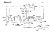
- Figure 2b illustrates a diagram of an analogue to digital converter (ADC) 200 with elements in common with the ADC illustrated in figures 1 and 2a . Similar elements between figures have been provided with similar reference numerals, and common elements discussed in relation to figure 2a will not be discussed again in detail in relation to figure 2b .
- ADC analogue to digital converter
- the ADC 200 of figure 2b builds on that shown in figure 2a , and comprises a first digital sigma delta modulator block 260 having a first digital modulator input 262 and a first digital modulator output 264.
- the first digital modulator input 262 is connected to the counter output 230 and the first digital modulator output 264 is connected to the main feedback converter input 234.
- the ADC 200 also comprises a second digital sigma delta modulator block 266 having a second digital modulator input 268 and a second digital modulator output 270.
- the second digital modulator input 268 is connected to the counter output 230 and the second digital modulator output 270 is connected to the output terminal 204.
- the first digital sigma delta modulator block 260 is a third order sigma delta modulator, while the second digital sigma delta modulator block 266 is a fifth order sigma delta modulator.
- the first digital sigma delta modulator block 260 is therefore of a lower order than the second digital sigma delta modulator block 266.
- the quantizer 220, multi-bit up/down counter 226 and third order digital SDM 238 may together be considered to be an M-bit servo and third order digital SDM 290.
- the first digital sigma delta modulator block 260 may apply a sampling frequency that is higher than the sampling frequency applied by the second digital sigma delta modulator block 266.
- a second higher order digital SDM block 266 may be used in addition to the first digital SDM block 260.
- the second higher order digital SDM block 266 may be run at a lower oversampling ratio than the first digital SDM block 260.
- the first digital SDM block 260 may operate at an oversampling frequency of 512 times the sampling frequency (512 * fs), while the second higher order digital SDM block 266 may operate at an oversampling frequency of 64, 128, 256 or 512 times the sampling frequency (64, 128, 256 or 512 * fs).
- the loop between the first digital modulator output 264 and the subtracting input 210 of the main summer 206 may be run at a high oversampling ratio, for dynamic range and slewrate requirements discussed in relation to figure 2a , while the output oversampling ratio from the second digital modulator output 270 of the second higher order digital SDM block 266 can still be at a lower oversampling ratio (such as 64 times the sample frequency (64 * fs)).
- a decimator may be connected to the output of the ADC 200 and configured to reduce the sample rate back to the sampling frequency (fs).
- any components that are described herein as being “coupled” or “connected” could be directly or indirectly coupled or connected. That is, one or more components could be located between two components that are said to be coupled or connected whilst still enabling the required functionality to be achieved.
Landscapes
- Engineering & Computer Science (AREA)
- Theoretical Computer Science (AREA)
- Compression, Expansion, Code Conversion, And Decoders (AREA)
Priority Applications (3)
| Application Number | Priority Date | Filing Date | Title |
|---|---|---|---|
| EP13187912.4A EP2860875B1 (fr) | 2013-10-09 | 2013-10-09 | Convertisseur analogique-numérique |
| US14/473,486 US9048861B2 (en) | 2013-10-09 | 2014-08-29 | Analogue to digital converter |
| CN201410528327.6A CN104579346B (zh) | 2013-10-09 | 2014-10-09 | 模数转换器 |
Applications Claiming Priority (1)
| Application Number | Priority Date | Filing Date | Title |
|---|---|---|---|
| EP13187912.4A EP2860875B1 (fr) | 2013-10-09 | 2013-10-09 | Convertisseur analogique-numérique |
Publications (2)
| Publication Number | Publication Date |
|---|---|
| EP2860875A1 true EP2860875A1 (fr) | 2015-04-15 |
| EP2860875B1 EP2860875B1 (fr) | 2019-04-10 |
Family
ID=49303896
Family Applications (1)
| Application Number | Title | Priority Date | Filing Date |
|---|---|---|---|
| EP13187912.4A Active EP2860875B1 (fr) | 2013-10-09 | 2013-10-09 | Convertisseur analogique-numérique |
Country Status (3)
| Country | Link |
|---|---|
| US (1) | US9048861B2 (fr) |
| EP (1) | EP2860875B1 (fr) |
| CN (1) | CN104579346B (fr) |
Cited By (1)
| Publication number | Priority date | Publication date | Assignee | Title |
|---|---|---|---|---|
| DE102016101741B3 (de) * | 2016-02-01 | 2017-07-13 | Infineon Technologies Ag | Hybride digitale/analoge Rauschformung bei der Sigma-Delta-Wandlung |
Families Citing this family (14)
| Publication number | Priority date | Publication date | Assignee | Title |
|---|---|---|---|---|
| US9747789B2 (en) | 2013-03-31 | 2017-08-29 | Case Western Reserve University | Magnetic resonance imaging with switched-mode current-source amplifier having gallium nitride field effect transistors for parallel transmission in MRI |
| US9397692B1 (en) * | 2015-07-16 | 2016-07-19 | Cirrus Logic International Semiconductor Ltd. | Voltage-controlled oscillator (VCO) as first stage in an analog-to-digital converter (ADC) in combination with a digital filter for second or higher-order noise shaping |
| CN105978567B (zh) * | 2016-05-04 | 2019-04-19 | 哈尔滨工程大学 | 一种具有滤波和模拟/数字转换功能的电路 |
| CN106130556B (zh) * | 2016-07-12 | 2019-10-01 | 昆明物理研究所 | 一种两步式增量模拟-数字转换器及两步式转换方法 |
| CN113037308B (zh) | 2016-10-25 | 2022-10-11 | 华为技术有限公司 | 接收机 |
| CN109995360B (zh) * | 2018-01-02 | 2023-04-14 | 珠海全志科技股份有限公司 | 抑制扰动的锁相环 |
| EP3565124A1 (fr) * | 2018-05-03 | 2019-11-06 | ams AG | Modulateur delta-sigma avec contrôle de gain automatique dans la boucle de rétroaction |
| CN112335263B (zh) | 2018-06-19 | 2022-03-18 | 美商楼氏电子有限公司 | 集成电路、麦克风组件和传感器系统 |
| DE112019003110T5 (de) * | 2018-06-19 | 2021-03-04 | Knowles Electronics, Llc | Mikrofonanordnung mit reduziertem Rauschen |
| CN112491417B (zh) * | 2019-09-12 | 2024-12-27 | 瑞昱半导体股份有限公司 | 模拟数字转换器 |
| US20210376844A1 (en) * | 2020-06-02 | 2021-12-02 | Short Circuit Technologies Llc | Event Driven Quasi-Level Crossing Delta Modulator Analog To Digital Converter With Adaptive Resolution |
| US11901919B2 (en) | 2021-04-26 | 2024-02-13 | Stmicroelectronics International N.V. | On chip test architecture for continuous time delta sigma analog-to-digital converter |
| CN114679182A (zh) * | 2022-04-20 | 2022-06-28 | 中国科学院半导体研究所 | Σ-δ型模数转换器 |
| CN117879615A (zh) * | 2023-12-05 | 2024-04-12 | 北京大学深圳研究生院 | 模数转换器及其处理方法、设备、介质 |
Citations (1)
| Publication number | Priority date | Publication date | Assignee | Title |
|---|---|---|---|---|
| EP2421156A2 (fr) * | 2010-08-16 | 2012-02-22 | NXP Semiconductors B.V. | Modulateur sigma-delta à plage dynamique étendue et faible puissance |
Family Cites Families (6)
| Publication number | Priority date | Publication date | Assignee | Title |
|---|---|---|---|---|
| JP3407871B2 (ja) * | 1999-09-17 | 2003-05-19 | 日本電気株式会社 | アナログデジタル混在δς変調器 |
| US7212137B2 (en) * | 2003-10-09 | 2007-05-01 | Cirrus Logic, Inc. | Delta sigma modulator with integral decimation |
| US7696913B2 (en) * | 2007-05-02 | 2010-04-13 | Cirrus Logic, Inc. | Signal processing system using delta-sigma modulation having an internal stabilizer path with direct output-to-integrator connection |
| US7623053B2 (en) * | 2007-09-26 | 2009-11-24 | Medtronic, Inc. | Implantable medical device with low power delta-sigma analog-to-digital converter |
| EP2410659B1 (fr) * | 2007-12-19 | 2013-11-13 | ST-Ericsson SA | Modulateur sigma-delta multibit doté d'un nombre réduit de bits dans la chaîne de réaction |
| WO2009090518A1 (fr) * | 2008-01-14 | 2009-07-23 | Nxp B.V. | Modulateur sigma-delta multibits avec un nombre de bits réduit dans la chaîne de réaction |
-
2013
- 2013-10-09 EP EP13187912.4A patent/EP2860875B1/fr active Active
-
2014
- 2014-08-29 US US14/473,486 patent/US9048861B2/en active Active
- 2014-10-09 CN CN201410528327.6A patent/CN104579346B/zh active Active
Patent Citations (1)
| Publication number | Priority date | Publication date | Assignee | Title |
|---|---|---|---|---|
| EP2421156A2 (fr) * | 2010-08-16 | 2012-02-22 | NXP Semiconductors B.V. | Modulateur sigma-delta à plage dynamique étendue et faible puissance |
Non-Patent Citations (2)
| Title |
|---|
| DÖRRER L ET AL: "A 3mW 74dB SNR 2MHz Continuous-Time Delta-Sigma ADC with a Tracking ADC Quantizer in 0.13.mu.m CMOS", IEEE JOURNAL OF SOLID-STATE CIRCUITS, IEEE SERVICE CENTER, PISCATAWAY, NJ, USA, vol. 40, no. 12, December 2005 (2005-12-01), pages 2416 - 2426, XP002440494, ISSN: 0018-9200, DOI: 10.1109/JSSC.2005.856282 * |
| ROCHA D ET AL: "ARCHITECTURES FOR A/D CONVERSION WITH OPTIMAL USE OF OVERSAMPLING", 1996 IEEE INTERNATIONAL SYMPOSIUM ON CIRCUITS AND SYSTEMS (ISCAS). CIRCUITS AND SYSTEMS CONNECTING THE WORLD. ATLANTA, MAY 12 - 15, 1996; [IEEE INTERNATIONAL SYMPOSIUM ON CIRCUITS AND SYSTEMS (ISCAS)], NEW YORK, IEEE, US, 12 May 1996 (1996-05-12), pages 37 - 40, XP000825509, ISBN: 978-0-7803-3074-0, DOI: 10.1109/ISCAS.1996.539802 * |
Cited By (2)
| Publication number | Priority date | Publication date | Assignee | Title |
|---|---|---|---|---|
| DE102016101741B3 (de) * | 2016-02-01 | 2017-07-13 | Infineon Technologies Ag | Hybride digitale/analoge Rauschformung bei der Sigma-Delta-Wandlung |
| US9871533B2 (en) | 2016-02-01 | 2018-01-16 | Infineon Technologies Ag | Hybrid digital/analog noise shaping in the sigma-delta conversion |
Also Published As
| Publication number | Publication date |
|---|---|
| CN104579346B (zh) | 2018-04-10 |
| US9048861B2 (en) | 2015-06-02 |
| EP2860875B1 (fr) | 2019-04-10 |
| US20150097711A1 (en) | 2015-04-09 |
| CN104579346A (zh) | 2015-04-29 |
Similar Documents
| Publication | Publication Date | Title |
|---|---|---|
| US9048861B2 (en) | Analogue to digital converter | |
| US9923574B2 (en) | Analogue-to-digital converter | |
| JP4890503B2 (ja) | デルタシグマ変調器 | |
| US8953813B2 (en) | Reduced delay digital active noise cancellation | |
| US9240801B2 (en) | Analog-to-digital converter | |
| KR101248563B1 (ko) | 아날로그-디지털 변환을 위한 시그마-델타 변환기들 및 방법들 | |
| KR102514329B1 (ko) | 보간을 이용하는 디지털 실리콘 마이크로폰 | |
| TW201301776A (zh) | 轉換器系統、過採樣連續時鐘轉換器及其轉換方法 | |
| US7952506B2 (en) | ΔΣ-type A/D converter | |
| US20140177874A1 (en) | Digital Microphone With Frequency Booster | |
| JP2010171484A (ja) | 半導体集積回路装置 | |
| US8384573B2 (en) | Low-power digital-to-analog converter | |
| US20070018865A1 (en) | Third order sigma-delta modulator | |
| US8963755B2 (en) | Multi-level sigma-delta ADC with reduced quantization levels | |
| CN108737944B (zh) | 用于传感器的西格玛德尔塔调制器 | |
| CN111697971A (zh) | Δ-σ模数转换器以及用于操作δ-σ模数转换器的方法 | |
| Grassi et al. | A multi-mode SC audio ΣΔ modulator for MEMS microphones with reconfigurable power consumption, noise-shaping order, and DR | |
| US9769550B2 (en) | Efficient digital microphone receiver process and system | |
| WO2013053659A1 (fr) | Convertisseur analogique-numérique (adc) sigma-delta à plusieurs niveaux présentant des niveaux de quantification réduits | |
| Lai et al. | Integrated Delta-Sigma Modulator with Low Pass Filter for Acoustical Applications | |
| Cho et al. | Design of a Stereo Audio Sigma Delta ADC with 92.4 dB SNR and-88.3 dB THD+ N | |
| Shun et al. | A multirate low power sigma delta modulator for multi-standard mobile terminals | |
| KR20080064378A (ko) | 시그마-델타 펄스 폭 변조기 및 시그마-델타 변조기 | |
| Tayyab et al. | Design of Delta Sigma Analog to Digital Converter for high fidelity MEMS microphone |
Legal Events
| Date | Code | Title | Description |
|---|---|---|---|
| PUAI | Public reference made under article 153(3) epc to a published international application that has entered the european phase |
Free format text: ORIGINAL CODE: 0009012 |
|
| 17P | Request for examination filed |
Effective date: 20140326 |
|
| AK | Designated contracting states |
Kind code of ref document: A1 Designated state(s): AL AT BE BG CH CY CZ DE DK EE ES FI FR GB GR HR HU IE IS IT LI LT LU LV MC MK MT NL NO PL PT RO RS SE SI SK SM TR |
|
| AX | Request for extension of the european patent |
Extension state: BA ME |
|
| RBV | Designated contracting states (corrected) |
Designated state(s): AL AT BE BG CH CY CZ DE DK EE ES FI FR GB GR HR HU IE IS IT LI LT LU LV MC MK MT NL NO PL PT RO RS SE SI SK SM TR |
|
| GRAP | Despatch of communication of intention to grant a patent |
Free format text: ORIGINAL CODE: EPIDOSNIGR1 |
|
| STAA | Information on the status of an ep patent application or granted ep patent |
Free format text: STATUS: GRANT OF PATENT IS INTENDED |
|
| INTG | Intention to grant announced |
Effective date: 20180830 |
|
| GRAJ | Information related to disapproval of communication of intention to grant by the applicant or resumption of examination proceedings by the epo deleted |
Free format text: ORIGINAL CODE: EPIDOSDIGR1 |
|
| STAA | Information on the status of an ep patent application or granted ep patent |
Free format text: STATUS: REQUEST FOR EXAMINATION WAS MADE |
|
| INTC | Intention to grant announced (deleted) | ||
| GRAP | Despatch of communication of intention to grant a patent |
Free format text: ORIGINAL CODE: EPIDOSNIGR1 |
|
| STAA | Information on the status of an ep patent application or granted ep patent |
Free format text: STATUS: GRANT OF PATENT IS INTENDED |
|
| GRAS | Grant fee paid |
Free format text: ORIGINAL CODE: EPIDOSNIGR3 |
|
| GRAA | (expected) grant |
Free format text: ORIGINAL CODE: 0009210 |
|
| STAA | Information on the status of an ep patent application or granted ep patent |
Free format text: STATUS: THE PATENT HAS BEEN GRANTED |
|
| INTG | Intention to grant announced |
Effective date: 20190215 |
|
| AK | Designated contracting states |
Kind code of ref document: B1 Designated state(s): AL AT BE BG CH CY CZ DE DK EE ES FI FR GB GR HR HU IE IS IT LI LT LU LV MC MK MT NL NO PL PT RO RS SE SI SK SM TR |
|
| REG | Reference to a national code |
Ref country code: GB Ref legal event code: FG4D |
|
| REG | Reference to a national code |
Ref country code: CH Ref legal event code: EP Ref country code: AT Ref legal event code: REF Ref document number: 1120068 Country of ref document: AT Kind code of ref document: T Effective date: 20190415 |
|
| REG | Reference to a national code |
Ref country code: IE Ref legal event code: FG4D |
|
| REG | Reference to a national code |
Ref country code: DE Ref legal event code: R096 Ref document number: 602013053586 Country of ref document: DE |
|
| REG | Reference to a national code |
Ref country code: NL Ref legal event code: MP Effective date: 20190410 |
|
| REG | Reference to a national code |
Ref country code: LT Ref legal event code: MG4D |
|
| REG | Reference to a national code |
Ref country code: AT Ref legal event code: MK05 Ref document number: 1120068 Country of ref document: AT Kind code of ref document: T Effective date: 20190410 |
|
| PG25 | Lapsed in a contracting state [announced via postgrant information from national office to epo] |
Ref country code: NL Free format text: LAPSE BECAUSE OF FAILURE TO SUBMIT A TRANSLATION OF THE DESCRIPTION OR TO PAY THE FEE WITHIN THE PRESCRIBED TIME-LIMIT Effective date: 20190410 |
|
| PG25 | Lapsed in a contracting state [announced via postgrant information from national office to epo] |
Ref country code: FI Free format text: LAPSE BECAUSE OF FAILURE TO SUBMIT A TRANSLATION OF THE DESCRIPTION OR TO PAY THE FEE WITHIN THE PRESCRIBED TIME-LIMIT Effective date: 20190410 Ref country code: PT Free format text: LAPSE BECAUSE OF FAILURE TO SUBMIT A TRANSLATION OF THE DESCRIPTION OR TO PAY THE FEE WITHIN THE PRESCRIBED TIME-LIMIT Effective date: 20190910 Ref country code: NO Free format text: LAPSE BECAUSE OF FAILURE TO SUBMIT A TRANSLATION OF THE DESCRIPTION OR TO PAY THE FEE WITHIN THE PRESCRIBED TIME-LIMIT Effective date: 20190710 Ref country code: ES Free format text: LAPSE BECAUSE OF FAILURE TO SUBMIT A TRANSLATION OF THE DESCRIPTION OR TO PAY THE FEE WITHIN THE PRESCRIBED TIME-LIMIT Effective date: 20190410 Ref country code: AL Free format text: LAPSE BECAUSE OF FAILURE TO SUBMIT A TRANSLATION OF THE DESCRIPTION OR TO PAY THE FEE WITHIN THE PRESCRIBED TIME-LIMIT Effective date: 20190410 Ref country code: SE Free format text: LAPSE BECAUSE OF FAILURE TO SUBMIT A TRANSLATION OF THE DESCRIPTION OR TO PAY THE FEE WITHIN THE PRESCRIBED TIME-LIMIT Effective date: 20190410 Ref country code: HR Free format text: LAPSE BECAUSE OF FAILURE TO SUBMIT A TRANSLATION OF THE DESCRIPTION OR TO PAY THE FEE WITHIN THE PRESCRIBED TIME-LIMIT Effective date: 20190410 Ref country code: LT Free format text: LAPSE BECAUSE OF FAILURE TO SUBMIT A TRANSLATION OF THE DESCRIPTION OR TO PAY THE FEE WITHIN THE PRESCRIBED TIME-LIMIT Effective date: 20190410 |
|
| PG25 | Lapsed in a contracting state [announced via postgrant information from national office to epo] |
Ref country code: PL Free format text: LAPSE BECAUSE OF FAILURE TO SUBMIT A TRANSLATION OF THE DESCRIPTION OR TO PAY THE FEE WITHIN THE PRESCRIBED TIME-LIMIT Effective date: 20190410 Ref country code: RS Free format text: LAPSE BECAUSE OF FAILURE TO SUBMIT A TRANSLATION OF THE DESCRIPTION OR TO PAY THE FEE WITHIN THE PRESCRIBED TIME-LIMIT Effective date: 20190410 Ref country code: BG Free format text: LAPSE BECAUSE OF FAILURE TO SUBMIT A TRANSLATION OF THE DESCRIPTION OR TO PAY THE FEE WITHIN THE PRESCRIBED TIME-LIMIT Effective date: 20190710 Ref country code: GR Free format text: LAPSE BECAUSE OF FAILURE TO SUBMIT A TRANSLATION OF THE DESCRIPTION OR TO PAY THE FEE WITHIN THE PRESCRIBED TIME-LIMIT Effective date: 20190711 Ref country code: LV Free format text: LAPSE BECAUSE OF FAILURE TO SUBMIT A TRANSLATION OF THE DESCRIPTION OR TO PAY THE FEE WITHIN THE PRESCRIBED TIME-LIMIT Effective date: 20190410 |
|
| PG25 | Lapsed in a contracting state [announced via postgrant information from national office to epo] |
Ref country code: AT Free format text: LAPSE BECAUSE OF FAILURE TO SUBMIT A TRANSLATION OF THE DESCRIPTION OR TO PAY THE FEE WITHIN THE PRESCRIBED TIME-LIMIT Effective date: 20190410 Ref country code: IS Free format text: LAPSE BECAUSE OF FAILURE TO SUBMIT A TRANSLATION OF THE DESCRIPTION OR TO PAY THE FEE WITHIN THE PRESCRIBED TIME-LIMIT Effective date: 20190810 |
|
| REG | Reference to a national code |
Ref country code: DE Ref legal event code: R097 Ref document number: 602013053586 Country of ref document: DE |
|
| PG25 | Lapsed in a contracting state [announced via postgrant information from national office to epo] |
Ref country code: RO Free format text: LAPSE BECAUSE OF FAILURE TO SUBMIT A TRANSLATION OF THE DESCRIPTION OR TO PAY THE FEE WITHIN THE PRESCRIBED TIME-LIMIT Effective date: 20190410 Ref country code: SK Free format text: LAPSE BECAUSE OF FAILURE TO SUBMIT A TRANSLATION OF THE DESCRIPTION OR TO PAY THE FEE WITHIN THE PRESCRIBED TIME-LIMIT Effective date: 20190410 Ref country code: CZ Free format text: LAPSE BECAUSE OF FAILURE TO SUBMIT A TRANSLATION OF THE DESCRIPTION OR TO PAY THE FEE WITHIN THE PRESCRIBED TIME-LIMIT Effective date: 20190410 Ref country code: EE Free format text: LAPSE BECAUSE OF FAILURE TO SUBMIT A TRANSLATION OF THE DESCRIPTION OR TO PAY THE FEE WITHIN THE PRESCRIBED TIME-LIMIT Effective date: 20190410 Ref country code: DK Free format text: LAPSE BECAUSE OF FAILURE TO SUBMIT A TRANSLATION OF THE DESCRIPTION OR TO PAY THE FEE WITHIN THE PRESCRIBED TIME-LIMIT Effective date: 20190410 |
|
| PLBE | No opposition filed within time limit |
Free format text: ORIGINAL CODE: 0009261 |
|
| STAA | Information on the status of an ep patent application or granted ep patent |
Free format text: STATUS: NO OPPOSITION FILED WITHIN TIME LIMIT |
|
| PG25 | Lapsed in a contracting state [announced via postgrant information from national office to epo] |
Ref country code: IT Free format text: LAPSE BECAUSE OF FAILURE TO SUBMIT A TRANSLATION OF THE DESCRIPTION OR TO PAY THE FEE WITHIN THE PRESCRIBED TIME-LIMIT Effective date: 20190410 Ref country code: SM Free format text: LAPSE BECAUSE OF FAILURE TO SUBMIT A TRANSLATION OF THE DESCRIPTION OR TO PAY THE FEE WITHIN THE PRESCRIBED TIME-LIMIT Effective date: 20190410 |
|
| 26N | No opposition filed |
Effective date: 20200113 |
|
| PG25 | Lapsed in a contracting state [announced via postgrant information from national office to epo] |
Ref country code: TR Free format text: LAPSE BECAUSE OF FAILURE TO SUBMIT A TRANSLATION OF THE DESCRIPTION OR TO PAY THE FEE WITHIN THE PRESCRIBED TIME-LIMIT Effective date: 20190410 |
|
| PG25 | Lapsed in a contracting state [announced via postgrant information from national office to epo] |
Ref country code: SI Free format text: LAPSE BECAUSE OF FAILURE TO SUBMIT A TRANSLATION OF THE DESCRIPTION OR TO PAY THE FEE WITHIN THE PRESCRIBED TIME-LIMIT Effective date: 20190410 Ref country code: MC Free format text: LAPSE BECAUSE OF FAILURE TO SUBMIT A TRANSLATION OF THE DESCRIPTION OR TO PAY THE FEE WITHIN THE PRESCRIBED TIME-LIMIT Effective date: 20190410 |
|
| REG | Reference to a national code |
Ref country code: CH Ref legal event code: PL |
|
| PG25 | Lapsed in a contracting state [announced via postgrant information from national office to epo] |
Ref country code: LU Free format text: LAPSE BECAUSE OF NON-PAYMENT OF DUE FEES Effective date: 20191009 Ref country code: CH Free format text: LAPSE BECAUSE OF NON-PAYMENT OF DUE FEES Effective date: 20191031 Ref country code: LI Free format text: LAPSE BECAUSE OF NON-PAYMENT OF DUE FEES Effective date: 20191031 |
|
| REG | Reference to a national code |
Ref country code: BE Ref legal event code: MM Effective date: 20191031 |
|
| PG25 | Lapsed in a contracting state [announced via postgrant information from national office to epo] |
Ref country code: BE Free format text: LAPSE BECAUSE OF NON-PAYMENT OF DUE FEES Effective date: 20191031 |
|
| GBPC | Gb: european patent ceased through non-payment of renewal fee |
Effective date: 20191009 |
|
| PG25 | Lapsed in a contracting state [announced via postgrant information from national office to epo] |
Ref country code: IE Free format text: LAPSE BECAUSE OF NON-PAYMENT OF DUE FEES Effective date: 20191009 Ref country code: GB Free format text: LAPSE BECAUSE OF NON-PAYMENT OF DUE FEES Effective date: 20191009 |
|
| PG25 | Lapsed in a contracting state [announced via postgrant information from national office to epo] |
Ref country code: CY Free format text: LAPSE BECAUSE OF FAILURE TO SUBMIT A TRANSLATION OF THE DESCRIPTION OR TO PAY THE FEE WITHIN THE PRESCRIBED TIME-LIMIT Effective date: 20190410 |
|
| PG25 | Lapsed in a contracting state [announced via postgrant information from national office to epo] |
Ref country code: HU Free format text: LAPSE BECAUSE OF FAILURE TO SUBMIT A TRANSLATION OF THE DESCRIPTION OR TO PAY THE FEE WITHIN THE PRESCRIBED TIME-LIMIT; INVALID AB INITIO Effective date: 20131009 Ref country code: MT Free format text: LAPSE BECAUSE OF FAILURE TO SUBMIT A TRANSLATION OF THE DESCRIPTION OR TO PAY THE FEE WITHIN THE PRESCRIBED TIME-LIMIT Effective date: 20190410 |
|
| PG25 | Lapsed in a contracting state [announced via postgrant information from national office to epo] |
Ref country code: MK Free format text: LAPSE BECAUSE OF FAILURE TO SUBMIT A TRANSLATION OF THE DESCRIPTION OR TO PAY THE FEE WITHIN THE PRESCRIBED TIME-LIMIT Effective date: 20190410 |
|
| P01 | Opt-out of the competence of the unified patent court (upc) registered |
Effective date: 20230725 |
|
| PGFP | Annual fee paid to national office [announced via postgrant information from national office to epo] |
Ref country code: FR Payment date: 20250924 Year of fee payment: 13 |
|
| PGFP | Annual fee paid to national office [announced via postgrant information from national office to epo] |
Ref country code: DE Payment date: 20250923 Year of fee payment: 13 |