EP2862424B1 - Verfahren zur herstellung einer elektronischen schaltung mit schutz der leitenden schicht - Google Patents
Verfahren zur herstellung einer elektronischen schaltung mit schutz der leitenden schicht Download PDFInfo
- Publication number
- EP2862424B1 EP2862424B1 EP13729015.1A EP13729015A EP2862424B1 EP 2862424 B1 EP2862424 B1 EP 2862424B1 EP 13729015 A EP13729015 A EP 13729015A EP 2862424 B1 EP2862424 B1 EP 2862424B1
- Authority
- EP
- European Patent Office
- Prior art keywords
- protective material
- bottom wall
- electronic component
- conductive layer
- layer
- Prior art date
- Legal status (The legal status is an assumption and is not a legal conclusion. Google has not performed a legal analysis and makes no representation as to the accuracy of the status listed.)
- Active
Links
Images

Classifications
-
- H—ELECTRICITY
- H05—ELECTRIC TECHNIQUES NOT OTHERWISE PROVIDED FOR
- H05K—PRINTED CIRCUITS; CASINGS OR CONSTRUCTIONAL DETAILS OF ELECTRIC APPARATUS; MANUFACTURE OF ASSEMBLAGES OF ELECTRICAL COMPONENTS
- H05K3/00—Apparatus or processes for manufacturing printed circuits
- H05K3/30—Assembling printed circuits with electric components, e.g. with resistors
- H05K3/32—Assembling printed circuits with electric components, e.g. with resistors electrically connecting electric components or wires to printed circuits
-
- H—ELECTRICITY
- H05—ELECTRIC TECHNIQUES NOT OTHERWISE PROVIDED FOR
- H05K—PRINTED CIRCUITS; CASINGS OR CONSTRUCTIONAL DETAILS OF ELECTRIC APPARATUS; MANUFACTURE OF ASSEMBLAGES OF ELECTRICAL COMPONENTS
- H05K1/00—Printed circuits
- H05K1/18—Printed circuits structurally associated with non-printed electric components
- H05K1/189—Printed circuits structurally associated with non-printed electric components characterised by the use of flexible or folded printed circuits
-
- H—ELECTRICITY
- H05—ELECTRIC TECHNIQUES NOT OTHERWISE PROVIDED FOR
- H05K—PRINTED CIRCUITS; CASINGS OR CONSTRUCTIONAL DETAILS OF ELECTRIC APPARATUS; MANUFACTURE OF ASSEMBLAGES OF ELECTRICAL COMPONENTS
- H05K3/00—Apparatus or processes for manufacturing printed circuits
- H05K3/0011—Working of insulating substrates or insulating layers
- H05K3/0017—Etching of the substrate by chemical or physical means
-
- H—ELECTRICITY
- H05—ELECTRIC TECHNIQUES NOT OTHERWISE PROVIDED FOR
- H05K—PRINTED CIRCUITS; CASINGS OR CONSTRUCTIONAL DETAILS OF ELECTRIC APPARATUS; MANUFACTURE OF ASSEMBLAGES OF ELECTRICAL COMPONENTS
- H05K3/00—Apparatus or processes for manufacturing printed circuits
- H05K3/0011—Working of insulating substrates or insulating layers
- H05K3/0017—Etching of the substrate by chemical or physical means
- H05K3/002—Etching of the substrate by chemical or physical means by liquid chemical etching
-
- H—ELECTRICITY
- H05—ELECTRIC TECHNIQUES NOT OTHERWISE PROVIDED FOR
- H05K—PRINTED CIRCUITS; CASINGS OR CONSTRUCTIONAL DETAILS OF ELECTRIC APPARATUS; MANUFACTURE OF ASSEMBLAGES OF ELECTRICAL COMPONENTS
- H05K3/00—Apparatus or processes for manufacturing printed circuits
- H05K3/02—Apparatus or processes for manufacturing printed circuits in which the conductive material is applied to the surface of the insulating support and is thereafter removed from such areas of the surface which are not intended for current conducting or shielding
- H05K3/06—Apparatus or processes for manufacturing printed circuits in which the conductive material is applied to the surface of the insulating support and is thereafter removed from such areas of the surface which are not intended for current conducting or shielding the conductive material being removed chemically or electrolytically, e.g. by photo-etch process
-
- H—ELECTRICITY
- H05—ELECTRIC TECHNIQUES NOT OTHERWISE PROVIDED FOR
- H05K—PRINTED CIRCUITS; CASINGS OR CONSTRUCTIONAL DETAILS OF ELECTRIC APPARATUS; MANUFACTURE OF ASSEMBLAGES OF ELECTRICAL COMPONENTS
- H05K2201/00—Indexing scheme relating to printed circuits covered by H05K1/00
- H05K2201/03—Conductive materials
- H05K2201/0332—Structure of the conductor
- H05K2201/0388—Other aspects of conductors
- H05K2201/0397—Tab
-
- H—ELECTRICITY
- H05—ELECTRIC TECHNIQUES NOT OTHERWISE PROVIDED FOR
- H05K—PRINTED CIRCUITS; CASINGS OR CONSTRUCTIONAL DETAILS OF ELECTRIC APPARATUS; MANUFACTURE OF ASSEMBLAGES OF ELECTRICAL COMPONENTS
- H05K2201/00—Indexing scheme relating to printed circuits covered by H05K1/00
- H05K2201/10—Details of components or other objects attached to or integrated in a printed circuit board
- H05K2201/10007—Types of components
- H05K2201/10106—Light emitting diode [LED]
-
- H—ELECTRICITY
- H05—ELECTRIC TECHNIQUES NOT OTHERWISE PROVIDED FOR
- H05K—PRINTED CIRCUITS; CASINGS OR CONSTRUCTIONAL DETAILS OF ELECTRIC APPARATUS; MANUFACTURE OF ASSEMBLAGES OF ELECTRICAL COMPONENTS
- H05K3/00—Apparatus or processes for manufacturing printed circuits
- H05K3/40—Forming printed elements for providing electric connections to or between printed circuits
- H05K3/4092—Integral conductive tabs, i.e. conductive parts partly detached from the substrate
-
- Y—GENERAL TAGGING OF NEW TECHNOLOGICAL DEVELOPMENTS; GENERAL TAGGING OF CROSS-SECTIONAL TECHNOLOGIES SPANNING OVER SEVERAL SECTIONS OF THE IPC; TECHNICAL SUBJECTS COVERED BY FORMER USPC CROSS-REFERENCE ART COLLECTIONS [XRACs] AND DIGESTS
- Y10—TECHNICAL SUBJECTS COVERED BY FORMER USPC
- Y10T—TECHNICAL SUBJECTS COVERED BY FORMER US CLASSIFICATION
- Y10T29/00—Metal working
- Y10T29/49—Method of mechanical manufacture
- Y10T29/49002—Electrical device making
- Y10T29/49117—Conductor or circuit manufacturing
- Y10T29/49124—On flat or curved insulated base, e.g., printed circuit, etc.
- Y10T29/4913—Assembling to base an electrical component, e.g., capacitor, etc.
- Y10T29/49133—Assembling to base an electrical component, e.g., capacitor, etc. with component orienting
Definitions
- the invention relates to the production of electronic circuits, in particular printed circuits.
- the invention also relates to the production of electronic circuits, in particular printed circuits, carrying one or more components which components have contacts on one side and where these contacts are intended to be electrically connected to conductive tracks of the circuit for contacting such leads. by respective intermediate wire links extending from the contact to the conductive track, or wire-bonding components according to the English terminology.
- the invention relates in particular to the production of such flexible type electronic circuits.
- the invention particularly relates to the realization of such circuits when the components are light emitting components such as light emitting diodes - or LEDs for Light Emitting Diode in English -
- a support consisting in particular of a dielectric film and a copper foil laminated together.
- the dielectric film is pre-perforated before rolling to include a number of windows for each receiving one or more components so that the component or components are placed at the bottom of a cavity defined by the window of the dielectric film.
- US3480836 discloses such an arrangement.
- Such a circuit it is also necessary to provide grooves in the copper layer and in particular in a portion of the copper layer which forms the bottom of the cavity. Such grooves serve to separate electrically different ranges of the bottom of the cavity, such as a range connected to a contact forming the anode of the component and a range connected to a contact forming the cathode of the component. Such furrows at the bottom of the cavity also serve to delimit electrical tracks connecting different members of the circuit such as the component placed in the cavity or other components of the circuit.
- a circuit manufacturing method comprising a support which support comprises a conductive layer and a dielectric film laminated between them, the method including a step of making windows in the dielectric film so that the support forms cavities having a bottom wall formed by the conductive layer and edges formed by the dielectric film, the method including the step of placing against the bottom wall of a cavity and connect to the bottom wall an electronic component, the method comprising the step of engraving grooves in the conductive layer, this etching step of the conductive layer being performed after the rolling of the the conductive layer with the dielectric film using an etching solution and the method comprising a preliminary step in the etching step, which preliminary step consists in depositing a layer of protective material on the conductive layer in the bottom of the cavity and on at least a portion of the dielectric film forming the edges of the cavity, which maté Protection element is a liquid material capable of hardening and resisting once cured to the etching solution implemented during the step of etching the conductive layer.
- the step of placing an electronic component against the bottom wall of a cavity and connecting the electronic component to the bottom wall comprises connecting the electronic component to the bottom wall without a wired connection. intermediate.
- the step of placing an electronic component against the bottom wall of a cavity and connecting the electronic component to the bottom wall comprises connecting the electronic component to the bottom wall by a wire link which extends from the electronic component to the bottom wall.
- the electronic component is an electroluminescent component.
- the protective material is an ink.
- the protective material is a resin.
- the protective material is a mixture of at least one ink and at least one resin.
- the protective material is part of the group consisting of mono or bi-component polyurethanes, acrylic or methacrylic resins, ultraviolet-crosslinkable acrylic resins, styrene maleic anhydride copolymers, acrylic styrene copolymers, methacrylic acrylic copolymers, phenol formaldehyde resins, novolac resins, epoxy resins.
- the protective material is a material which can be cured by exposure to light and the method comprises the step of exposing the protective material to light to cure it.
- the method comprises a step subsequent to the etching step which consists in removing the layer of protective material.
- the step of removing the layer of protective material consists of immersing the support in a bath of etching solution of the layer of protective material.
- the protective material is applied by an operation forming part of the group consisting of a spraying, a coating, an impression.
- the circuit is a flexible type circuit.
- an electronic circuit support 1 is constituted by a copper foil 10 and a dielectric film 20 laminated between them.
- the dielectric film 20 and the copper foil are of sufficiently low thickness that the carrier 1 is of flexible type.
- the dielectric film 20 and the copper foil are before rolling in the form of rolls and will now be described different processing steps which will preferably be performed by unwinding and winding a roll of such a sheet, film or support, thus allowing a particularly high speed of implementation of the process which will be described now.
- the dielectric film 20 is here an epoxy glass film, which has undergone a sizing step on an upper face and then a perforation step before being laminated with the copper layer 10.
- the perforations here form two windows 21, 22 in the film 20 to each receive a component which will be described later and which will be in the present example a luminescent component.
- the windows here represented two in number for the sake of simplicity of the disclosure, are preferentially homogeneously distributed for an equally homogeneous distribution of light released by the luminescent components.
- the luminescent component is a bare-chip or bare-chip semiconductor component.
- Such a naked chip is also called dice or "dice” in English, by the industrial process typically used to obtain such a naked chip.
- Such a method consists in producing large batches of the same integrated circuit which consists of diffusion trace elements having a selected configuration on a surface of a substrate or "wafer” in English. The wafer is then cut into small pieces each forming a copy of the circuit. Each of these pieces is therefore a "dice” or “dice” in English.
- the bare chip or bare chip consists of a substrate on which is deposited a succession of semiconductor layers, which succession of semiconductor layers has the ability to emit light when a potential difference is applied. between two specific layers of this succession of layers.
- Such a bare chip typically has a width of a few tens of micrometers and such a bare chip has contact pads of a width of a few tens of micrometers, typically between 50 and 100 micrometers.
- the present naked chip is here a flipped chip or chip "flip chip” according to the English terminology, which includes contact pads on one side of the chip to be positioned vis-à-vis the tracks of a circuit so that the chip is put in connection with these conductive tracks without intermediate wired connection, typically via a solder paste.
- the bare chip is connected to the tracks of the circuit by wired links which extend each time from a contact of the chip and up to a corresponding track of the circuit, according to the technology known under the name wire bonding according to the English terminology, the wire links being for example soldered to the tracks of the circuit.
- the luminescent component is a surface mount component or SMC for Surface Mount Component according to the English designation.
- SMT Surface Mount Technology
- SMCs surface mount components
- SMD Surface Mounted Device
- An SMC comprises a substrate and a bare chip similar to that described above.
- the bare chip is fixed on a first face of the substrate, and the substrate has conductive pads on a second face of the substrate.
- the conductive pads of the bare chip are connected to the conductive pads of the substrate by means of wire bonds.
- An encapsulation body is overmolded on the bare chip and on the wire links so that the SMC forms a protected and robust component that can be easily and directly mounted on a support provided with conductive tracks.
- An SMC has a size typically of the order of half a millimeter.
- the conductive pads of an SMC have a size typically of the order of a few hundred micrometers. We use here such a SMC that is flip chip type or flipped in French, so that the SMC is placed in a window 21, 22 with its contact pads placed vis-à-vis conductive tracks formed by the layer of copper 10 and connected thereto without an intermediate wire link.
- the SMC is placed in the cavity and connected to the conductive tracks constituted by the copper layer 10 via wire links.
- the SMC is advantageously placed so that its contacts are directed in a direction away from the copper layer 10.
- the wire links are advantageously welded to both the contacts of the SMC and to the conductive tracks constituted by the copper layer 10.
- Such grooves are here made by chemical etching of the copper layer, here using a chemical etching reagent known per se based on cupric chloride and comprising hydrochloric acid.
- Each cavity 21, 22 has a respective bottom wall 11, 12 constituted by a portion of the copper layer 10 which is not supported by any substrate, which portion of the copper layer forming the bottom wall is thus bare on both its sides. faces and exposed in this state to an attack of the chemical etching solution.
- the copper layer 10 Before being immersed in a bath of such an etching reagent, the copper layer 10 will be protected on its face located on the side opposite to that carrying the dielectric film 20, in its areas complementary to those to be etched. Such protection will be achieved by deposition, exposure, development and cleaning of a photosensitive protection film.
- a liquid layer 30 which here consists of a hardening and resistant ink, once cured, the etching reagent used later to engrave the grooves.
- Such ink resistant to etching or ink etch resist in English has the advantage, because of its liquid form, to come to marry more easily any form of wall and thus to ensure here the filling cavities to protect.
- Such ink etch resist may be a photosensitive ink or not.
- the ink used is preferably removable or "strippable" in English by using a specific attack solution or “stripping” in English acting on such ink.
- the ink used is thus preferentially “strippable” in alkaline or solvent medium.
- liquid ink such as a coating for example by roll, to the curtain, or using a slot-type nozzle or "slot die" in English terminology .
- the ink can be applied by printing, for example by screen printing, by ink jet, or by "offset" technique according to the English-speaking terminology, etc.
- the method of applying the ink is chosen according to the characteristics and the viscosity of the ink used.
- the protective material applied in liquid form and resistant to chemical etching once cured may be a resin, or a mixture of ink and resin.
- a protective layer may thus be chosen to be curable by exposure to light or not.
- Suitable chemical families are mono or bicomponent polyurethanes, acrylic or methacrylic resins which may be hydroxylated or carboxylated, ultraviolet crosslinkable acrylic resins, styrene maleic anhydride copolymers, acrylic styrene copolymers, methacrylic acrylic copolymers, phenol formaldehyde resins, novolac resins or phenol formaldehyde resins, etc.
- Such inks or resins are available on the market, for example under the references and brands of Atotech's APR-68, Huntsman's Probimage 120, Coates' XV750 Imageline Etch Resist Family, Photoposit SN68H, SP 24 of the Rohm and Haas Company, AS500-LY from Taiyo Ink Company, ETP 240RC, ETAV 24 from Electra Polymers Ltd, ELPEMER RC2054 HR from Peters SMA1440F resin from Arkema, Joncryl 678 from BASF, Alnovol PN 160 from Cytec, etc.
- the stripping can be carried out with an aqueous alkaline solution, for example a 2% solution of sodium hydroxide or potassium hydroxide or a solvent of the family of ketones, esters or alcohols such as acetone, methyl ethyl ketone, ethyl acetate, ethanol, etc.
- an aqueous alkaline solution for example a 2% solution of sodium hydroxide or potassium hydroxide or a solvent of the family of ketones, esters or alcohols such as acetone, methyl ethyl ketone, ethyl acetate, ethanol, etc.
- a protective layer 40 is then formed on the face of the copper layer 10 which is arranged opposite the dielectric layer 20, according to a technique known per se of photosensitive film or photosensitive lacquer, insolation of this layer. film or lacquer according to a desired topography, development and chemical removal of non-insolated areas.
- the protective film 40 finally has the configuration shown in FIG. figure 3 , where it has openings 41 which leave exposed areas 13 of the copper layer 10 on the opposite side to that carrying the dielectric layer 20.
- the etching is then performed by immersing this assembly in the bath of etching solution.
- the solution then enters the openings 41 of the protective film 40 and digs a groove 14 in the copper layer 10, here in the central position of the cavities 21, 22.
- the etching solution passes through the copper layer 10 and then reaches the layer of protective material 30, where it is stopped so that it can not reach the opposite side of the copper layer 10 forming the bottom of the cavity considered 21, 22.
- the face of the copper layer 10 forming the bottom of the cavity 21, 22 is thus protected from any alteration by the etching solution and remains intact for positioning, fixing and contacting the component.
- a next step consists in removing the photo-imaged protection film 40 and the layer of protective material 30, by immersion in stripping baths adapted to each of the materials constituting these layers 30 and 40.
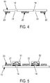
- the whole obtained, represented at figure 4 then consists of a support having a series of cavities 21,22 each provided with a central groove 14 separating two respective contact pads from the bottom of the cavity in question.
- the protective material 30 matches the bottom of the cavity formed by the copper layer 10 as well as the edges of the cavity formed by the edges of the windows of the dielectric film 20.
- the protective material 30 in particular adheres to the copper layer in an area of the bottom of the cavity 21, 22 where the groove must be made. So the use of material “Etch resist” liquid to protect the bottom of the cavity makes this technology very flexible and can adapt to many product configurations.
- the cavities have a width between 650 ⁇ m and 2.8mm
- the process is adaptable to much larger cavities or much narrower.
- the method is also adaptable to variations in the shape of the cavities to be protected, such as square, rectangular, circular shapes, as well as variations in the number and / or density of the cavities to be protected and thus in the varied spaces between them. cavities.
- the spaces between adjacent cavities is for example between 1.5 mm and 9.5 mm, corresponding to a number of cavities ranging from 6 to 18 cavities for a width having a value of 70 mm.
- the method is also adapted to variations in the thickness of the dielectric film 20 and thus the depth of the cavities 21, 22 to be filled.
- the cavities 21, 22 have a thickness of 200 .mu.m.
- the method is also adapted to variations in the thickness of the copper layer 10 to be protected and therefore the parameters used in etching, the copper layer possibly being, for example, a 35 or 70 ⁇ m thick copper foil.
- the method is also adapted to variations in the shape of the groove or here the inter-track to be engraved, this groove being for example in a straight line, in "S", "T” or any other form of line.
- the assembly obtained is then subjected to a finishing layer deposition operation on the face of the support 1 where the dielectric layer 20 is located.
- a metal finishing layer thus covers both the copper layer 10 in the bottom of the layers. cavities 21, 22 and the dielectric layer 20 in its exposed parts, that is to say both in its zones extending in the main plane of the support 1 and in its zones forming the vertical edges of the cavities 21 22.
- the topcoat consists of a layer of a noble metal with a metal such as Nickel or Gold, Silver, Palladium etc., or an alloy of one or more of these metals, or a succession of layers of one or more of these metals as needed.
- This finishing layer protects the support from mechanical aggression, oxidation, and provides a reflective effect favorable to the lighting effect generated by the assembly.
- Such a final metallization is flexible: the metallization can be carried out electrolytically or without the use of electrode deposition according to a technique also called "electroless" according to the English terminology.
- soldermask material is preferably a laminated material on the face of the copper layer 10 which is opposite to that carrying the dielectric film 20 so that it causes at least partial penetration of this material in the grooves 14 made .
- the material is preferably an insolable, developable and thermally crosslinkable material for easy and precise placement of the latter.
- the components 51, 52 are positioned within the cavities 21, 22, being fixed and brought into contact with the bottom of each cavity which is formed by the copper layer 10, here via a conductive brazing paste disposed under the contact pads of these components 51, 52 or for example by gold son.
- the invention is suitable for producing circuits carrying components based on semiconductors which do not have a luminescent function but perform other functions such as example of the electrical processing functions and / or data.
Landscapes
- Engineering & Computer Science (AREA)
- Microelectronics & Electronic Packaging (AREA)
- Manufacturing & Machinery (AREA)
- Chemical & Material Sciences (AREA)
- Chemical Kinetics & Catalysis (AREA)
- General Chemical & Material Sciences (AREA)
- Manufacturing Of Printed Circuit Boards (AREA)
Claims (13)
- Verfahren zur Herstellung einer Schaltung, die einen Träger (1) enthält, wobei der Träger (1) eine leitende Schicht (10) und eine dielektrische Folie (20) enthält, die miteinander laminiert sind, wobei das Verfahren einen Schritt der Herstellung von Fenstern (21, 22) in der dielektrischen Folie (20) umfasst, damit der Träger (1) Hohlräume (21, 22) bildet, die eine aus der leitenden Schicht (10) bestehende Bodenwand und aus der dielektrischen Folie (20) bestehende Ränder haben, wobei das Verfahren den Schritt umfasst, der darin besteht, ein elektronisches Bauteil (51, 52) gegen die Bodenwand eines Hohlraums (21, 22) zu platzieren und mit der Bodenwand zu verbinden, und das Verfahren den Schritt enthält, der darin besteht, Rillen (14) in die leitende Schicht (10) zu ätzen, wobei dieser Ätzschritt der leitenden Schicht (10) nach dem Laminieren der leitenden Schicht (10) mit der dielektrischen Folie (20) mit Hilfe einer Ätzlösung durchgeführt wird, und das Verfahren einen vor dem Ätzschritt liegenden Schritt enthält, wobei der vorherige Schritt darin besteht, eine Schicht von Schutzmaterial (30) auf die leitende Schicht (10) am Boden des Hohlraums (21, 22) und auf mindestens einen Teil der die Ränder des Hohlraums (21, 22) bildenden dielektrischen Folie (20) aufzubringen, wobei das Schutzmaterial (30) ein flüssiges Material ist, das härten kann und, wenn es gehärtet ist, der Ätzlösung widersteht, die im Ätzschritt der leitenden Schicht (10) verwendet wird.
- Verfahren nach Anspruch 1, dadurch gekennzeichnet, dass der Schritt, der darin besteht, ein elektronisches Bauteil gegen die Bodenwand eines Hohlraums (21, 22) zu platzieren und das elektronische Bauteil (51, 52) mit der Bodenwand zu verbinden, die Verbindung des elektronischen Bauteils (51, 52) mit der Bodenwand ohne Zwischendrahtverbindung enthält.
- Verfahren nach Anspruch 1, dadurch gekennzeichnet, dass der Schritt, der darin besteht, ein elektronisches Bauteil gegen die Bodenwand eines Hohlraums (21, 22) zu platzieren und das elektronische Bauteil (51, 52) mit der Bodenwand zu verbinden, die Verbindung des elektronischen Bauteils (51, 52) mit der Bodenwand über eine Drahtverbindung enthält, die sich vom elektronischen Bauteil zur Bodenwand erstreckt.
- Verfahren nach einem der vorhergehenden Ansprüche, dadurch gekennzeichnet, dass das elektronische Bauteil (51, 52) ein Elektrolumineszenzbauteil ist.
- Verfahren nach einem der vorhergehenden Ansprüche, dadurch gekennzeichnet, dass das Schutzmaterial (30) eine Druckfarbe ist.
- Verfahren nach einem der Ansprüche 1 bis 4, dadurch gekennzeichnet, dass das Schutzmaterial (30) ein Harz ist.
- Verfahren nach einem der Ansprüche 1 bis 4, dadurch gekennzeichnet, dass das Schutzmaterial (30) eine Mischung aus mindestens einer Druckfarbe und mindestens einem Harz ist.
- Verfahren nach einem der vorhergehenden Ansprüche, dadurch gekennzeichnet, dass das Schutzmaterial (30) Teil der Gruppe ist, die aus den Ein- oder Zweikomponenten-Polyurethanen, den Acryl- oder Methacrylharzen, den UVvernetzbaren Acrylharzen, den Maleinsäureanhydrid-Styrol-Copolymeren, den Acryl-Styrol-Copolymeren, den Methacryl-Acryl-Copolymeren, den Phenol-FormaldehydHarzen, den Novolac-Harzen, den Epoxidharzen besteht.
- Verfahren nach einem der vorhergehenden Ansprüche, dadurch gekennzeichnet, dass das Schutzmaterial (30) ein Material ist, das durch Lichtexposition gehärtet werden kann, und das Verfahren den Schritt enthält, der darin besteht, das Schutzmaterial dem Licht auszusetzen, um es zu härten.
- Verfahren nach einem der vorhergehenden Ansprüche, dadurch gekennzeichnet, dass es einen Schritt nach dem Ätzschritt enthält, der darin besteht, die Schutzmaterialschicht (30) zu entfernen.
- Verfahren nach dem vorhergehenden Anspruch, dadurch gekennzeichnet, dass der Schritt, der darin besteht, die Schutzmaterialschicht (30) zu entfernen, darin besteht, den Träger (1) in ein Ätzlösungsbad der Schutzmaterialschicht (30) zu tauchen.
- Verfahren nach einem der vorhergehenden Ansprüche, dadurch gekennzeichnet, dass das Schutzmaterial (30) durch einen Vorgang aufgebracht wird, der Teil der Gruppe ist, die aus einer Zerstäubung, einer Beschichtung, einem Druck besteht.
- Verfahren nach einem der vorhergehenden Ansprüche, dadurch gekennzeichnet, dass die Schaltung (1, 51, 52) eine Schaltung vom flexiblen Typ ist.
Applications Claiming Priority (2)
| Application Number | Priority Date | Filing Date | Title |
|---|---|---|---|
| FR1201701A FR2992141B1 (fr) | 2012-06-14 | 2012-06-14 | Procede de realisation de circuit electronique a protection de couche conductrice |
| PCT/EP2013/062091 WO2013186241A1 (fr) | 2012-06-14 | 2013-06-12 | Procede de realisation de circuit electronique a protection de couche conductrice |
Publications (2)
| Publication Number | Publication Date |
|---|---|
| EP2862424A1 EP2862424A1 (de) | 2015-04-22 |
| EP2862424B1 true EP2862424B1 (de) | 2019-09-11 |
Family
ID=46826579
Family Applications (1)
| Application Number | Title | Priority Date | Filing Date |
|---|---|---|---|
| EP13729015.1A Active EP2862424B1 (de) | 2012-06-14 | 2013-06-12 | Verfahren zur herstellung einer elektronischen schaltung mit schutz der leitenden schicht |
Country Status (5)
| Country | Link |
|---|---|
| US (1) | US9572265B2 (de) |
| EP (1) | EP2862424B1 (de) |
| FR (1) | FR2992141B1 (de) |
| TW (1) | TWI601469B (de) |
| WO (1) | WO2013186241A1 (de) |
Family Cites Families (10)
| Publication number | Priority date | Publication date | Assignee | Title |
|---|---|---|---|---|
| US3480836A (en) * | 1966-08-11 | 1969-11-25 | Ibm | Component mounted in a printed circuit |
| US5402314A (en) * | 1992-02-10 | 1995-03-28 | Sony Corporation | Printed circuit board having through-hole stopped with photo-curable solder resist |
| US5433819A (en) * | 1993-05-26 | 1995-07-18 | Pressac, Inc. | Method of making circuit boards |
| US6014805A (en) * | 1997-10-29 | 2000-01-18 | Lear Automotive Dearborn, Inc. | Method of fabricating a hybrid printed circuit board |
| WO2000010369A1 (en) * | 1998-08-10 | 2000-02-24 | Fujitsu Limited | Method of forming solder bump, method of mounting electronic device, and mounting structure of electronic device |
| MXPA04002588A (es) * | 2001-09-18 | 2004-06-18 | Nagraid Sa | Etiqueta electronica de poco espesor y metodo para la fabricacion de la misma. |
| CN101360397B (zh) * | 2007-08-03 | 2011-09-21 | 富葵精密组件(深圳)有限公司 | 镂空电路板的制作方法 |
| US8203167B2 (en) * | 2008-03-25 | 2012-06-19 | Bridge Semiconductor Corporation | Semiconductor chip assembly with post/base heat spreader and adhesive between base and terminal |
| TWI353808B (en) * | 2008-04-28 | 2011-12-01 | Ind Tech Res Inst | Method for fabricating conductive pattern on flexi |
| TWI378754B (en) * | 2009-10-09 | 2012-12-01 | Zhen Ding Technology Co Ltd | Method for manufacturing printed circuit board |
-
2012
- 2012-06-14 FR FR1201701A patent/FR2992141B1/fr not_active Expired - Fee Related
-
2013
- 2013-06-12 EP EP13729015.1A patent/EP2862424B1/de active Active
- 2013-06-12 WO PCT/EP2013/062091 patent/WO2013186241A1/fr not_active Ceased
- 2013-06-12 US US14/406,544 patent/US9572265B2/en active Active
- 2013-06-14 TW TW102121233A patent/TWI601469B/zh not_active IP Right Cessation
Non-Patent Citations (1)
| Title |
|---|
| None * |
Also Published As
| Publication number | Publication date |
|---|---|
| TWI601469B (zh) | 2017-10-01 |
| WO2013186241A1 (fr) | 2013-12-19 |
| EP2862424A1 (de) | 2015-04-22 |
| US9572265B2 (en) | 2017-02-14 |
| FR2992141A1 (fr) | 2013-12-20 |
| FR2992141B1 (fr) | 2015-03-20 |
| TW201406251A (zh) | 2014-02-01 |
| US20150181723A1 (en) | 2015-06-25 |
Similar Documents
| Publication | Publication Date | Title |
|---|---|---|
| WO2000042653A1 (fr) | Procede de protection de puce de circuit integre | |
| EP2441088B1 (de) | Methode zum positionieren von chips während der produktion von einem rekonstrituerten wafer | |
| EP3005846B1 (de) | Verfahren zur herstellung einer bestückten schaltung | |
| EP3324435B1 (de) | Verfahren zur herstellung von durchgangsverbindungen durch ein flexibles substrat | |
| EP0044247B1 (de) | Verfahren zur Herstellung eines Trägers für elektronische Elemente zur Verbindung integrierter Halbleiteranordnungen | |
| EP2862424B1 (de) | Verfahren zur herstellung einer elektronischen schaltung mit schutz der leitenden schicht | |
| FR2822338A1 (fr) | Procede pour connecter electriquement des plots de contact d'un composant microelectronique directement a des pistes de circuits imprimes, et plaque a circuits imprimes ainsi constituee | |
| EP2368262B1 (de) | Verfahren zur kollektiven herstellung von elektronikmodulen für oberflächenanbringung | |
| EP3042397B1 (de) | Verfahren zur formung einer photovoltaikzelle | |
| WO2005010926A2 (fr) | Procede de fabrication de film conducteur anisotrope | |
| EP4352652A1 (de) | Verfahren zur herstellung eines chipkartenmoduls und mithilfe dieses verfahrens erhaltenes chipkartenmodul | |
| FR3051313B1 (fr) | Procede de fabrication d’un circuit imprime, circuit imprime obtenu par ce procede et module de carte a puce comportant un tel circuit imprime | |
| FR2871335A1 (fr) | Procede de depot selectif d'un revetement galvanique sur un circuit electrique miniaturise realise par gravure chimique | |
| CN105513978B (zh) | 导电配线的制作方法 | |
| FR2480554A1 (fr) | Procede pour la fabrication de circuits imprimes devant recevoir des composants electriques et electroniques | |
| KR100893100B1 (ko) | 인쇄회로기판의 미세회로 제조방법 | |
| FR3161503A1 (fr) | Procédé de fabrication d’une puce électronique ayant un blindage électromagnétique | |
| FR2546819A1 (fr) | Procede de fabrication de tetes d'impression electrostatique et tetes d'impression obtenues par sa mise en oeuvre | |
| FR2800198A1 (fr) | Procede de protection de puces de circuit integre par aspiration sous vide | |
| FR2999330A1 (fr) | Procede de fabrication d'un bouton poussoir sur un circuit imprime avec une zone de contact renforcee | |
| JP2008270311A (ja) | 半導体装置用テープキャリアの製造方法 | |
| FR3050865A1 (fr) | Procede de realisation d'interconnexions conductrices sur un substrat et interconnexions ainsi obtenues | |
| CN101599438A (zh) | 线路结构及其制造方法 | |
| JPH01200642A (ja) | 半導体装置用フィルムキャリアおよびその製造方法 |
Legal Events
| Date | Code | Title | Description |
|---|---|---|---|
| PUAI | Public reference made under article 153(3) epc to a published international application that has entered the european phase |
Free format text: ORIGINAL CODE: 0009012 |
|
| 17P | Request for examination filed |
Effective date: 20141210 |
|
| AK | Designated contracting states |
Kind code of ref document: A1 Designated state(s): AL AT BE BG CH CY CZ DE DK EE ES FI FR GB GR HR HU IE IS IT LI LT LU LV MC MK MT NL NO PL PT RO RS SE SI SK SM TR |
|
| AX | Request for extension of the european patent |
Extension state: BA ME |
|
| DAX | Request for extension of the european patent (deleted) | ||
| RIC1 | Information provided on ipc code assigned before grant |
Ipc: H05K 3/40 20060101ALI20180705BHEP Ipc: H05K 3/06 20060101ALI20180705BHEP Ipc: H05K 1/18 20060101AFI20180705BHEP |
|
| GRAP | Despatch of communication of intention to grant a patent |
Free format text: ORIGINAL CODE: EPIDOSNIGR1 |
|
| STAA | Information on the status of an ep patent application or granted ep patent |
Free format text: STATUS: GRANT OF PATENT IS INTENDED |
|
| INTG | Intention to grant announced |
Effective date: 20180810 |
|
| GRAS | Grant fee paid |
Free format text: ORIGINAL CODE: EPIDOSNIGR3 |
|
| GRAJ | Information related to disapproval of communication of intention to grant by the applicant or resumption of examination proceedings by the epo deleted |
Free format text: ORIGINAL CODE: EPIDOSDIGR1 |
|
| GRAL | Information related to payment of fee for publishing/printing deleted |
Free format text: ORIGINAL CODE: EPIDOSDIGR3 |
|
| STAA | Information on the status of an ep patent application or granted ep patent |
Free format text: STATUS: REQUEST FOR EXAMINATION WAS MADE |
|
| GRAP | Despatch of communication of intention to grant a patent |
Free format text: ORIGINAL CODE: EPIDOSNIGR1 |
|
| STAA | Information on the status of an ep patent application or granted ep patent |
Free format text: STATUS: GRANT OF PATENT IS INTENDED |
|
| INTC | Intention to grant announced (deleted) | ||
| INTG | Intention to grant announced |
Effective date: 20190116 |
|
| GRAJ | Information related to disapproval of communication of intention to grant by the applicant or resumption of examination proceedings by the epo deleted |
Free format text: ORIGINAL CODE: EPIDOSDIGR1 |
|
| GRAL | Information related to payment of fee for publishing/printing deleted |
Free format text: ORIGINAL CODE: EPIDOSDIGR3 |
|
| STAA | Information on the status of an ep patent application or granted ep patent |
Free format text: STATUS: REQUEST FOR EXAMINATION WAS MADE |
|
| INTC | Intention to grant announced (deleted) | ||
| GRAR | Information related to intention to grant a patent recorded |
Free format text: ORIGINAL CODE: EPIDOSNIGR71 |
|
| STAA | Information on the status of an ep patent application or granted ep patent |
Free format text: STATUS: GRANT OF PATENT IS INTENDED |
|
| GRAA | (expected) grant |
Free format text: ORIGINAL CODE: 0009210 |
|
| STAA | Information on the status of an ep patent application or granted ep patent |
Free format text: STATUS: THE PATENT HAS BEEN GRANTED |
|
| AK | Designated contracting states |
Kind code of ref document: B1 Designated state(s): AL AT BE BG CH CY CZ DE DK EE ES FI FR GB GR HR HU IE IS IT LI LT LU LV MC MK MT NL NO PL PT RO RS SE SI SK SM TR |
|
| INTG | Intention to grant announced |
Effective date: 20190806 |
|
| REG | Reference to a national code |
Ref country code: GB Ref legal event code: FG4D Free format text: NOT ENGLISH |
|
| REG | Reference to a national code |
Ref country code: CH Ref legal event code: EP |
|
| REG | Reference to a national code |
Ref country code: AT Ref legal event code: REF Ref document number: 1180194 Country of ref document: AT Kind code of ref document: T Effective date: 20190915 |
|
| REG | Reference to a national code |
Ref country code: DE Ref legal event code: R096 Ref document number: 602013060348 Country of ref document: DE Ref country code: IE Ref legal event code: FG4D Free format text: LANGUAGE OF EP DOCUMENT: FRENCH |
|
| RAP2 | Party data changed (patent owner data changed or rights of a patent transferred) |
Owner name: LINXENS HOLDING |
|
| REG | Reference to a national code |
Ref country code: NL Ref legal event code: MP Effective date: 20190911 |
|
| REG | Reference to a national code |
Ref country code: LT Ref legal event code: MG4D |
|
| PG25 | Lapsed in a contracting state [announced via postgrant information from national office to epo] |
Ref country code: BG Free format text: LAPSE BECAUSE OF FAILURE TO SUBMIT A TRANSLATION OF THE DESCRIPTION OR TO PAY THE FEE WITHIN THE PRESCRIBED TIME-LIMIT Effective date: 20191211 Ref country code: SE Free format text: LAPSE BECAUSE OF FAILURE TO SUBMIT A TRANSLATION OF THE DESCRIPTION OR TO PAY THE FEE WITHIN THE PRESCRIBED TIME-LIMIT Effective date: 20190911 Ref country code: NO Free format text: LAPSE BECAUSE OF FAILURE TO SUBMIT A TRANSLATION OF THE DESCRIPTION OR TO PAY THE FEE WITHIN THE PRESCRIBED TIME-LIMIT Effective date: 20191211 Ref country code: FI Free format text: LAPSE BECAUSE OF FAILURE TO SUBMIT A TRANSLATION OF THE DESCRIPTION OR TO PAY THE FEE WITHIN THE PRESCRIBED TIME-LIMIT Effective date: 20190911 Ref country code: HR Free format text: LAPSE BECAUSE OF FAILURE TO SUBMIT A TRANSLATION OF THE DESCRIPTION OR TO PAY THE FEE WITHIN THE PRESCRIBED TIME-LIMIT Effective date: 20190911 Ref country code: LT Free format text: LAPSE BECAUSE OF FAILURE TO SUBMIT A TRANSLATION OF THE DESCRIPTION OR TO PAY THE FEE WITHIN THE PRESCRIBED TIME-LIMIT Effective date: 20190911 |
|
| PG25 | Lapsed in a contracting state [announced via postgrant information from national office to epo] |
Ref country code: GR Free format text: LAPSE BECAUSE OF FAILURE TO SUBMIT A TRANSLATION OF THE DESCRIPTION OR TO PAY THE FEE WITHIN THE PRESCRIBED TIME-LIMIT Effective date: 20191212 Ref country code: ES Free format text: LAPSE BECAUSE OF FAILURE TO SUBMIT A TRANSLATION OF THE DESCRIPTION OR TO PAY THE FEE WITHIN THE PRESCRIBED TIME-LIMIT Effective date: 20190911 Ref country code: RS Free format text: LAPSE BECAUSE OF FAILURE TO SUBMIT A TRANSLATION OF THE DESCRIPTION OR TO PAY THE FEE WITHIN THE PRESCRIBED TIME-LIMIT Effective date: 20190911 Ref country code: LV Free format text: LAPSE BECAUSE OF FAILURE TO SUBMIT A TRANSLATION OF THE DESCRIPTION OR TO PAY THE FEE WITHIN THE PRESCRIBED TIME-LIMIT Effective date: 20190911 Ref country code: AL Free format text: LAPSE BECAUSE OF FAILURE TO SUBMIT A TRANSLATION OF THE DESCRIPTION OR TO PAY THE FEE WITHIN THE PRESCRIBED TIME-LIMIT Effective date: 20190911 |
|
| PG25 | Lapsed in a contracting state [announced via postgrant information from national office to epo] |
Ref country code: PT Free format text: LAPSE BECAUSE OF FAILURE TO SUBMIT A TRANSLATION OF THE DESCRIPTION OR TO PAY THE FEE WITHIN THE PRESCRIBED TIME-LIMIT Effective date: 20200113 Ref country code: PL Free format text: LAPSE BECAUSE OF FAILURE TO SUBMIT A TRANSLATION OF THE DESCRIPTION OR TO PAY THE FEE WITHIN THE PRESCRIBED TIME-LIMIT Effective date: 20190911 Ref country code: NL Free format text: LAPSE BECAUSE OF FAILURE TO SUBMIT A TRANSLATION OF THE DESCRIPTION OR TO PAY THE FEE WITHIN THE PRESCRIBED TIME-LIMIT Effective date: 20190911 Ref country code: RO Free format text: LAPSE BECAUSE OF FAILURE TO SUBMIT A TRANSLATION OF THE DESCRIPTION OR TO PAY THE FEE WITHIN THE PRESCRIBED TIME-LIMIT Effective date: 20190911 Ref country code: IT Free format text: LAPSE BECAUSE OF FAILURE TO SUBMIT A TRANSLATION OF THE DESCRIPTION OR TO PAY THE FEE WITHIN THE PRESCRIBED TIME-LIMIT Effective date: 20190911 Ref country code: EE Free format text: LAPSE BECAUSE OF FAILURE TO SUBMIT A TRANSLATION OF THE DESCRIPTION OR TO PAY THE FEE WITHIN THE PRESCRIBED TIME-LIMIT Effective date: 20190911 |
|
| PG25 | Lapsed in a contracting state [announced via postgrant information from national office to epo] |
Ref country code: SM Free format text: LAPSE BECAUSE OF FAILURE TO SUBMIT A TRANSLATION OF THE DESCRIPTION OR TO PAY THE FEE WITHIN THE PRESCRIBED TIME-LIMIT Effective date: 20190911 Ref country code: CZ Free format text: LAPSE BECAUSE OF FAILURE TO SUBMIT A TRANSLATION OF THE DESCRIPTION OR TO PAY THE FEE WITHIN THE PRESCRIBED TIME-LIMIT Effective date: 20190911 Ref country code: IS Free format text: LAPSE BECAUSE OF FAILURE TO SUBMIT A TRANSLATION OF THE DESCRIPTION OR TO PAY THE FEE WITHIN THE PRESCRIBED TIME-LIMIT Effective date: 20200224 Ref country code: SK Free format text: LAPSE BECAUSE OF FAILURE TO SUBMIT A TRANSLATION OF THE DESCRIPTION OR TO PAY THE FEE WITHIN THE PRESCRIBED TIME-LIMIT Effective date: 20190911 |
|
| REG | Reference to a national code |
Ref country code: AT Ref legal event code: UEP Ref document number: 1180194 Country of ref document: AT Kind code of ref document: T Effective date: 20190911 Ref country code: DE Ref legal event code: R097 Ref document number: 602013060348 Country of ref document: DE |
|
| PLBE | No opposition filed within time limit |
Free format text: ORIGINAL CODE: 0009261 |
|
| STAA | Information on the status of an ep patent application or granted ep patent |
Free format text: STATUS: NO OPPOSITION FILED WITHIN TIME LIMIT |
|
| PG2D | Information on lapse in contracting state deleted |
Ref country code: IS |
|
| PG25 | Lapsed in a contracting state [announced via postgrant information from national office to epo] |
Ref country code: DK Free format text: LAPSE BECAUSE OF FAILURE TO SUBMIT A TRANSLATION OF THE DESCRIPTION OR TO PAY THE FEE WITHIN THE PRESCRIBED TIME-LIMIT Effective date: 20190911 Ref country code: IS Free format text: LAPSE BECAUSE OF FAILURE TO SUBMIT A TRANSLATION OF THE DESCRIPTION OR TO PAY THE FEE WITHIN THE PRESCRIBED TIME-LIMIT Effective date: 20200112 |
|
| 26N | No opposition filed |
Effective date: 20200615 |
|
| PG25 | Lapsed in a contracting state [announced via postgrant information from national office to epo] |
Ref country code: SI Free format text: LAPSE BECAUSE OF FAILURE TO SUBMIT A TRANSLATION OF THE DESCRIPTION OR TO PAY THE FEE WITHIN THE PRESCRIBED TIME-LIMIT Effective date: 20190911 |
|
| PGFP | Annual fee paid to national office [announced via postgrant information from national office to epo] |
Ref country code: AT Payment date: 20200618 Year of fee payment: 8 |
|
| PG25 | Lapsed in a contracting state [announced via postgrant information from national office to epo] |
Ref country code: MC Free format text: LAPSE BECAUSE OF FAILURE TO SUBMIT A TRANSLATION OF THE DESCRIPTION OR TO PAY THE FEE WITHIN THE PRESCRIBED TIME-LIMIT Effective date: 20190911 |
|
| REG | Reference to a national code |
Ref country code: CH Ref legal event code: PL |
|
| PG25 | Lapsed in a contracting state [announced via postgrant information from national office to epo] |
Ref country code: LU Free format text: LAPSE BECAUSE OF NON-PAYMENT OF DUE FEES Effective date: 20200612 |
|
| REG | Reference to a national code |
Ref country code: BE Ref legal event code: MM Effective date: 20200630 |
|
| PG25 | Lapsed in a contracting state [announced via postgrant information from national office to epo] |
Ref country code: IE Free format text: LAPSE BECAUSE OF NON-PAYMENT OF DUE FEES Effective date: 20200612 Ref country code: LI Free format text: LAPSE BECAUSE OF NON-PAYMENT OF DUE FEES Effective date: 20200630 Ref country code: CH Free format text: LAPSE BECAUSE OF NON-PAYMENT OF DUE FEES Effective date: 20200630 |
|
| PG25 | Lapsed in a contracting state [announced via postgrant information from national office to epo] |
Ref country code: BE Free format text: LAPSE BECAUSE OF NON-PAYMENT OF DUE FEES Effective date: 20200630 |
|
| PGFP | Annual fee paid to national office [announced via postgrant information from national office to epo] |
Ref country code: GB Payment date: 20210623 Year of fee payment: 9 |
|
| REG | Reference to a national code |
Ref country code: AT Ref legal event code: MM01 Ref document number: 1180194 Country of ref document: AT Kind code of ref document: T Effective date: 20210612 |
|
| PG25 | Lapsed in a contracting state [announced via postgrant information from national office to epo] |
Ref country code: AT Free format text: LAPSE BECAUSE OF NON-PAYMENT OF DUE FEES Effective date: 20210612 |
|
| PG25 | Lapsed in a contracting state [announced via postgrant information from national office to epo] |
Ref country code: TR Free format text: LAPSE BECAUSE OF FAILURE TO SUBMIT A TRANSLATION OF THE DESCRIPTION OR TO PAY THE FEE WITHIN THE PRESCRIBED TIME-LIMIT Effective date: 20190911 Ref country code: MT Free format text: LAPSE BECAUSE OF FAILURE TO SUBMIT A TRANSLATION OF THE DESCRIPTION OR TO PAY THE FEE WITHIN THE PRESCRIBED TIME-LIMIT Effective date: 20190911 Ref country code: CY Free format text: LAPSE BECAUSE OF FAILURE TO SUBMIT A TRANSLATION OF THE DESCRIPTION OR TO PAY THE FEE WITHIN THE PRESCRIBED TIME-LIMIT Effective date: 20190911 |
|
| PG25 | Lapsed in a contracting state [announced via postgrant information from national office to epo] |
Ref country code: MK Free format text: LAPSE BECAUSE OF FAILURE TO SUBMIT A TRANSLATION OF THE DESCRIPTION OR TO PAY THE FEE WITHIN THE PRESCRIBED TIME-LIMIT Effective date: 20190911 |
|
| GBPC | Gb: european patent ceased through non-payment of renewal fee |
Effective date: 20220612 |
|
| PG25 | Lapsed in a contracting state [announced via postgrant information from national office to epo] |
Ref country code: GB Free format text: LAPSE BECAUSE OF NON-PAYMENT OF DUE FEES Effective date: 20220612 |
|
| P01 | Opt-out of the competence of the unified patent court (upc) registered |
Effective date: 20230425 |
|
| PGFP | Annual fee paid to national office [announced via postgrant information from national office to epo] |
Ref country code: DE Payment date: 20250618 Year of fee payment: 13 |
|
| PGFP | Annual fee paid to national office [announced via postgrant information from national office to epo] |
Ref country code: FR Payment date: 20250618 Year of fee payment: 13 |