EP2863191A1 - Vibrationserkennungsvorrichtung und vibrationserkennungsverfahren - Google Patents
Vibrationserkennungsvorrichtung und vibrationserkennungsverfahren Download PDFInfo
- Publication number
- EP2863191A1 EP2863191A1 EP12879337.9A EP12879337A EP2863191A1 EP 2863191 A1 EP2863191 A1 EP 2863191A1 EP 12879337 A EP12879337 A EP 12879337A EP 2863191 A1 EP2863191 A1 EP 2863191A1
- Authority
- EP
- European Patent Office
- Prior art keywords
- vibration
- voltage
- vibration detecting
- terminal
- detecting apparatus
- Prior art date
- Legal status (The legal status is an assumption and is not a legal conclusion. Google has not performed a legal analysis and makes no representation as to the accuracy of the status listed.)
- Withdrawn
Links
Images

Classifications
-
- G—PHYSICS
- G01—MEASURING; TESTING
- G01H—MEASUREMENT OF MECHANICAL VIBRATIONS OR ULTRASONIC, SONIC OR INFRASONIC WAVES
- G01H11/00—Measuring mechanical vibrations or ultrasonic, sonic or infrasonic waves by detecting changes in electric or magnetic properties
- G01H11/06—Measuring mechanical vibrations or ultrasonic, sonic or infrasonic waves by detecting changes in electric or magnetic properties by electric means
- G01H11/08—Measuring mechanical vibrations or ultrasonic, sonic or infrasonic waves by detecting changes in electric or magnetic properties by electric means using piezoelectric devices
-
- G—PHYSICS
- G08—SIGNALLING
- G08B—SIGNALLING SYSTEMS, e.g. PERSONAL CALLING SYSTEMS; ORDER TELEGRAPHS; ALARM SYSTEMS
- G08B13/00—Burglar, theft or intruder alarms
- G08B13/16—Actuation by interference with mechanical vibrations in air or other fluid
- G08B13/1654—Actuation by interference with mechanical vibrations in air or other fluid using passive vibration detection systems
Definitions
- the present invention relates to a vibration detecting apparatus and a vibration detecting method.
- Patent Literature 1 Patent Literature 1 (PTL1) is referred to).
- PTL1 Patent Literature 1
- power consumption is reduced compared to the case of being always in an activated state, as a result of that both the semiconductor switch and the transmission/reception circuit are in a standby state when no vibration is detected.
- Patent Literature 2 PTL2
- the vibration sensor is composed of a piezoelectric ceramic plate, a rigid ball and a supporting member on which the rigid ball rolls, and a voltage generated by the rigid ball striking the piezoelectric ceramic plate is used as a detection signal.
- Patent Literature 1 reduction of power consumption cannot be said to be sufficient because electric power is always supplied to a trigger circuit including the vibration sensor, and detection of very weak vibration is difficult.
- Patent Literature 2 capturing a very weak vibration is difficult, and accordingly, when it is necessary to measure a state of the mechanical apparatus, another sensor for measuring the mechanical apparatus' state is required in addition to the piezoelectric vibration sensor.
- the objective of the present invention is to provide a vibration detecting apparatus and a vibration detecting method which are power saving, can detect a vibration even if the vibration is very weak, and can perform start-up of the apparatus and collection of data of vibration information by the use of only one sensor.
- a vibration detecting apparatus of the present invention comprises a vibration detecting means, a semiconductor switch, a control means and a power supply means, wherein:
- a vibration detecting method of the present invention comprises: a voltage generation process of generating a voltage as a result of detecting a vibration; a bias voltage superposing process of superposing a bias voltage onto the voltage generated by the voltage generation process; a trigger signal transmission process of transmitting a trigger signal when the voltage produced by the superposition of the bias voltage by the bias voltage superposing process is equal to or larger than a certain value; and a vibration detection determination process of determining presence or absence of a detected vibration in response to the trigger signal transmitted by the trigger signal transmission process.
- the vibration detecting apparatus and the vibration detecting method of the present invention it is possible to achieve power saving, to detect even a very weak vibration, and to perform both start-up of the apparatus and collection of data of vibration information by the use of only one sensor.
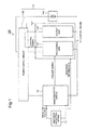
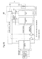
- FIG. 1 A schematic configuration diagram of a vibration detecting apparatus of an exemplary embodiment 1 is shown in Fig. 1 .
- the vibration detecting apparatus 100 of the present exemplary embodiment comprises, as primary constituent elements, a vibration detecting means 11, a semiconductor switch 12, a control means 13 and a power supply means 14.
- the semiconductor switch 12 and the control means 13 are connected with the power supply means 14.
- the vibration detecting means 11 is connected with the semiconductor switch 12.
- the semiconductor switch 12 is connected with the control means 13.
- the power supply means 14 is composed of a power supply 141 and a power supply circuit 142
- the control means 13 is composed of a processing unit 131 and an output unit 132 (transmission/reception unit).
- the vibration detecting means 11 is a vibration sensor, for example, which detects vibration of a structure, acquires vibration waveform data from the structure and then converts the data into a vibration voltage.
- the vibration voltage is transmitted to the semiconductor switch 12.
- the vibration sensor There is no particular restriction on the vibration sensor, and publicly known vibration sensors may be used. Specifically, an acceleration sensor, a velocity sensor, a displacement sensor and the like are mentioned, for example.
- the acceleration sensor is preferably a piezoelectric-type one with a built-in signal amplifier circuit.
- the vibration detecting means 11 (vibration sensor) is preferably one with high sensitivity and capability of detecting signals in a wide frequency band.
- a contact type vibration detecting means to be installed in a structure may be used, for example.
- the vibration detecting means 11 may be installed at an appropriate location in the structure in accordance with the use of the vibration detecting apparatus 100.
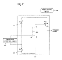
- FIG. 2 A structure of the semiconductor switch 12 in the present exemplary embodiment is shown in Fig. 2 .
- the semiconductor switch 12 is illustrated including a state of its connection with the vibration detecting means 11.
- the semiconductor switch 12 is a switch which comprises a voltage dividing means for generating a bias voltage inside, detects a voltage consisting of a vibration voltage outputted by the vibration detecting means 11 and of the bias voltage superposed onto the vibration voltage, and conducts current when the detected voltage is equal to or larger than a certain value.
- the semiconductor switch 12 converts the vibration voltage into a binary trigger signal according to the magnitude of the voltage value, and transmits the signal to the control means 13.
- voltage dividing resistors R1 and R2 are used as a voltage dividing means 121 in Fig.
- the present invention is not limited to that, and voltage dividing capacitors, converters or the like, for example, may also be used as the voltage dividing means 121.
- voltage dividing resistors are used as the voltage dividing means 121, there occurs power consumption but no voltage fluctuation.
- voltage dividing capacitors are used, power consumption is small but voltage fluctuation is easily generated. What kind of means is used as the voltage dividing means 121 may be determined according to the use of the vibration detecting apparatus.
- the semiconductor switch 12 is a switch comprising a semiconductor element, and the semiconductor switch 12 has a function to detect the above-described voltage and to conduct current when the voltage is equal to or larger than a certain value.
- the semiconductor element is, for example, a transistor, a field effect transistor (FET) or the like.
- FET field effect transistor
- the semiconductor switch is an FET, for example, the above-described voltage is detected as the gate voltage, and a drain current flows when the voltage is equal to or larger than a certain value.
- the semiconductor switch 12 comprises a channel FET (N-type channel MOSFET (Q1)) and a bipolar transistor (PNP transistor (Q2)).
- the above-described voltage dividing resistors includes a first and a second resistors (R1 and R2), and R1 and R2 each have a first and a second terminals.
- the vibration detecting means 11 also has a first and a second terminals. Then, the first terminal of R1 is electrically connected to the power supply means 14, the second terminal of R1 is electrically connected to the first terminal of R2 and to the second terminal of the vibration detecting means 11, and the second terminal of R2 is grounded.
- the first terminal of the vibration detecting means 11 is electrically connected to the gate of the channel FET, the source of the channel FET is grounded, the drain of the channel FET is electrically connected to the base of the bipolar transistor, the emitter of the bipolar transistor is electrically connected to the power supply means 14, and the collector of the bipolar transistor is electrically connected to the control means 13.
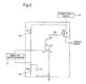
- one electrode of the vibration detecting means 11 is connected to an intermediate point between the voltage dividing resistors R1 and R2 of the semiconductor switch 12, and the other electrode is connected to the gate G of the N-type channel MOSFET (Q1).
- the drain D of the N-type channel MOSFET (Q1) is connected to the base B of the PNP transistor (Q2).
- the drain D of the N-type channel MOSFET (Q1) may be connected to the base B of the PNP transistor (Q2) via a limiting resistor R3, as shown in Fig. 3 .
- the emitter E of the PNP transistor (Q2) is connected to the power supply means 14, and the collector C is made an output port for a trigger signal.
- the vibration detecting means 11 when there is no vibration, the voltage difference between the two electrodes of the vibration detecting means 11 is zero, and accordingly, the potential at the intermediate point between the voltage dividing resistors R1 and R2 of the semiconductor switch 12 is the same as that at the gate G of the N-type channel MOSFET (Q1). Resistance values of the voltage dividing resistors R1 and R2 are set such that the potential at the intermediate point between R1 and R2 becomes slightly lower than the threshold voltage Vth of the N-type channel MOSFET (Q1). When there is no vibration, both of the N-type channel MOSFET (Q1) and the PNP transistor (Q2) are kept OFF. When there is a vibration, the vibration detecting means 11 generates a vibration voltage in accordance with the acceleration.
- the N-type channel MOSFET (Q1) becomes ON.
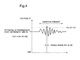
- Fig. 4 shown is a waveform of the gate voltage of the N-type channel MOSFET (Q1) for when the N-type channel MOSFET (Q1) changes its state as OFF ⁇ ON ⁇ OFF.
- the maximum amplitude of the vibration voltage is generally smaller than the threshold voltage Vth of the N-type channel MOSFET (Q1), the N-type channel MOSFET (Q1) can enter into the ON state in the present case, because the voltage between the gate G and the source S is biased in advance by the voltage dividing resistors R1 and R2 of the semiconductor switch 12.
- resistance values of the voltage dividing resistors R1 and R2 are preferably set to be equal to or larger than a few hundred kilo-ohms.
- a smoothing capacitor C1 may be disposed in order to prevent pulsating current due to fluctuation of the power supply voltage and false operation due to noise.
- the smoothing capacitor C1 (voltage dividing capacitor), which has a first and a second terminals, may be disposed with the first terminal being electrically connected to the first terminal of the second resistor R2, and with the second terminal being grounded.
- the control means 13 wakes up with the current conducted by the semiconductor switch 12 as a trigger signal.
- the control means 13 having waked up starts processing.
- the processing unit 131 of the control means 13 is a means for processing and detecting an output signal outputted from the vibration detecting means 11, which is a microcomputer or the like, for example.
- the processing unit 131 switches from a standby state being a power saving mode to a wake-up state.
- the processing unit 131 transmits a control signal to the power supply circuit 142.
- the power supply circuit 142 supplies power to the output unit 132.
- the vibration voltage is transmitted to the processing unit 131 as vibration information.
- the processing unit 131 for example, filtering with a frequency based on a sampling frequency and subsequent computational processing into a digital signal are performed on the vibration information, and the resultant signal is transmitted to the output unit 132.
- the output unit 132 of the control means 13 sends the digital signal after modulating it into a signal waveform able to be sent.
- the output unit 132 may comprise an antenna, and the output signal may be sent in the form of a radio signal.
- Analysis of the vibration information may be performed by the processing unit 131 or the output unit 132, or by another analysis means to which the vibration information is sent from the output unit 132.
- the processing unit 131 switches again to the standby state being a power saving mode and prepares for the next vibration.
- the embodiment has been shown to be the one in which the vibration voltage is transmitted to the processing unit 131 as vibration information and is processed there, but the present invention is not limited to that, and the trigger signal itself may be used as vibration information, for example.
- the vibration detecting apparatus of the present exemplary embodiment 1 can detect a weak signal, while being power saving, because a bias voltage is superposed onto the vibration voltage by the voltage dividing means. Further, the vibration detecting apparatus can perform start-up of the apparatus and collection of vibration information (data) by the use of only one vibration detecting means.
- FIG. 5 A structure of a semiconductor switch 12A in a modified example of the present exemplary embodiment 1 is shown in Fig. 5 .
- the semiconductor switch 12A is illustrated including a state of its connection with the vibration detecting means 11.
- the semiconductor switch 12A comprises a channel FET (P-type channel MOSFET (Q3)) and a bipolar transistor (NPN transistor (Q4)).
- Voltage dividing resistors include a first and a second resistors (R4 and R5), and R4 and R5 each have a first and a second terminals.
- the vibration detecting means 11 also has a first and a second terminals.
- the first terminal of R4 is electrically connected to the power supply means 14, the second terminal of R4 is electrically connected to the first terminal of R5 and to the first terminal of the vibration detecting means 11, and the second terminal of R5 is grounded.
- the second terminal of the vibration detecting means 11 is electrically connected to the gate of the channel FET, the drain of the channel FET is electrically connected to the power supply means 14, the source of the channel FET is electrically connected to the base of the bipolar transistor, the emitter of the bipolar transistor is electrically connected to the control means 13, and the collector of the bipolar transistor is electrically connected to the power supply means 14.
- one electrode of the vibration detecting means 11 is connected to an intermediate point between the voltage dividing resistors R4 and R5 of the semiconductor switch 12A, and the other electrode is connected to the gate G of the P-type channel MOSFET (Q3).
- the source S of the P-type channel MOSFET (Q3) is connected to the base B of the NPN transistor (Q4) via a limiting resistor R6.
- the collector C of the NPN transistor (Q4) is connected to the power supply means 14, and the emitter E is made an output port for a trigger signal.
- the vibration detecting means 11 when there is no vibration, the voltage difference between the two electrodes of the vibration detecting means 11 is zero, and accordingly, the potential at the intermediate point between the voltage dividing resistors R4 and R5 of the semiconductor switch 12A is the same as that at the gate G of the P-type channel MOSFET (Q3). Resistance values of the voltage dividing resistors R4 and R5 are set such that the potential at the intermediate point between R4 and R5 becomes slightly lower than the threshold voltage Vth of the P-type channel MOSFET (Q3). When there is no vibration, both of the P-type channel MOSFET (Q3) and the NPN transistor (Q4) are kept OFF. When there is a vibration, the vibration detecting means 11 generates a vibration voltage in accordance with the acceleration.
- the P-type channel MOSFET (Q3) When the voltage between the gate G and the source S of the P-type channel MOSFET (Q3) exceeds the specific threshold voltage Vth, the P-type channel MOSFET (Q3) becomes ON.
- Fig. 6 shown is a waveform of the gate voltage of the P-type channel MOSFET (Q3) for when the P-type channel MOSFET (Q3) changes its state as OFF ⁇ ON ⁇ OFF.
- the maximum amplitude of the vibration voltage is generally smaller than the threshold voltage Vth of the P-type channel MOSFET (Q3), the P-type channel MOSFET (Q3) can enter into the ON state in the present case, because the voltage between the gate G and the source S is biased in advance by the voltage dividing resistors R4 and R5 of the semiconductor switch 12A.
- resistance values of the voltage dividing resistors R4 and R5 are preferably set to be equal to or larger than a few hundred kilo-ohms.
- the NPN transistor (Q4) is an optional constituent member, it is preferably included because, if it is included, a signal amplified by the NPN transistor (Q4) can be outputted even when a voltage change at the gate G of the P-type channel MOSFET (Q3) is small, that is, even when the vibration detecting means 11 has a characteristic of outputting only a weak signal.
- a smoothing capacitor C2 may be disposed in order to prevent pulsating current due to fluctuation of the power supply voltage and false operation due to noise.
- the smoothing capacitor C2 (voltage dividing capacitor), which has a first and a second terminals, may be disposed with the first terminal being electrically connected to the power supply unit 14, and with the second terminal being electrically connected to the second terminal of the first resistor R4.
- the semiconductor switch 12A comprises the smoothing capacitor C2 in Fig. 5
- the present invention is not limited to that, and the semiconductor switch 12A does not necessarily need to comprise the smoothing capacitor C2.
- voltage dividing capacitors may be used in place of the voltage dividing resistors R4 and R5, for the purpose of dividing the supply voltage.
- a semiconductor switch comprises a voltage doubling circuit. Except for that point, a vibration detecting apparatus and a vibration detection method of the present exemplary embodiment are the same as those of the exemplary embodiment 1.
- a structure of a semiconductor switch 22 in the present exemplary embodiment is shown in Fig. 7 .
- the semiconductor switch 22 is the same as the semiconductor switch 12 in Fig. 3 , except that a half-wave voltage doubler rectifying circuit (voltage doubling circuit) 25 composed of capacitors C3 and C4 and of diodes D1 and D2 is added between the vibration detecting means 11 and the N-type channel MOSFET (Q1).
- a half-wave voltage doubler rectifying circuit (voltage doubling circuit) 25 composed of capacitors C3 and C4 and of diodes D1 and D2 is added between the vibration detecting means 11 and the N-type channel MOSFET (Q1).
- FIG. 8 A structure of a semiconductor switch 22A in a modified example of the present exemplary embodiment 2 is shown in Fig. 8 .
- the semiconductor switch 22A is the same as the semiconductor switch 12A in Fig. 5 , except that a half-wave voltage doubler rectifying circuit (voltage doubling circuit) 25A composed of capacitors C5 and C6 and of diodes D3 and D4 is added between the vibration detecting means 11 and the P-type channel MOSFET (Q3).
- a trigger signal can be transmitted from the semiconductor switch 22A even when the vibration voltage is further small.
- a trigger signal can be transmitted from the semiconductor switch even when the vibration voltage is further small, because the semiconductor switch comprises the voltage doubling circuit and can accordingly double the vibration voltage by the use of the voltage doubling circuit.
- a vibration detecting apparatus further comprises a voltage amplification means. Except for that point, the vibration detecting apparatus and a vibration detection method of the present exemplary embodiment are the same as those of the exemplary embodiment 1.
- FIG. 9 A schematic configuration diagram of the vibration detecting apparatus of the exemplary embodiment 3 is shown in Fig. 9 .
- the vibration detecting apparatus 300 of the present exemplary embodiment is the same as the vibration detecting apparatus 100 in Fig. 1 , except that the semiconductor switch 12 and a voltage amplification means 36 are connected to the vibration detecting means 11 and to the control means 13 via signal lines.
- the processing unit 131 switches from a standby state being a power saving mode to a wake-up state.
- the processing unit 131 transmits a control signal to the power supply circuit 142.
- the power supply circuit 142 supplies power to the voltage amplification means 36 and the output unit 132.
- a vibration voltage is transmitted to the voltage amplification means 36.
- the vibration voltage is amplified by the voltage amplification means 36 and then transmitted to the processing unit 131 as vibration information. In this way, the vibration voltage can be made to be analyzable level of vibration information by means of the voltage amplification means 36.
- the vibration detecting apparatus of the present exemplary embodiment 3 can obtain vibration information of analyzable level even when the vibration voltage is further small, because it further comprises the voltage amplification means.
- a piezoelectric sensor may be used as the vibration detecting means 11.
- the piezoelectric sensor is made of a piezoelectric ceramic. Because the piezoelectric sensor itself works also as a power generation source, an external power supply becomes unnecessary, and further power saving is accordingly achieved. Further, because using the piezoelectric sensor as the vibration detecting means makes it possible to fabricate the vibration detecting means into a relatively simple structure with an unrestricted shape, the vibration detecting apparatus can be reduced in size.
- a semiconductor-type sensor may be used as the vibration detecting means 11.
- acceleration can be measured even when the acceleration does not change in a manner like that of alternating current, because a voltage proportional to the magnitude of the acceleration is outputted as a result of a change in capacitance in the silicon chip.
- a vibration detecting apparatus further comprises a charge-voltage conversion means (charge amplifier). Except for that point, the vibration detecting apparatus and a vibration detection method of the present exemplary embodiment are the same as those of the exemplary embodiment 3.
- FIG. 10 A schematic configuration diagram of the vibration detecting apparatus of the exemplary embodiment 4 is shown in Fig. 10 .
- the vibration detecting apparatus 400 of the present exemplary embodiment is the same as the vibration detecting apparatus 300 in Fig. 9 , except that a charge amplifier 47 is disposed between the vibration detecting means 11 and the voltage amplification means 36.
- a trigger signal is transmitted from the semiconductor switch 12 to the control means 13
- the processing unit 131 switches from a standby state being a power saving mode to a wake-up state.
- the processing unit 131 transmits a control signal to the power supply circuit 142.
- the power supply circuit 142 supplies power to the charge amplifier 47, the voltage amplification means 36 and the output unit 132.
- a vibration voltage is transmitted to the voltage amplification means 36 via the charge amplifier 47.
- the vibration detecting apparatus of the present exemplary embodiment 4 it is possible to prevent change of the vibration voltage due to change in capacitance between the vibration detecting means and the voltage amplification means, and accordingly to perform vibration detection more precisely, because the charge amplifier is further comprised.
- the vibration detecting apparatuses and the vibration detection methods of the present invention can be applied to, for example, a water-leakage detecting apparatus and a water-leakage detecting method.
- an installation location for the vibration detecting means of the vibration detecting apparatus may be, for example, a water pipe such as an intake pipe, a conducting pipe, a supplying pipe and a feeding pipe, a manhole, a hydrant, a shutoff valve or the like.
- a water pipe such as an intake pipe, a conducting pipe, a supplying pipe and a feeding pipe, a manhole, a hydrant, a shutoff valve or the like.
- a bias voltage generated by the voltage dividing means is superposed onto the vibration voltage, the voltage produced by the superposition is then detected, and a trigger signal is transmitted if the detected voltage is equal to or larger than a certain value. Then, the control means wakes up by the trigger signal.
- the control means having waked up starts performing a control process.
- the control process mentioned are analyses of the vibration waveform for identifying the abnormality in the conducting pipe, notification of the water leakage by an alarm and the like, for example.
- voltage dividing resistors may be preferably used as the voltage dividing means in the semiconductor switch. Voltage dividing resistors may be preferably used because they have characteristics of small voltage fluctuation and small voltage change due to temperature change.
- the vibration detecting apparatuses and the vibration detecting methods of the present invention can be applied to a water-leakage detecting apparatus and a water-leakage detecting method.
- the vibration detecting apparatuses and the vibration detecting methods of the present invention can be applied to an intrusion detecting apparatus and an intrusion detecting method.
- an installation location for the vibration detecting apparatus may be, for example, a window frame, glass, a door, a floor surface, the ground surface or the like.
- Vibration caused by abnormal vibration or abnormal sound due to an intrusion action is detected by the vibration detecting means, and then the control means wakes up similarly to in the exemplary embodiment 5.
- the control means having waked up starts performing a control process.
- the control process mentioned are analyses of the vibration waveform for identifying the intrusion action, operation of a surveillance camera, activation of a security buzzer and the like, for example.
- the vibration detecting apparatuses and the vibration detecting methods of the present invention can be applied to an intrusion detecting apparatus and an intrusion detecting method.
- the vibration detecting apparatuses and the vibration detecting methods of the present invention can be applied to an abnormality detecting apparatus and an abnormality detecting method used in, for example, product inspection at a time of factory shipment.
- an installation location for the vibration detecting means of the vibration detecting apparatus may be, for example, on a conveyance means for conveying the products, such as a conveyer belt, or the like.
- a conveyance means for conveying the products such as a conveyer belt, or the like.
- Vibration caused by the abnormal vibration or abnormal sound is detected by the vibration detecting means, and then the control means wakes up similarly to in the exemplary embodiment 5.
- the control means having waked up starts performing a control process.
- the control process mentioned are analyses of the vibration waveform for identifying the abnormality of the product, notification of the abnormality of the product by an alarm, and the like, for example.
- the vibration detecting apparatuses and the vibration detecting methods of the present invention can be applied to an abnormality detecting apparatus and an abnormality detecting method such as described above.
- the vibration detecting apparatuses and the vibration detecting methods of the present invention can be applied to a deterioration detecting apparatus and a deterioration detecting method used for, for example, a device such as a motor.
- an installation location for the vibration detecting means of the vibration detecting apparatus may be, for example, on the housing of a motor or the like, on a stand with a motor or the like installed thereon, and the like.
- the control means wakes up similarly to in the exemplary embodiment 5.
- the control means having waked up starts performing a control process.
- the control process mentioned are analyses of the vibration waveform for identifying the deterioration of the device, notification of deterioration of a structure by an alarm, and the like, for example.
- the vibration detecting apparatuses and the vibration detecting methods of the present invention can be applied to a deterioration detecting apparatus and a deterioration detecting method used for a device.
- the vibration detecting apparatuses and the vibration detecting methods of the present invention can be applied to, for example, a security-related use such as intrusion detection, detection of water leakage or of destruction of a water pipe in a water pipeline system of a social infrastructure business, detection of deterioration of a structure such as a building or a house, detection of petroleum leakage or of destruction of a pipeline in a petroleum pipeline system, detection of gas leakage or of destruction of a pipeline in a gas pipeline system, detection of abnormality of general devices such as a motor, inspection at a time of product shipment, and the like, and thus, they can be applied unlimitedly to a wide variety of uses.
- a security-related use such as intrusion detection, detection of water leakage or of destruction of a water pipe in a water pipeline system of a social infrastructure business, detection of deterioration of a structure such as a building or a house, detection of petroleum leakage or of destruction of a pipeline in a petroleum pipeline system, detection of gas leakage or of destruction of a
Landscapes
- Physics & Mathematics (AREA)
- General Physics & Mathematics (AREA)
- Measurement Of Mechanical Vibrations Or Ultrasonic Waves (AREA)
Applications Claiming Priority (2)
| Application Number | Priority Date | Filing Date | Title |
|---|---|---|---|
| JP2012137339 | 2012-06-18 | ||
| PCT/JP2012/082039 WO2013190727A1 (ja) | 2012-06-18 | 2012-12-11 | 振動検出装置および振動検出方法 |
Publications (2)
| Publication Number | Publication Date |
|---|---|
| EP2863191A1 true EP2863191A1 (de) | 2015-04-22 |
| EP2863191A4 EP2863191A4 (de) | 2015-10-28 |
Family
ID=49768344
Family Applications (1)
| Application Number | Title | Priority Date | Filing Date |
|---|---|---|---|
| EP12879337.9A Withdrawn EP2863191A4 (de) | 2012-06-18 | 2012-12-11 | Vibrationserkennungsvorrichtung und vibrationserkennungsverfahren |
Country Status (4)
| Country | Link |
|---|---|
| US (1) | US9664554B2 (de) |
| EP (1) | EP2863191A4 (de) |
| JP (1) | JPWO2013190727A1 (de) |
| WO (1) | WO2013190727A1 (de) |
Families Citing this family (6)
| Publication number | Priority date | Publication date | Assignee | Title |
|---|---|---|---|---|
| JP6410148B2 (ja) * | 2014-02-25 | 2018-10-24 | パナソニックIpマネジメント株式会社 | 衝撃記憶装置 |
| JP6293537B2 (ja) * | 2014-03-19 | 2018-03-14 | 株式会社東芝 | 検査システム、及び異常検出方法 |
| US9940521B2 (en) * | 2015-02-27 | 2018-04-10 | Sony Corporation | Visibility enhancement devices, systems, and methods |
| CN106154347A (zh) * | 2015-04-27 | 2016-11-23 | 鸿富锦精密工业(武汉)有限公司 | 距离检测系统、振动提示电路及振动提示方法 |
| JP7313252B2 (ja) * | 2019-10-08 | 2023-07-24 | 東京エレクトロン株式会社 | リーク測定システム、半導体製造システム及びリーク測定方法 |
| CA3191864A1 (en) * | 2020-08-21 | 2022-02-24 | Agc Glass Europe | Glazing with a reusable vibration sensor |
Family Cites Families (15)
| Publication number | Priority date | Publication date | Assignee | Title |
|---|---|---|---|---|
| CH643078A5 (de) | 1978-11-30 | 1984-05-15 | Cerberus Ag | Verfahren und anordnung zur einbruchmeldung. |
| JPS59148598A (ja) * | 1983-02-09 | 1984-08-25 | Matsushita Electric Ind Co Ltd | ステツピングモ−タ駆動回路 |
| US5621627A (en) * | 1995-04-14 | 1997-04-15 | Ac International Inc. | A.C. to A.C. power converter for the adaptive correction of waveform abnormalities |
| US5510944A (en) * | 1995-05-05 | 1996-04-23 | U.S. Philips Corporation | Power supply over-voltage protection |
| US6801247B1 (en) * | 1996-12-12 | 2004-10-05 | Nikon Corporation | Vibration reduction device and vibration detecting device and micro signal processing device for use in vibration reduction device |
| JP3911854B2 (ja) * | 1998-06-25 | 2007-05-09 | 松下電器産業株式会社 | 振動検出装置 |
| JP2002346474A (ja) * | 2001-05-23 | 2002-12-03 | Sanyo Electric Co Ltd | 体感振動式告知装置 |
| JP2003346107A (ja) | 2002-05-27 | 2003-12-05 | Totoku Electric Co Ltd | 無線式物品管理タグおよび物品管理システム |
| JP2006126095A (ja) | 2004-10-29 | 2006-05-18 | Nec San-Ei Instruments Ltd | センサの異状検出装置及びセンサの異状検出方法並びに加速度測定装置と加速度測定方法 |
| JP2006349409A (ja) * | 2005-06-14 | 2006-12-28 | Denso Corp | 静電駆動・容量検出型のジャイロセンサのセンサ回路 |
| US7430914B2 (en) * | 2005-09-16 | 2008-10-07 | Mitsui Babcock (Us) Llc | Vibration analyzing device |
| US7377171B2 (en) | 2006-08-15 | 2008-05-27 | General Electric Company | Feedback circuit for radiation resistant transducer |
| JP2008186336A (ja) | 2007-01-31 | 2008-08-14 | Yaskawa Electric Corp | センサ装置 |
| JP2009273201A (ja) | 2008-05-01 | 2009-11-19 | Hyper Drive Corp | 電場応答性高分子を用いた発電装置 |
| JP2011221002A (ja) * | 2010-03-25 | 2011-11-04 | Sanyo Electric Co Ltd | 振動検出装置、空気圧検出端末および加速度検出システム |
-
2012
- 2012-12-11 EP EP12879337.9A patent/EP2863191A4/de not_active Withdrawn
- 2012-12-11 WO PCT/JP2012/082039 patent/WO2013190727A1/ja not_active Ceased
- 2012-12-11 US US14/408,574 patent/US9664554B2/en active Active
- 2012-12-11 JP JP2014521195A patent/JPWO2013190727A1/ja active Pending
Also Published As
| Publication number | Publication date |
|---|---|
| US9664554B2 (en) | 2017-05-30 |
| JPWO2013190727A1 (ja) | 2016-02-08 |
| EP2863191A4 (de) | 2015-10-28 |
| US20150160071A1 (en) | 2015-06-11 |
| WO2013190727A1 (ja) | 2013-12-27 |
Similar Documents
| Publication | Publication Date | Title |
|---|---|---|
| US9664554B2 (en) | Vibration detecting apparatus and vibration detecting method | |
| US11029196B2 (en) | Vibration sensor for fluid leak detection | |
| US20160093187A1 (en) | Sound and Temperature Sensors for Environmental Anomaly Detection | |
| CN105785936B (zh) | 无线工业过程监控器 | |
| US6310555B1 (en) | Water leak detector | |
| US20130154660A1 (en) | System and method for ground fault detection and fault type evaluation | |
| US20080238662A1 (en) | System, method, and kit for remotely monitoring an individual with a sensor-integrated picture frame | |
| KR20170047270A (ko) | 포털 보안 검출 기구 | |
| MY198437A (en) | Foreign Object Detection In A Wireless Power Transfer System | |
| WO2017035928A1 (zh) | 智能报警系统及方法 | |
| US20170268954A1 (en) | Pipeline Wireless Sensor Network | |
| EP1343016A3 (de) | Erkennungseinrichtung von Verdrahtungsfehlern für Klimaanlage | |
| US20190064092A1 (en) | Liquid detection device and liquid detection system | |
| EP4245992A3 (de) | Zustandsüberwachungsvorrichtung, zustandsüberwachungssystem und zustandsüberwachungsverfahren | |
| KR20170127923A (ko) | IoT 기반 가스 누출 원격 모니터링 시스템 | |
| JPH1114663A (ja) | 物理量センサ | |
| CN109163838A (zh) | 基于压力传感器的紧固件监测装置 | |
| WO2014024559A1 (ja) | 振動検出装置 | |
| US8548765B2 (en) | Dynamically self-adjusting sensor | |
| KR20190054376A (ko) | 자가 점검 기능이 내장된 무선수신장치 | |
| TW200632340A (en) | Method for non-contact testing of fixed and inaccessible connections without using a sensor plate | |
| US20160034010A1 (en) | Electronic device having a programmed electrical characteristic | |
| CN218885869U (zh) | 气体探测模组及气体传感器的控制电路 | |
| US20250290955A1 (en) | Electrostatic charge variation based power failure detection | |
| CN211877113U (zh) | 一种基于工业互联网的数据监控系统 |
Legal Events
| Date | Code | Title | Description |
|---|---|---|---|
| PUAI | Public reference made under article 153(3) epc to a published international application that has entered the european phase |
Free format text: ORIGINAL CODE: 0009012 |
|
| 17P | Request for examination filed |
Effective date: 20141218 |
|
| AK | Designated contracting states |
Kind code of ref document: A1 Designated state(s): AL AT BE BG CH CY CZ DE DK EE ES FI FR GB GR HR HU IE IS IT LI LT LU LV MC MK MT NL NO PL PT RO RS SE SI SK SM TR |
|
| AX | Request for extension of the european patent |
Extension state: BA ME |
|
| RIN1 | Information on inventor provided before grant (corrected) |
Inventor name: YOSHINARI, TETSUYA Inventor name: SHINODA, SHIGEKI Inventor name: ABE, KATSUMI Inventor name: KADOSAWA, HIDEKI Inventor name: SASAKI, YASUHIRO |
|
| DAX | Request for extension of the european patent (deleted) | ||
| RA4 | Supplementary search report drawn up and despatched (corrected) |
Effective date: 20150928 |
|
| RIC1 | Information provided on ipc code assigned before grant |
Ipc: G08B 13/16 20060101ALI20150922BHEP Ipc: G01H 11/08 20060101AFI20150922BHEP |
|
| GRAP | Despatch of communication of intention to grant a patent |
Free format text: ORIGINAL CODE: EPIDOSNIGR1 |
|
| INTG | Intention to grant announced |
Effective date: 20181026 |
|
| STAA | Information on the status of an ep patent application or granted ep patent |
Free format text: STATUS: THE APPLICATION IS DEEMED TO BE WITHDRAWN |
|
| 18D | Application deemed to be withdrawn |
Effective date: 20190306 |