EP2863652A1 - Dispositif d'auto-adaptation d'interface audio - Google Patents
Dispositif d'auto-adaptation d'interface audio Download PDFInfo
- Publication number
- EP2863652A1 EP2863652A1 EP20130804848 EP13804848A EP2863652A1 EP 2863652 A1 EP2863652 A1 EP 2863652A1 EP 20130804848 EP20130804848 EP 20130804848 EP 13804848 A EP13804848 A EP 13804848A EP 2863652 A1 EP2863652 A1 EP 2863652A1
- Authority
- EP
- European Patent Office
- Prior art keywords
- pin
- resistor
- conductive component
- switching module
- audio interface
- Prior art date
- Legal status (The legal status is an assumption and is not a legal conclusion. Google has not performed a legal analysis and makes no representation as to the accuracy of the status listed.)
- Granted
Links
Images


Classifications
-
- H—ELECTRICITY
- H04—ELECTRIC COMMUNICATION TECHNIQUE
- H04R—LOUDSPEAKERS, MICROPHONES, GRAMOPHONE PICK-UPS OR LIKE ACOUSTIC ELECTROMECHANICAL TRANSDUCERS; ELECTRIC HEARING AIDS; PUBLIC ADDRESS SYSTEMS
- H04R3/00—Circuits for transducers
-
- H—ELECTRICITY
- H04—ELECTRIC COMMUNICATION TECHNIQUE
- H04R—LOUDSPEAKERS, MICROPHONES, GRAMOPHONE PICK-UPS OR LIKE ACOUSTIC ELECTROMECHANICAL TRANSDUCERS; ELECTRIC HEARING AIDS; PUBLIC ADDRESS SYSTEMS
- H04R5/00—Stereophonic arrangements
- H04R5/04—Circuit arrangements, e.g. for selective connection of amplifier inputs/outputs to loudspeakers, for loudspeaker detection, or for adaptation of settings to personal preferences or hearing impairments
-
- H—ELECTRICITY
- H04—ELECTRIC COMMUNICATION TECHNIQUE
- H04R—LOUDSPEAKERS, MICROPHONES, GRAMOPHONE PICK-UPS OR LIKE ACOUSTIC ELECTROMECHANICAL TRANSDUCERS; ELECTRIC HEARING AIDS; PUBLIC ADDRESS SYSTEMS
- H04R2201/00—Details of transducers, loudspeakers or microphones covered by H04R1/00 but not provided for in any of its subgroups
- H04R2201/10—Details of earpieces, attachments therefor, earphones or monophonic headphones covered by H04R1/10 but not provided for in any of its subgroups
- H04R2201/107—Monophonic and stereophonic headphones with microphone for two-way hands free communication
-
- H—ELECTRICITY
- H04—ELECTRIC COMMUNICATION TECHNIQUE
- H04R—LOUDSPEAKERS, MICROPHONES, GRAMOPHONE PICK-UPS OR LIKE ACOUSTIC ELECTROMECHANICAL TRANSDUCERS; ELECTRIC HEARING AIDS; PUBLIC ADDRESS SYSTEMS
- H04R2420/00—Details of connection covered by H04R, not provided for in its groups
- H04R2420/05—Detection of connection of loudspeakers or headphones to amplifiers
Definitions
- the present disclosure relates to an electronic technique field, and more particularly relates to an audio interface self-adaption device.
- An audio interface (such as a headphone jack) of a conventional audio signal sending device (such as a mobile communication terminal) or an audio interface of a conventional audio interface receiving device (such as a headphone) is generally a four-section interface, where a pin 1 and a pin 2 are audio pins, namely a left-channel pin and a right-channel pin.
- a pin 3 and a pin 4 have different functions in different audio interfaces, however, there are two types of audio interfaces.
- the pin 3 is a microphone pin (MIC pin) and the pin 4 is a ground pin (GND pin).
- the pin 3 is a GND pin
- the pin 4 is a MIC pin.
- an audio interface of an audio signal sending device such as a mobile communication terminal
- an audio interface of an audio signal receiving device such as a earphone or a headphone
- the audio signal sending device and the audio signal receiving device can neither communicate with each other via the MIC pin of the audio interface, nor transmit audio signals between each other normally using the audio pins (a left-channel pin and a right channel-pin) of the audio interface.
- an audio interface self-adaption device that can adapt to audio signal send devices (such as mobile communication terminals) having different audio interfaces is required.
- the technical problem the present disclosure seeks to solve is to overcome at least one disadvantages in the related art, and to provide an audio interface self-adaption device that can adapt to audio signal send devices having different audio interfaces.
- an audio interface self-adaption device comprises an audio interface comprising a pin 1, a pin 2, a pin 3, and a pin 4; one of the pin 3 and the pin 4 is a microphone pin of the audio interface, and the other one of the pin 3 and the pin 4 is a ground pin of the audio interface.
- the device further comprises a first level comparison module, a second level comparison module, a PNP triode Tc, a power output terminal VBAT, a switching module, a resistor R2a, and a resistor R2b, where:
- the device further comprises a first unidirectional conductive component, a second unidirectional conductive component, and a resistor R4; the audio pin is connected to the pin 3 via the first unidirectional conductive component, and the audio pin is connected to the pin 4 via the second unidirectional conductive component; a conducting direction of the first unidirectional conductive component is from the audio pin to the pin 3, and a conducting direction of the second unidirectional conductive component is from the audio pin to the pin 4; and the pin 3 and the pin 4 of the audio interface are connected via the resistor R4.
- the audio pin comprises the pin 1 and the pin 2 of the audio interface; the pin 1 is connected to the first unidirectional conductive component via a first signal processing module, the first unidirectional conductive component is connected to the pin 3, and the pin 1 is connected to the pin 4 via the first signal processing module and the second unidirectional conductive component; and the pin 2 is connected to the first unidirectional conductive component via a second signal processing module, the first unidirectional conductive component is connected to the pin 3, and the pin 2 is connected to the pin 4 via the second signal processing module and the second unidirectional conductive component.
- the first unidirectional conductive component comprises one selected from a group consisting of: a diode, a triode, and a MOS; and the second unidirectional conductive component comprises one selected from a group consisting of: a diode, a triode, and a MOS.
- the first signal processing module comprises at least one selected from a group consisting of: a resistor, a microphone, a transformer, a resistor, and a comparator connected in parallel, and a resistor and an operational amplifier connected in parallel; and the second signal processing module comprises at least one selected from a group consisting of: a resistor, a microphone, a transformer, a resistor and a comparator connected in parallel, and a resistor and an operational amplifier connected in parallel.
- the audio interface is a headphone plug or a headphone jack.
- Embodiments of the present disclosure provide an audio interface self-adaption device.
- the device comprises an audio interface; the audio interface comprises a pin 1, a pin 2, a pin 3, and a pin 4; one of the pin 3 and the pin 4 is a microphone pin of the audio interface, and the other one of the pin 3 and the pin 4 is a ground pin of the audio interface.
- the device further comprises a first level comparison module, a second level comparison module, a PNP triode Tc, a power output terminal VBAT, a switching module, a resistor R2a, and a resistor R2b; where:
- the device further comprises a first unidirectional conductive component, a second unidirectional conductive component, and a resistor R4; the audio pin is connected to the pin 3 via the first unidirectional conductive component, and the audio pin is connected to the pin 4 via the second unidirectional conductive component; a conducting direction of the first unidirectional conductive component is from the audio pin to the pin 3, and a conducting direction of the second unidirectional conductive component is from the audio pin to the pin 4; and the pin 3 and the pin 4 of the audio interface are connected via the resistor R4.
- the audio pin is the pin 1 and the pin 2 of the audio interface; the pin 1 is connected to the first unidirectional conductive component via a first signal processing module, the first unidirectional conductive component is connected to the pin 3, and the pin 1 is connected to the pin 4 via the first signal processing module and the second unidirectional conductive component; and the pin 2 is connected to the first unidirectional conductive component via a second signal processing module, the first unidirectional conductive component is connected to the pin 3, and the pin 2 is connected to the pin 4 via the second signal processing module and the second unidirectional conductive component.
- the first unidirectional conductive component comprises one selected from a group consisting of: a diode, a triode, and a MOS; and the second unidirectional conductive component comprises one selected from a group consisting of: a diode, a triode, and a MOS.
- the first signal processing module comprises at least one selected from a group consisting of: a resistor, a microphone, a transformer, a resistor and a comparator connected in parallel, and a resistor and an operational amplifier connected in parallel; and the second signal processing module comprises at least one selected from a group consisting of: a resistor, a microphone, a transformer, a resistor and a comparator connected in parallel, and a resistor and an operational amplifier connected in parallel.
- the audio interface is a headphone plug or a headphone jack.
- Embodiments of the present disclosure provide an audio interface self-adaption device.
- the device comprises an audio interface; the audio interface comprises a pin 1, a pin 2, a pin 3, and a pin 4; one of the pin 3 and the pin 4 is a microphone pin of the audio interface, and the other one of the pin 3 and the pin 4 is a ground pin of the audio interface.
- the device further comprises a first level comparison module, a second level comparison module, a PNP triode Tc, a power output terminal VBAT, a switching module, a resistor R2a, and a resistor R2b, where:
- the device further comprises a first unidirectional conductive component, a second unidirectional conductive component, and a resistor R4; the audio pin is connected to the pin 3 via the first unidirectional conductive component, and the audio pin is connected to the pin 4 via the second unidirectional conductive component; a conducting direction of the first unidirectional conductive component is from the audio pin to the pin 3, and a conducting direction of the second unidirectional conductive component is from the audio pin to the pin 4; and the pin 3 and the pin 4 of the audio interface are connected via the resistor R4.
- the audio pin is the pin 1 and the pin 2 of the audio interface; the pin 1 is connected to the first unidirectional conductive component via a first signal processing module, the first unidirectional conductive component is connected to the pin 3, and the pin 1 is connected to the pin 4 via the first signal processing module and the second unidirectional conductive component; and the pin 2 is connected to the first unidirectional conductive component via a second signal processing module, the first unidirectional conductive component is connected to the pin 3, and the pin 2 is connected to the pin 4 via the second signal processing module and the second unidirectional conductive component.
- the first unidirectional conductive component comprises one selected from a group consisting of: a diode, a triode, and a MOS; and the second unidirectional conductive component comprises one selected from a group consisting of: a diode, a triode, and a MOS.
- the first signal processing module comprises at least one selected from a group consisting of: a resistor, a microphone, a transformer, a resistor and a comparator connected in parallel, and a resistor and an operational amplifier connected in parallel; and the second signal processing module comprises at least one selected from a group consisting of: a resistor, a microphone, a transformer, a resistor and a comparator connected in parallel, and a resistor and an operational amplifier connected in parallel.
- the audio interface is a headphone plug or a headphone jack.
- Embodiments of the present disclosure provide an audio interface self-adaption device.
- the device comprises an audio interface; the audio interface comprises a pin 1, a pin 2, a pin 3 and a pin 4; one of the pin 3 and the pin 4 is a microphone pin of the audio interface, and the other one of the pin 3 and the pin 4 is a ground pin of the audio interface.
- the device further comprises a first level comparison module, a second level comparison module, a power output terminal VBAT, a first switching module, a second switching module, and a resistor R2a, a resistor R2b, a resistor R3a, and a resistor R3b; where:
- the device further comprises a first unidirectional conductive component, a second unidirectional conductive component, and a resistor R4; the audio pin is connected to the pin 3 via the first unidirectional conductive component, and the audio pin is connected to the pin 4 via the second unidirectional conductive component; a conducting direction of the first unidirectional conductive component is from the audio pin to the pin 3, and a conducting direction of the second unidirectional conductive component is from the audio pin to the pin 4; and the pin 3 and the pin 4 of the audio interface are connected via the resistor R4.
- the audio pin is the pin 1 and the pin 2 of the audio interface; the pin 1 is connected to the first unidirectional conductive component via a first signal processing module, the first unidirectional conductive component is connected to the pin 3, and the pin 1 is connected to the pin 4 via the first signal processing module and the second unidirectional conductive component; and the pin 2 is connected to the first unidirectional conductive component via a second signal processing module, the first unidirectional conductive component is connected to the pin 3, and the pin 2 is connected to the pin 4 via the second signal processing module and the second unidirectional conductive component.
- the first unidirectional conductive component comprises one selected from a group consisting of: a diode, a triode, and a MOS; and the second unidirectional conductive component comprises one selected from a group consisting of: a diode, a triode, and a MOS.
- the first signal processing module comprises at least one selected from a group consisting of: a resistor, a microphone, a transformer, a resistor and a comparator connected in parallel, and a resistor and an operational amplifier connected in parallel; and the second signal processing module comprises at least one selected from a group consisting of: a resistor, a microphone, a transformer, a resistor and a comparator connected in parallel, and a resistor and an operational amplifier connected in parallel.
- the audio interface is a headphone plug or a headphone jack.
- Embodiments of the present disclosure provide an audio interface self-adaption device.
- the device comprises an audio interface; the audio interface comprises a pin 1, a pin 2, a pin 3, and a pin 4; one of the pin 3 and the pin 4 is a microphone pin of the audio interface, and the other one of the pin 3 and the pin 4 is a ground pin.
- the device further comprises a first level comparison module, a second level comparison module, a power output terminal VBAT, a first switching module, and a second switching module; where:
- the device further comprises a first unidirectional conductive component, a second unidirectional conductive component, and a resistor R4; the audio pin is connected to the pin 3 via the first unidirectional conductive component, and the audio pin is connected to the pin 4 via the second unidirectional conductive component; a conducting direction of the first unidirectional conductive component is from the audio pin to the pin 3, and a conducting direction of the second unidirectional conductive component is from the audio pin to the pin 4; and the pin 3 and the pin 4 of the audio interface are connected via the resistor R4.
- the audio pin comprises the pin 1 and the pin 2 of the audio interface; the pin 1 is connected to the first unidirectional conductive component via a first signal processing module, the first unidirectional conductive component is connected to the pin 3, and the pin 1 is connected to the pin 4 via the first signal processing module and the second unidirectional conductive component; and the pin 2 is connected to the first unidirectional conductive component via a second signal processing module, the first unidirectional conductive component is connected to the pin 3, and the pin 2 is connected to the pin 4 via the second signal processing module and the second unidirectional conductive component.
- the first unidirectional conductive component comprises one selected from a group consisting of: a diode, a triode, and a MOS; and he second unidirectional conductive component comprises one selected from a group consisting of: a diode, a triode, and a MOS.
- the first signal processing module comprises at least one selected from a group consisting of: a resistor, a microphone, a transformer, a resistor and a comparator connected in parallel, and a resistor and an operational amplifier connected in parallel; and the second signal processing module comprises at least one selected from a group consisting of: a resistor, a microphone, a transformer, a resistor and a comparator connected in parallel, and a resistor and an operational amplifier connected in parallel.
- the audio interface is a headphone plug or a headphone jack.
- Embodiments of the present disclosure provide an audio interface self-adaption device.
- the device comprises an audio interface; the audio interface comprises a pin 1, a pin 2, a pin 3, and a pin 4; one of the pin 3 and the pin 4 is a microphone pin of the audio interface, and the other one of the pin 3 and the pin 4 is a ground pin of the audio interface.
- the device further comprises a first level comparison module, a second level comparison module, a power output terminal VBAT, a first switching module, a second switching module, a resistor R2a, and a resistor R3a; where:
- the device further comprises a first unidirectional conductive component, a second unidirectional conductive component, and a resistor R4; the audio pin is connected to the pin 3 via the first unidirectional conductive component, and the audio pin is connected to the pin 4 via the second unidirectional conductive component; a conducting direction of the first unidirectional conductive component is from the audio pin to the pin 3, and a conducting direction of the second unidirectional conductive component is from the audio pin to the pin 4; and the pin 3 and the pin 4 of the audio interface are connected via the resistor R4.
- the audio pin is the pin 1 and the pin 2 of the audio interface; the pin 1 is connected to the first unidirectional conductive component via a first signal processing module, the first unidirectional conductive component is connected to the pin 3, and the pin 1 is connected to the pin 4 via the first signal processing module and the second unidirectional conductive component; and the pin 2 is connected to the first unidirectional conductive component via a second signal processing module, the first unidirectional conductive component is connected to the pin 3, and the pin 2 is connected to the pin 4 via the second signal processing module and the second unidirectional conductive component.
- the first unidirectional conductive component comprises one selected from a group consisting of: a diode, a triode, and a MOS; and the second unidirectional conductive component comprises one selected from a group consisting of: a diode, a triode, and a MOS.
- the first signal processing module comprises at least one selected from a group consisting of: a resistor, a microphone, a transformer, a resistor and a comparator connected in parallel, and a resistor and an operational amplifier connected in parallel; and the second signal processing module comprises at least one selected from a group consisting of: a resistor, a microphone, a transformer, a resistor and a comparator connected in parallel, and a resistor and an operational amplifier connected in parallel.
- the audio interface is a headphone plug or a headphone jack.
- Embodiments of the present disclosure provide an audio interface self-adaption device.
- the device comprises an audio interface; the audio interface comprising a pin 1, a pin 2, a pin 3, and a pin 4; one of the pin 3 and the pin 4 is a microphone pin of the audio interface, and the other one of the pin 3 and the pin 4 is a ground pin of the audio interface.
- the device further comprises a first level comparison module, a second level comparison module, a power output terminal VBAT, a first switching module, a second switching module, a resistor R2b, and a resistor R3b; where:
- the device further comprises a first unidirectional conductive component, a second unidirectional conductive component, and a resistor R4; the audio pin is connected to the pin 3 via the first unidirectional conductive component, and the audio pin is connected to the pin 4 via the second unidirectional conductive component; a conducting direction of the first unidirectional conductive component is from the audio pin to the pin 3, and a conducting direction of the second unidirectional conductive component is from the audio pin to the pin 4; and the pin 3 and the pin 4 of the audio interface are connected via the resistor R4.
- the audio pin comprises the pin 1 and the pin 2 of the audio interface; the pin 1 is connected to the first unidirectional conductive component via a first signal processing module, the first unidirectional conductive component is connected to the pin 3, and the pin 1 is connected to the pin 4 via the first signal processing module and the second unidirectional conductive component; the pin 2 is connected to the first unidirectional conductive component via a second signal processing module, the first unidirectional conductive component is connected to the pin 3, and the pin 2 is connected to the pin 4 via the second signal processing module and the second unidirectional conductive component.
- the first unidirectional conductive component comprises one selected from a group consisting of: a diode, a triode, and a MOS; and the second unidirectional conductive component comprises one selected from a group consisting of: a diode, a triode, and a MOS.
- the first signal processing module comprises at least one selected from a group consisting of: a resistor, a microphone, a transformer, a resistor and a comparator connected in parallel, and a resistor and an operational amplifier connected in parallel; and the second signal processing module comprises at least one selected from a group consisting of: a resistor, a microphone, a transformer, a resistor and a comparator connected in parallel, and a resistor and an operational amplifier connected in parallel.
- the audio interface is a headphone plug or a headphone jack.
- Embodiments of the present disclosure provide an audio interface self-adaption device.
- the device comprises an audio interface; the audio interface comprises a pin 1, a pin 2, a pin 3, and a pin 4; one of the pin 3 and the pin 4 is a microphone pin of the audio interface, and the other one of the pin 3 and the pin 4 is a ground pin of the audio interface.
- the device further comprises a level comparison module and an earthed switching module; where the level comparison module is configured to detect levels of the pin 3 and the pin 4 of the audio interface and to output a control instruction for controlling the earthed switching module according to the detected levels; and the earthed switching module is configured to connect a GND pin being the pin 3 or the pin 4 of the audio interface to the ground according to the control instruction.
- the level comparison module comprises a first level comparison module and a second level comparison module.
- the first level comparison module comprises a triode or a comparator; and the second level comparison module comprises a triode or a comparator.
- the earthed switching module comprises a switching module, and the switching module is configured to receive a control instruction output by the first level comparison module or the second level comparison module after the levels of the pin 3 and the pin 4 of the audio interface are detected by the first level comparison module or the second level comparison module.
- the switching module further comprises a delay switching module configured to delay powering on the switching module.
- the earthed switching module comprises a first switching module and/or a second switching module; the first switching module is configured to receive a control instruction output by the first level comparison module after the levels of the pin 3 and the pin 4 of the audio interface are detected by the first level comparison module; and the second switching module is configured to receive the control instruction output by the second level comparison module after the levels of the pin 3 and the pin 4 of the audio interface are detected by the second level comparison module.
- an audio pin being the pin 1 and/or the pin 2 of the audio interface is connected to a ground wire; the device further comprises a first unidirectional conductive component, a second unidirectional conductive component, and a resistor R4; the audio pin is connected to the pin 3 via the first unidirectional conductive component, and the audio pin is connected to the pin 4 via the second unidirectional conductive component; a conducting direction of the first unidirectional conductive component is from the audio pin to the pin 3, and a conducting direction of the second unidirectional conductive component is from the audio pin to the pin 4; and the pin 3 and the pin 4 of the audio interface are connected via the resistor R4.
- the audio pin comprises the pin 1 and the pin 2 of the audio interface; the pin 1 is connected to the first unidirectional conductive component via a first signal processing module, the first unidirectional conductive component is connected to the pin 3, and the pin 1 is connected to the pin 4 via the first signal processing module and the second unidirectional conductive component; and the pin 2 is connected to the first unidirectional conductive component via a second signal processing module, the first unidirectional conductive component is connected to the pin 3, and the pin 2 is connected to the pin 4 via the second signal processing module and the second unidirectional conductive component.
- the first unidirectional conductive component comprises one selected from a group consisting of: a diode, a triode, and a MOS; and the second unidirectional conductive component comprises one selected from a group consisting of: a diode, a triode, and a MOS.
- the first signal processing module comprises at least one selected from a group consisting of: a resistor, a microphone, a transformer, a resistor and a comparator connected in parallel, and a resistor and an operational amplifier connected in parallel; and the second signal processing module comprises at least one selected from a group consisting of: a resistor, a microphone, a transformer, a resistor and a comparator connected in parallel, and a resistor and an operational amplifier connected in parallel.
- the audio interface is a headphone plug or a headphone jack.
- the audio interface self-adaption device may adapt to audio signal sending devices having different audio interfaces automatically at a lower cost, and successfully pass a detection conducted by the audio signal sending device when an audio device connected to the audio interface self-adaption device is detecting a MIC pin of the audio interface (i.e. supplying an offset voltage to the MIC pin).
- An audio interface self-adaption device comprises an audio pin (such as a pin 1, a pin 2), a pin 3, and a pin 4.
- the pin 1 and the pin 2 are audio pins which may be a left-channel pin and a right-channel pin respectively.
- the pin 3 may be a MIC pin
- the pin 4 may be a GND pin
- the pin 3 may be a GND pin
- the pin 4 may be a MIC pin.
- the audio interface of the audio interface self-adaption device can be any four-section headphone plug or four-section headphone jack, such as a headphone plug with a diameter of 3.5mm or 2.5mm or a headphone jack with a diameter of 3.5mm or 2.5mm.
- the audio interface of the audio interface self-adaption device according to embodiments of the present disclosure is a headphone plug
- the audio interface of the audio interface self-adaption device according to embodiments of the present disclosure can be inserted into a headphone jack of an audio signal sending device (such as a smart phone) directly.
- the audio interface of the audio interface self-adaption device of the audio interface self-adaption device according to embodiments of the present disclosure is a headphone jack
- the audio interface self-adaption device can be connected to a headphone jack of a smart phone via a tieline having two terminals configured as headphone jacks.
- the switching module of the audio interface self-adaption device may be a switch such as a NX3L2267 switch, a STG3682QTR switch, or an AOZ6184 switch.
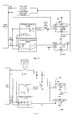
- Fig. 1 is a schematic view of an audio interface self-adaption device according to a first embodiment of the present disclosure.
- the audio interface self-adaption device of the embodiment comprises: an audio interface, a first level comparison module, a second level comparison module, a triode Tc, a power output terminal VBAT, a switching module, a resistor R2a, a resistor R2b, and so on.
- the first level comparison module comprises a triode Ta
- the second level comparison module comprises a triode Tb.
- the triode Ta is a NPN triode
- the triode Tb is a NPN triode
- the triode Tc is a PNP triode.
- a base (B) of the triode Ta is connected to the pin 4
- an emitter (E) of the triode Ta is connected to the pin 3
- a collector (C) of the triode Ta is connected to a base (B) of the triode Tc via the resistor R2a.
- the base (B) of the triode Ta may be connected to the pin 4 via a resistor R1a.
- a base (B) of the triode Tb is connected to the pin 3
- an emitter (E) of the triode Tb is connected to the pin 4
- a collector (C) of the triode Tb is connected to a signal input pin (Sel) of the switching module, and the collector (C) of the triode Tb is connected to the base (B) of the triode Tc via the resistor R2b.
- the base (B) of the triode Tb and the pin 3 may be connected via a resistor R1b.
- Each of the resistor R1a, the resistor R2a, the resistor R1b, and the resistor R2b has a resistance from 1K ⁇ to 1M ⁇ .
- An emitter (E) of the triode Tc is connected to the power output terminal VBAT, and a collector (C) of the triode Tc is connected to a power input pin (VCC) of the switching module.
- a voltage output by the power is generally from 2.7V to 4.2V.
- a B0L pin (may be called a first input pin) of the switching module is connected to the pin 4 of the audio interface
- a B1H pin (may be called a second input pin) of the switching module is connected to the pin 3 of the audio interface
- a ground pin (GND pin) of the switching module is connected to the ground
- a pin A (may be called an output pin) of the switching module is connected to the ground and to the pin 1 and the pin 2 of the audio interface.
- the pin 1 of the audio interface may be connected to a ground wire via a first signal processing module, and the pin 2 of the audio interface may be connected to the ground wire via a second signal processing module.
- Each of the first signal processing module and the second signal processing module may comprise at least one selected from a group consisting of: a resistor, a louder speaker, a transformer, and a signal processing module comprising a resistor and a comparator connected in parallel.
- a level V 3 of the pin 3 when a level V 3 of the pin 3 is greater than a sum of a level V 4 of the pin 4 and a predetermined threshold Vg (i.e. V 3 > V 4 +V g ), the triode Ta is in an OFF state, the triode Tb is in an ON state, and the triode Tc is in an ON state.
- the VBAT supplies power to the switching module via the VCC and a low level signal is received by the Sel pin of the switching module, which indicates the pin 3 is the MIC pin and the pin 4 is the GND pin.
- the triode Ta When the level V 4 of the pin 4 is greater than the sum of the level V 3 of the pin 3 and the predetermined threshold V g (i.e. V 4 > V 3 +V g ), the triode Ta is in an ON state, the triode Tb is in an OFF state, and the triode Tc is in an ON state.
- the VBAT supplies power to the switching module via the VCC and a high level signal is received by the Sel pin of the switching module, which indicates the pin 4 is the MIC pin and the pin 3 is the GND pin.
- the predetermined threshold V g is greater than or equal to 0.
- the threshold V g may be a breakover voltage of the triode Ta, such as 0.3V or 0.7V.
- the "high level signal” refers to a signal whose level is higher than the level of the above “low level signal”.
- the "low level signal” is a signal whose voltage is lower than 0.7V
- the "high level signal” is a signal whose voltage is higher than seventy percent of a voltage of the power, the definitions of which may also be applied to descriptions hereinafter.
- the switching module connects the B1H pin or the B0L pin to the pin A according to a signal received by the Sel pin, such that the pin 3 or the pin 4 of the audio interface is connected to the ground.
- the switching module When a low level signal is received by the Sel pin of the switching module, the switching module connects the B0L pin to the pin A, i.e. the B0L pin/ the pin 4 of the audio interface is connected to the ground.
- the switching module When a high level signal is received by the Sel pin of the switching module, the switching module connects the B1H pin to the pin A, i.e. the B1H pin/ the pin 3 of the audio interface is connected to the ground.
- Fig. 2 is a schematic view of an audio interface self-adaption device according to a second embodiment of the present disclosure. As shown in Fig.2 , the differences between the present embodiment and the Embodiment 1 are as follows.
- the pin 1 is connected to the pin 3 of the audio interface via a device having unidirectional conductivity (may be called a unidirectional conductive component, such as a diode, a triode, a MOS, and so on), the pin 1 is connected to the pin 4 of the audio interface via a device having unidirectional conductivity (may be called a unidirectional conductive component, such as a diode, a triode, a MOS, and so on), the pin 2 of the audio interface is connected to the pin 3 of the audio interface via a device having unidirectional conductivity (may be called a unidirectional conductive component such as a diode, a triode, a MOS, and so on), and the pin 2 of the audio interface is connected to the pin 4 of the audio interface via a device having unidirectional conductivity (may be called a unidirectional conductive component such as a diode, a triode, a MOS, and so on).
- a device having unidirectional conductivity may be called
- the pin 1 is connected to the pin 3 of the audio interface via a first signal processing module (such as a transformer U1) and a diode D1
- the pin 2 of the audio interface is connected to the pin 3 of the audio interface via a second signal processing module (such as a resistor R3) and the diode D1.
- the pin 1 is connected to the pin 4 of the audio interface via the first signal processing module (such as the transformer U1) and a diode D2
- the pin 2 is connected to the pin 4 of the audio interface via the second signal processing module (such as the resistor R3) and the diode D2.
- a resistance of the resistor R4 is greater than 1K ⁇ , and the resistance of the resistor R4 in the embodiment may be from 1K ⁇ to 20K ⁇ .
- the audio interface self-adaption device can be connected to an audio signal sending device with any type of audio interface, and pass a detection conducted by the audio signal sending device successfully.
- Fig. 3 is a schematic view of an audio interface self-adaption device according to a third embodiment of the present disclosure.
- the audio interface self-adaption device of the embodiment comprises: an audio interface, a first level comparison module, a second level comparison module, a triode Tc, a power output terminal VBAT, a switching module, a resistor R2a, a resistor R2b, and so on.
- the first level comparison module comprises a first reference voltage module H1 and a comparator C 1.
- the pin 3 is connected to a positive electrode of the comparator C1.
- the pin 4 is connected to a negative electrode of the comparator C1 via the first reference voltage module H1, i.e. the pin 4 is connected to a negative electrode of the first reference voltage module H1, and a positive electrode of the first reference voltage module H1 is connected to the negative electrode of the comparator C 1.
- the first reference voltage module H1 may be a power, and the power has a positive electrode being the positive electrode of the first reference voltage module H1 and a negative electrode being the negative electrode of the first reference voltage module H1.
- the voltage provided by the first reference voltage module H1 is a predetermined threshold Vg .
- the first reference voltage module H1 may be a component which can supply a reference voltage (the threshold voltage) such as a diode connected to the power.
- An output pin of the comparator C1 is connected to the base (B) of the triode Tc via the resistor R2a.
- the second level comparison module comprises a second reference voltage module H2 and a comparator C2.
- the pin 3 is connected to a negative electrode of the comparator C2.
- the pin 4 is connected to a positive electrode of the comparator C2 via the second reference voltage module H2, i.e. the pin 4 is connected to a positive electrode of the second reference voltage module H2, and a negative electrode of the second reference voltage module H2 is connected to the positive electrode of the comparator C2.
- the second reference voltage module H2 may be a power, and the power has a positive electrode being the positive electrode of the second reference voltage module H2 and a negative electrode being the negative electrode of the second reference voltage module H2.
- the voltage provided by the second reference voltage module H2 is the predetermined threshold V g .
- the second reference voltage module H2 may be a component which can supply a reference voltage (the threshold voltage) such as a diode connected to the power.
- An output pin of the comparator C2 is connected to a signal input pin (Sel) of the switching module, and the output pin of the comparator C2 is connected to the base (B) of the triode Tc via the resistor R2b.
- Each of the resistor R2a and the resistor R2b has a resistance from 1K ⁇ to 1M ⁇ .
- a B1H pin of the switching module is connected to the pin 3 of the audio interface
- a B0L pin of the switching module is connected to the pin 4 of the audio interface
- a ground pin (GND pin) of the switching module is connected to the ground (GND pin)
- a pin A of the switching module is connected to the ground, and the pin A is connected to the pin 1 and the pin 2 of the audio interface.
- the pin 1 of the audio interface may be connected to a ground wire via a first signal processing module, and the pin 2 of the audio interface may be connected to the ground wire via a second signal processing module.
- Each of the first signal processing module and the second signal processing module may comprise at least one selected from a group consisting of: a resistor, a louder speaker, a transformer, and a signal processing module comprising a resistor and a comparator connected in parallel.
- a level V 3 of the pin 3 is greater than a sum of the level V 4 of the pin 4 and a predetermined threshold Vg (i.e. V 3 > V 4 +V g )
- a high level signal is output by the comparator C1 of the first level comparison module
- a low level signal is output by the comparator C2 of the second level comparison module
- the triode Tc is in an ON state
- the VBAT supplies power to the switching module via the VCC
- a low level signal is received by the Sel pin of the switching module, which indicates the pin 3 is the MIC pin and the pin 4 is the GND pin.
- the level V 4 of the pin 4 is greater than the sum of the level V 3 of the pin 3 and the predetermined threshold V g (i.e. V 4 > V 3 +V g )
- a low level signal is output by the comparator C1 of the first level comparison module
- a high level signal is output by the comparator C2 of the second level comparison module
- the triode Tc is in an ON state
- the VBAT supplies power to the switching module via the VCC
- a high level signal is received by the Sel pin of the switching module, which indicates the pin 4 is the MIC pin and the pin 3 is the GND pin.
- the switching module connects the B1H pin or the B0L pin to the pin A according to the signal received by the Sel pin, such that the pin 3 or the pin 4 of the audio interface is connected to the ground.
- the switching module When a low level signal is received by the Sel pin of the switching module, the switching module connects the B0L pin to the pin A, i.e. the B0L pin/ the pin 4 of the audio interface is connected to the ground.
- the switching module When a high level signal is received by the Sel pin of the switching module, the switching module connects the B1H pin to the pin A, i.e. the B1H pin/ the pin 3 of the audio interface is connected to the ground.
- Fig. 4 is a schematic view of an audio interface self-adaption device according to a fourth embodiment of the present disclosure. As shown in Fig.4 , the differences between the present embodiment and the Embodiment 3 are as follows.
- the pin 1 of the audio interface is connected to the pin 3 of the audio interface via a device having unidirectional conductivity (referred as a unidirectional conductive component hereinafter, such as a diode, a triode, a MOS, and so on), the pin 1 of the audio interface is connected to the pin 4 of the audio interface via a device having unidirectional conductivity (referred as a unidirectional conductive component hereinafter, such as a diode, a triode, a MOS, and so on), the pin 2 of the audio interface is connected to the pin 3 of the audio interface via a device having unidirectional conductivity (referred as a unidirectional conductive component hereinafter, such as a diode, a triode, a MOS, and so on), and the pin 2 of the audio interface is connected to the pin 4 of the audio interface via a device having unidirectional conductivity (referred as a unidirectional conductive component hereinafter, such as a diode, a triode, a MOS, and
- the pin 1 of the audio interface is connected to the pin 3 of the audio interface via a diode D1
- the pin 2 of the audio interface is connected to the pin 3 of the audio interface via the diode D1
- the pin 1 of the audio interface is connected to the pin 4 of the audio interface via a diode D2
- the pin 2 of the audio interface is connected to the pin 4 of the audio interface via the diode D2.
- the resistance of the resistor R4 is greater than 1K ⁇ , and the resistance of the resistor R4 of the embodiment may be from 1K ⁇ to 20K ⁇ .
- the audio interface self-adaption device can be connected to an audio signal sending device with any type of audio interface, and pass a detection conducted by the audio signal sending device successfully.
- Fig. 5 is a schematic view of an audio interface self-adaption device according to a fifth embodiment of the present disclosure.
- the audio interface self-adaption device of the embodiment comprises: an audio interface, a first level comparison module, a second level comparison module, a PNP triode Tc, a power output terminal VBAT, a switching module, a resistor R2a, a resistor R2b, and so on.
- the first level comparison module comprises a NPN triode Ta.
- a base (B) of the triode Ta is connected to the pin 4
- an emitter (E) of the triode Ta is connected to the pin 3
- a collector (C) of the triode Ta is connected to a base (B) of the triode Tc via the resistor R2a.
- the base (B) of the triode Ta may be connected to the pin 4 via a resistor R1a.
- the second level comparison module comprises a second reference voltage module H2 and a comparator C2.
- the pin 3 is connected to a negative electrode of the comparator C2.
- the pin 4 is connected to a positive electrode of the comparator C2 via the second reference voltage module H2, i.e. the pin 4 is connected to a positive electrode of the second reference voltage module H2, and a negative electrode of the second reference voltage module H2 is connected to the positive electrode of the comparator C2.
- the second reference voltage module H2 may be a power, and the power has a positive electrode being the positive electrode of the second reference voltage module H2 and a negative electrode being the negative electrode of the second reference voltage module H2.
- the voltage provided by the second reference voltage module H2 is a predetermined threshold Vg .
- the second reference voltage module H2 may be a component which can supply a reference voltage (threshold voltage), such as a diode connected to a power.
- An output pin of the comparator C2 is connected to a signal input pin (Sel) of the switching module, and the output pin of the comparator C2 is connected to the base (B) of the triode Tc via the resistor R2b.
- Each of the resistor R2a and the resistor R2b has a resistance from 1K ⁇ to 1M ⁇ .
- a B1H pin of the switching module is connected to the pin 3 of the audio interface
- a B0L pin of the switching module is connected to the pin 4 of the audio interface
- a ground pin (GND pin) of the switching module is connected to the ground
- a pin A of the switching module is connected to the ground
- the pin A of the switching module is connected to the pin 1 and the pin 2 of the audio interface.
- the pin 1 of the audio interface may be connected to a ground wire via a first signal processing module, and the pin 2 of the audio interface may be connected to the ground wire via a second signal processing module.
- Each of the first signal processing module and the second signal processing module may comprise at least one selected from a group consisting of: a resistor, a louder speaker, a transformer, and a signal processing module comprising a resistor and a comparator connected in parallel.
- the triode Ta when a level V 3 of the pin 3 is greater than a sum of the level V 4 of the pin 4 and a threshold Vg (i.e. V 3 > V 4 +V g ), the triode Ta is in an OFF state, a low level signal is output by the comparator C2 of the second level comparison module, the triode Tc is in an ON state, the VBAT supplies power to the switching module via the VCC, and a low level signal is received by the Sel pin of the switching module, which indicates the pin 3 is the MIC pin and the pin 4 is the GND pin.
- Vg i.e. V 3 > V 4 +V g
- the triodes Ta When the level V 4 of the pin 4 is greater than the sum of the level V 3 of the pin 3 and the threshold V g (i.e. V 4 > V 3 +V g ), the triodes Ta is in an ON state, a high level signal is output by the comparator C2 of the second level comparison module, the triodes Tc is in an ON state, the VBAT supplies power to the switching module via the VCC, and a high level signal is received by the Sel pin of the switching module, which indicates the pin 4 is the MIC pin and the pin 3 is the GND pin.
- the threshold V g is greater than or equal to 0.
- the threshold V g may be a breakover voltage of the triode Ta, such as 0.3V or 0.7V.
- the switching module connects the B1H pin or the B0L pin to the pin A according to the signal received by the Sel pin, such that the pin 3 or the pin 4 of the audio interface is connected to the ground.
- the switching module When a low level signal is received by the Sel pin of the switching module, the switching module connects the B0L pin to the pin A, i.e. the B0L pin/ the pin 4 of the audio interface is connected to the ground.
- the switching module When a high level signal is received by the Sel pin of the switching module, the switching module connects the B1H pin to the pin A, i.e. the B1H pin/ the pin 3 of the audio interface is connected to the ground.
- Fig. 6 is a schematic view of an audio interface self-adaption device according to a sixth embodiment of the present disclosure. As shown in Fig.6 , the differences between the sixth embodiment and the fifth embodiment are as follows.
- the pin 1 of the audio interface is connected to the pin 3 of the audio interface via a device having unidirectional conductivity (referred as a unidirectional conductive component hereinafter, such as a diode, a triode, a MOS, and so on), the pin 1 of the audio interface is connected to the pin 4 of the audio interface via a device having unidirectional conductivity (referred as a unidirectional conductive component hereinafter, such as a diode, a triode, a MOS, and so on), the pin 2 of the audio interface is connected to the pin 3 of the audio interface via a device having unidirectional conductivity (referred as a unidirectional conductive component hereinafter, such as a diode, a triode, a MOS, and so on), and the pin 2 of the audio interface is connected to the pin 4 of the audio interface via a device having unidirectional conductivity (referred as a unidirectional conductive component hereinafter, such as a diode, a triode, a MOS, and
- the pin 1 of the audio interface is connected to the pin 3 of the audio interface via a diode D1
- the pin 2 of the audio interface is connected to the pin 3 of the audio interface via the diode D1
- the pin 1 of the audio interface is connected to the pin 4 of the audio interface via a diode D2
- the pin 2 of the audio interface is connected to the pin 4 of the audio interface via the diode D2.
- the resistance of the resistor R4 is greater than 1K ⁇ , and the resistance of the resistor R4 in the embodiment may be from 1K ⁇ to 20K ⁇ .
- the audio interface self-adaption device can be connected to an audio signal sending device with any type of audio interface, and pass a detection conducted by the audio signal sending device successfully.
- Fig. 7 is a schematic view of an audio interface self-adaption device according to a seventh embodiment of the present disclosure.
- the audio interface self-adaption device of the embodiment comprises: an audio interface, a first level comparison module, a second level comparison module, a PNP triode Tc, a power output terminal VBAT, a switching module, a resistor R2a, a resistor R2b, and so on.
- the first level comparison module comprises a first reference voltage module H1 and a comparator C 1.
- the pin 3 is connected to a positive electrode of the comparator C1.
- the pin 4 is connected to a negative electrode of the comparator C1 via the first reference voltage module H1, i.e. the pin 4 is connected to a negative electrode of the first reference voltage module H1, and a positive electrode of the first reference voltage module H1 is connected to the negative electrode of the comparator C 1.
- the first reference voltage module H1 may be a power, and the power has a positive electrode being the positive electrode of the first reference voltage module H1 and a negative electrode being the negative electrode of the first reference voltage module H1.
- the voltage provided by the first reference voltage module H1 is a threshold Vg .
- the first reference voltage module H1 may be a component which can supply a reference voltage (threshold voltage) such as a diode connected to the power.
- An output pin of the comparator C1 is connected to a base (B) of the triode Tc via the resistor R2a.
- the second level comparison module comprises a NPN triode Tb.
- a base (B) of the triode Tb is connected to the pin 3
- an emitter (E) of the triode Tb is connected to the pin 4
- a collector (C) of the triode Tb is connected to a signal input pin (Sel) of the switching module, and the collector (C) of the triode Tb is connected to the base (B) of the triode Tc via the resistor R2b.
- the base (B) of the triode Tb and the pin 3 may be connected via a resistor R1b.
- the voltage output by the power is generally from 2.7V to 4.2V.
- a B1H pin of the switching module is connected to the pin 3 of the audio interface
- a B0L pin of the switching module is connected to the pin 4 of the audio interface
- a ground pin (GND pin) of the switching module is connected to the ground
- a pin A of the switching module is connected to the ground
- the pin A of the switching module is connected to the pin 1 and the pin 2 of the audio interface.
- the pin 1 of the audio interface may be connected to a ground wire via a first signal processing module, and the pin 2 of the audio interface may be connected to the ground wire via a second signal processing module.
- Each of the first signal processing module and the second signal processing module may comprise at least one selected from a group consisting of: a resistor, a louder speaker, a transformer, and a signal processing module comprising a resistor and a comparator connected in parallel.
- the level V 3 of the pin 3 when the level V 3 of the pin 3 is greater than a sum of the level V 4 of the pin 4 and a predetermined threshold Vg (i.e. V 3 > V 4 +V g ), a high level signal is output by the comparator C1 of the first level comparison module, the triode Tb is in an ON state, the triode Tc is in an ON state, the VBAT supplies power to the switching module via the VCC, and a low level signal is received by the Sel pin of the switching module, which indicates the pin 3 is the MIC pin and the pin 4 is the GND pin.
- Vg i.e. V 3 > V 4 +V g
- the above predetermined threshold V g is greater than or equal to 0.
- the threshold V g may be a breakover voltage of the triode Ta, such as 0.3V or 0.7V.
- the switching module connects the B1H pin or the B0L pin to the pin A according to a signal received by the Sel pin, such that the pin 3 or the pin 4 of the audio interface is connected to the ground.
- the switching module When a low level signal is received by the Sel pin of the switching module, the switching module connects the B0L pin to the pin A, i.e. the B0L pin/ the pin 4 of the audio interface is connected to the ground.
- the switching module When a high level signal is received by the Sel pin of the switching module, the switching module connects the B1H pin to the pin A, i.e. the B1H pin/ the pin 3 of the audio interface is connected to the ground.
- Fig. 8 is a schematic view of an audio interface self-adaption device according to an eighth embodiment of the present disclosure. As shown in Fig.8 , the differences between the present embodiment and Embodiment 7 are as follows.
- the pin 1 of the audio interface is connected to the pin 3 of the audio interface via a unidirectional conductive component (such as a diode, a triode, a MOS, and so on), the pin 1 of the audio interface is connected to the pin 4 of the audio interface via a unidirectional conductive component (such as a diode, a triode, a MOS, and so on), the pin 2 of the audio interface is connected to the pin 3 of the audio interface via a unidirectional conductive component (such as a diode, a triode, a MOS, and so on), and the pin 2 of the audio interface is connected to the pin 4 of the audio interface via a unidirectional conductive component (such as a diode, a triode, a MOS, and so on).
- a unidirectional conductive component such as a diode, a triode, a MOS, and so on
- the pin 1 of the audio interface is connected to the pin 4 of the audio interface via a unidirectional
- the pin 1 of the audio interface is connected to the pin 3 of the audio interface via a diode D1
- the pin 2 of the audio interface is connected to the pin 3 of the audio interface via the diode D1
- the pin 1 of the audio interface is connected to the pin 4 of the audio interface via a diode D2
- the pin 2 of the audio interface is connected to the pin 4 of the audio interface via the diode D2.
- the resistance of the resistor R4 is greater than 1K ⁇ , and the resistance of the resistor R4 of the embodiment may be from 1K ⁇ to 20K ⁇ .
- the audio interface self-adaption device can be connected to an audio signal sending device with any type of audio interface, and pass a detection conducted by the audio signal sending device successfully.
- Fig. 9 is a schematic view of an audio interface self-adaption device according to a ninth embodiment of the present disclosure.
- the audio interface self-adaption device of the embodiment comprises: an audio interface, a first level comparison module, a second level comparison module, a power output terminal VBAT, a first switching module, a second switching module, and a resistor R2a, a resistor R2b, a resistor R3a, a resistor R3b, and so on.
- the first level comparison module comprises a triode Ta
- the second level comparison module comprises a triode Tb.
- the triode Ta is a NPN triode, and the triode Ta is a NPN triode.
- a base (B) of the triode Ta is connected to the pin 4
- an emitter (E) of the triode Ta is connected to the pin 3
- a collector (C) of the triode Ta is connected to the power output terminal VBAT via the resistor R2a and the resistor R3a
- the collector (C) of the triode Ta is connected to a signal input pin (Sell) of the first switching module via the resistor R2a.
- the base (B) of the triode Ta may be connected to the pin 4 via a resistor R1a.
- a base (B) of the triode Tb is connected to the pin 3
- an emitter (E) of the triode Tb is connected to the pin 4
- a collector (C) of the triode Tb is connected to the power output terminal VBAT via the resistor R2b and the resistor R3b
- the collector (C) of the triode Tb is connected to a signal input pin (Sel2) of the second switching module via the resistor R2b.
- the base (B) of the triode Tb and the pin 3 may be connected via a resistor R1b.
- Each of the resistor R1a, the resistor R2a, the resistor R1b, the resistor R2b, the resistor R3a, and the resistor R3b has a resistance from 1K ⁇ to 1M ⁇ .
- the voltage output by the power is generally from 2.7 to 4.2V.
- a B0L pin of the first switching module is connected to the pin 3 of the audio interface
- a B0L pin of the second switching module is connected to the pin 4 of the audio interface
- a ground pin (GND pin) of the first switching module is connected to the ground
- a ground pin (GND pin) of the second switching module is connected to the ground
- a pin A (may be called an output pin) of the first switching module is connected to the ground
- the pin A of the first switching module is connected to the pin 1 and the pin 2 of the audio interface
- a pin A (may be called an output pin) of the second switching module is connected to the ground
- the pin A of the second switching module is connected to the pin 1 and the pin 2 of the audio interface.
- the pin 1 of the audio interface may be connected to a ground wire via a first signal processing module, and the pin 2 of the audio interface may be connected to the ground wire via a second signal processing module.
- Each of the first signal processing module and the second signal processing module may comprise a resistor, a louder speaker, a transformer, and a signal processing module comprising a resistor and a comparator connected in parallel.
- a level V 3 of the pin 3 is greater than a sum of a level V 4 of the pin 4 and a predetermined threshold Vg (i.e. V 3 > V 4 +V g )
- the triode Ta is in an OFF state
- the triode Tb is in an ON state
- a low level signal is received by the Sel2 pin of the second switching module, which indicates the pin 3 is the MIC pin and the pin 4 is the GND pin.
- the triode Ta When the level V 4 of the pin 4 is greater than the sum of the level V 3 of the pin 3 and a predetermined threshold Vg (i.e. V 4 > V 3 +V g ), the triode Ta is in an ON state, the triode Tb is in an OFF state, a low level signal is received by the Sell pin of the first switching module, which indicates the pin 4 is the MIC pin and the pin 3 is the GND pin.
- Vg i.e. V 4 > V 3 +V g
- the predetermined threshold V g is greater than or equal to 0.
- the threshold V g may be a breakover voltage of the triode Ta, such as 0.3V or 0.7V.
- the above “high level signal” is a signal whose level is higher than a level of the above “low level signal”.
- the "low level signal” is a signal whose voltage is lower than 0.7V
- the “high level signal” is a signal whose voltage is higher than seventy percent of the supply voltage, the definitions of which may be applied to descriptions hereinafter.
- the second switching module connects the B0L pin to the pin A according to a low level signal received by the Sel2 pin, such that the pin 4 of the audio interface is connected to the ground.
- the second switching module When a low level signal is received by the Sel2 pin of the second switching module, the second switching module connects the B0L pin to the pin A, i.e. the B0L pin/ the pin 4 of the audio interface is connected to the ground.
- the first switching module connects the B0L pin to the pin A according to a low level signal received by the Sell pin, such that the pin 3 of the audio interface is connected to the ground.
- the first switching module When a low level signal is received by the Sell pin of the first switching module, the first switching module connects the B0L pin to the pin A, i.e. the B0L pin/ the pin 3 of the audio interface is connected to the ground.
- Fig. 10 is a schematic view of an audio interface self-adaption device according to a tenth embodiment of the present disclosure. As shown in Fig.10 , the differences between the present embodiment and Embodiment 9 are as follows.
- the pin 1 of the audio interface is connected to the pin 3 of the audio interface via a device having unidirectional conductivity (referred as a unidirectional conductive component hereinafter, such as a diode, a triode, a MOS, and so on), the pin 1 of the audio interface is connected to the pin 4 of the audio interface via a device having unidirectional conductivity (referred as a unidirectional conductive component hereinafter, such as a diode, a triode, a MOS, and so on), the pin 2 of the audio interface is connected to the pin 3 of the audio interface via a device having unidirectional conductivity (referred as a unidirectional conductive component hereinafter, such as a diode, a triode, a MOS, and so on), and the pin 2 of the audio interface is connected to the pin 4 of the audio interface via a device having unidirectional conductivity (referred as a unidirectional conductive component hereinafter, such as a diode, a triode, a MOS, and
- the pin 1 of the audio interface is connected to the pin 3 of the audio interface via a first signal processing module (such as a transformer U1) and a diode D1
- the pin 2 of the audio interface is connected to the pin 3 of the audio interface via a second signal processing module (such as a resistor R5) and the diode D1
- the pin 1 of the audio interface is connected to the pin 4 of the audio interface via a first signal processing module (such as the transformer U1) and a diode D2
- the pin 2 of the audio interface is connected to the pin 4 of the audio interface via a second signal processing module (such as the resistor R5) and the diode D2.
- the resistance of the resistor R4 is greater than 1K ⁇ , and the resistance of the resistor R4 of the embodiment may be from 1K ⁇ to 20K ⁇ .
- the audio interface self-adaption device can be connected to an audio signal sending device with any type of audio interface, and pass a detection conducted by the audio signal sending device successfully.
- Fig. 11 is a schematic view of an audio interface self-adaption device according to an eleventh embodiment of the present disclosure.
- the audio interface self-adaption device of the embodiment comprises: an audio interface, a first level comparison module, a second level comparison module, a power output terminal VBAT, a first switching module, a second switching module, and so on.
- the first level comparison module comprises a first reference voltage module H1 and a comparator C 1.
- the pin 3 is connected to a positive electrode of the comparator C1.
- the pin 4 is connected to a negative electrode of the comparator C1 via the first reference voltage module H1, i.e. the pin 4 is connected to a negative electrode of the first reference voltage module H1, and a positive electrode of the first reference voltage module H1 is connected to the negative electrode of the comparator C 1.
- the first reference voltage module H1 may be a power, and the power has a positive electrode being the positive electrode of the first reference voltage module H1 and a negative electrode being the negative electrode of the first reference voltage module H1.
- the voltage provided by the first reference voltage module H1 is a threshold Vg .
- the first reference voltage module H1 may be a component which can supply a reference voltage (threshold voltage) such as a diode connected to the power.
- An output pin of the comparator C1 is connected to a signal input pin (Sell) of the first switching module.
- the second level comparison module comprises a second reference voltage module H2 and a comparator C2.
- the pin 3 is connected to a negative electrode of the comparator C2.
- the pin 4 is connected to a positive electrode of the comparator C2 via the second reference voltage module H2, i.e. the pin 4 is connected to a positive electrode of the second reference voltage module H2, and a negative electrode of the second reference voltage module H2 is connected to the positive electrode of the comparator C2.
- the second reference voltage module H2 may be a power, and the power has a positive electrode being the positive electrode of the second reference voltage module H2 and a negative electrode being the negative electrode of the second reference voltage module H2.
- the voltage provided by the second reference voltage module H2 is the threshold Vg .
- the second reference voltage module H2 may be a component which can supply a reference voltage (threshold voltage), such as a diode connected to a power.
- An output pin of the comparator C2 is connected to a signal input pin (Sel2) of the second switching module.
- a B0L pin of the first switching module is connected to the pin 3 of the audio interface
- a B0L pin of the second switching module is connected to the pin 4 of the audio interface
- a ground pin (GND pin) of the first switching module is connected to the ground
- a ground pin (GND pin) of the second switching module is connected to the ground
- a pin A of the first switching module is connected to the ground
- the pin A of the first switching module is connected to the pin 1 and the pin 2 of the audio interface respectively
- a pin A of the second switching module is connected to the ground
- the pin A of the second switching module is connected to the pin 1 and the pin 2 of the audio interface respectively.
- the pin 1 of the audio interface may be connected to a ground wire via a first signal processing module, and the pin 2 of the audio interface may be connected to the ground wire via a second signal processing module.
- Each of the first signal processing module and the second signal processing module may comprise at least one selected from a group consisting of: a resistor, a louder speaker, a transformer, and a signal processing module comprising a resistor and a comparator connected in parallel.
- a level V 3 of the pin 3 is greater than a sum of a level V 4 of the pin 4 and a threshold Vg (i.e. V 3 > V 4 +V g )
- a high level signal is output by the comparator C1 of the first switching module
- a low level signal is output by the comparator C2 of the second switching module
- a low level signal is received by the Sel2 pin of the second switching module, which indicates the pin 3 is the MIC pin and the pin 4 is the GND pin.
- a low level signal is output by the comparator C1 of the first switching module, a high level signal is output by the comparator C2 of the second switching module, a low level signal is received by the Sell pin of the first switching module, which indicates the pin 4 is the MIC pin and the pin 3 is the GND pin.
- the first switching module connects the B0L pin to the pin A according to the low level signal received by the Sell pin, such that the pin 3 of the audio interface is connected to the ground.
- the first switching module When a low level signal is received by the Sell pin of the first switching module, the first switching module connects the B0L pin to the pin A, i.e. the B0L pin/ the pin 3 of the audio interface is connected to the ground.
- the second switching module connects the B0L pin to the pin A according to the low level signal received by the Sel2 pin, such that the pin 4 of the audio interface is connected to the ground.
- the second switching module When a low level signal is received by the Sel2 pin of the second switching module, the second switching module connects the B0L pin to the pin A, i.e. the B0L pin/ the pin 4 of the audio interface is connected to the ground.
- Fig. 12 is a schematic view of an audio interface self-adaption device according to a twelfth embodiment of the present disclosure. As shown in Fig.12 , the differences between the present embodiment and Embodiment 11 are as follows.
- the pin 1 of the audio interface is connected to the pin 3 of the audio interface via a unidirectional conductive component (such as a diode, a triode, a MOS, and so on), the pin 1 of the audio interface is connected to the pin 4 of the audio interface via a unidirectional conductive component (such as a diode, a triode, a MOS, and so on), the pin 2 of the audio interface is connected to the pin 3 of the audio interface via a unidirectional conductive component (such as a diode, a triode, a MOS, and so on), and the pin 2 of the audio interface is connected to the pin 4 of the audio interface via a unidirectional conductive component (such as a diode, a triode, a MOS, and so on).
- a unidirectional conductive component such as a diode, a triode, a MOS, and so on
- the pin 1 of the audio interface is connected to the pin 4 of the audio interface via a unidirectional
- the pin 1 of the audio interface is connected to the pin 3 of the audio interface via a diode D1
- the pin 2 of the audio interface is connected to the pin 3 of the audio interface via the diode D1
- the pin 1 of the audio interface is connected to the pin 4 of the audio interface via a diode D2
- the pin 2 of the audio interface is connected to the pin 4 of the audio interface via the diode D2.
- the resistance of the resistor R4 is greater than 1K ⁇ , and the resistance of the resistor R4 of the embodiment may be from 1K ⁇ to 20K ⁇ .
- the audio interface self-adaption device can be connected to an audio signal sending device with any type of audio interface, and pass a detection conducted by the audio signal sending device successfully.
- Fig. 13 is a schematic view of an audio interface self-adaption device according to a thirteenth embodiment of the present disclosure.
- the audio interface self-adaption device of the embodiment comprises: an audio interface, a first level comparison module, a second level comparison module, a power output terminal VBAT, a first switching module, a second switching module, a resistor R2a, a resistor R3a, and so on.
- the first level comparison module comprises a NPN triode Ta.
- a base (B) of the triode Ta is connected to the pin 4
- an emitter (E) of the triode Ta is connected to the pin 3
- a collector (C) of the triode Ta is connected to the power output terminal VBAT via the resistor R2a and the resistor R3a
- the collector (C) of the triode Ta is connected to a signal input pin (Sell) of the first switching module via the resistor R2a.
- the base (B) of the triode Ta may be connected to the pin 4 via a resistor R1a.
- the second level comparison module comprises a second reference voltage module H2 and a comparator C2.
- the pin 3 is connected to a negative electrode of the comparator C2.
- the pin 4 is connected to a positive electrode of the comparator C2 via the second reference voltage module H2, i.e. the pin 4 is connected to a positive electrode of the second reference voltage module H2, and a negative electrode of the second reference voltage module H2 is connected to the positive electrode of the comparator C2.
- the second reference voltage module H2 may be a power, and the power has a positive electrode being the positive electrode of the second reference voltage module H2 and a negative electrode being the negative electrode of the second reference voltage module H2.
- the voltage provided by the second reference voltage module H2 is a threshold Vg .
- the second reference voltage module H2 may be a component which can supply a reference voltage (threshold voltage), such as a diode connected to a power.
- An output pin of the comparator C2 is connected to a signal input pin (Sel2) of the second switching module.
- Each of the resistor R2a and the resistor R3a has a resistance from 1K ⁇ to 1M ⁇ .
- a B0L pin of the first switching module is connected to the pin 3 of the audio interface
- a B0L pin of the second switching module is connected to the pin 4 of the audio interface
- a ground pin (GND pin) of the first switching module is connected to the ground
- a ground pin (GND pin) of the second switching module is connected to the ground
- the ground pin (GND pin) of the first switching module is connected to the pin 1 and the pin 2 of the audio interface respectively
- the ground pin (GND pin) of the second switching module is connected to the pin 1 and the pin 2 of the audio interface respectively.
- the pin 1 of the audio interface may be connected to a ground wire via a first signal processing module, and the pin 2 of the audio interface may be connected to the ground wire via a second signal processing module.
- Each of the first signal processing module and the second signal processing module may comprise a resistor, a louder speaker, a transformer, and a signal processing module comprising resistor and comparator connected in parallel.
- a level V 3 of the pin 3 is greater than a sum of a level V 4 of the pin 4 and a threshold Vg (i.e. V 3 > V 4 +V g )
- the triode Ta is in an OFF state
- a low level signal is output by the comparator C2 of the second switching module
- a low level signal is received by the Sel2 pin of the second switching module, which indicates the pin 3 is the MIC pin and the pin 4 is the GND pin.
- the triode Ta When the level V 4 of the pin 4 is greater than the sum of the level V 3 of the pin 3 and the threshold Vg (i.e. V 4 > V 3 +V g ), the triode Ta is in an ON state, a high level signal is output by the comparator C2 of the second switching module, a low level signal is received by the Sell pin of the first switching module, which indicates the pin 4 is the MIC pin and the pin 3 is the GND pin.
- the threshold V g is greater than or equal to 0.
- the threshold V g may be a breakover voltage of the triode Ta, such as 0.3V or 0.7V
- the first switching module connects the B0L pin to the pin A according to the low level signal received by the Sell pin, such that the pin 3 of the audio interface is connected to the ground.
- the first switching module When a low level signal is received by the Sell pin of the first switching module, the first switching module connects the B0L pin to the pin A, i.e. the B0L pin/ the pin 3 of the audio interface is connected to the ground.
- the second switching module connects the B0L pin to the pin A according to the low level signal received by the Sel2 pin, such that the pin 4 of the audio interface is connected to the ground.
- the second switching module When a low level signal is received by the Sel2 pin of the second switching module, the second switching module connects the B0L pin to the pin A, i.e. the B0L pin/ the pin 4 of the audio interface is connected to the ground.
- Fig. 14 is a schematic view of an audio interface self-adaption device according to a fourteenth embodiment of the present disclosure. As shown in Fig. 14 , the differences between the present embodiment and the Embodiment 13 are as follows.
- the pin 1 of the audio interface is connected to the pin 3 of the audio interface via a device having unidirectional conductivity (referred as a unidirectional conductive component hereinafter, such as a diode, a triode, a MOS, and so on), the pin 1 of the audio interface is connected to the pin 4 of the audio interface via a device having unidirectional conductivity (referred as a unidirectional conductive component hereinafter, such as a diode, a triode, a MOS, and so on), the pin 2 of the audio interface is connected to the pin 3 of the audio interface via a device having unidirectional conductivity (referred as a unidirectional conductive component hereinafter, such as a diode, a triode, a MOS, and so on), and the pin 2 of the audio interface is connected to the pin 4 of the audio interface via a device having unidirectional conductivity (referred as a unidirectional conductive component hereinafter, such as a diode, a triode, a MOS, and
- the pin 1 of the audio interface is connected to the pin 3 of the audio interface via a diode D1
- the pin 2 of the audio interface is connected to the pin 3 of the audio interface via the diode D1
- the pin 1 of the audio interface is connected to the pin 4 of the audio interface via a diode D2
- the pin 2 of the audio interface is connected to the pin 4 of the audio interface via the diode D2.
- the resistance of the resistor R4 is greater than 1K ⁇ , and the resistance of the resistor R4 of the embodiment may be from 1K ⁇ to 20K ⁇ .
- the audio interface self-adaption device can be connected to an audio signal sending device with any type of audio interface, and pass a detection conducted by the audio signal sending device successfully.
- Fig. 15 is a schematic view of an audio interface self-adaption device according to a fifteenth embodiment of the present disclosure.
- the audio interface self-adaption device of the embodiment comprises: an audio interface, a first level comparison module, a second level comparison module, a power output terminal VBAT, a first switching module, a second switching module, resistor R2b, resistor R3b, and so on.
- the first level comparison module comprises a first reference voltage module H1 and a comparator C 1.
- the pin 3 is connected to a positive electrode of the comparator C1.
- the pin 4 is connected to a negative electrode of the comparator C1 via the first reference voltage module H1, i.e. the pin 4 is connected to a negative electrode of the first reference voltage module H1, and a positive electrode of the first reference voltage module H1 is connected to the negative electrode of the comparator C 1.
- the first reference voltage module H1 may be a power, and the power has a positive electrode being the positive electrode of the first reference voltage module H1 and a negative electrode being the negative electrode of the first reference voltage module H1.
- the voltage provided by the first reference voltage module H1 is a threshold Vg.
- the first reference voltage module H1 may be a component which can supply a reference voltage (threshold voltage), such as a diode connected to the power.
- An output pin of the comparator C1 is connected to a signal input pin (Sell) of the first switching module.
- the second level comparison module comprises a NPN triode Tb.
- a base (B) of the triode Tb is connected to the pin 3
- an emitter (E) of the triode Tb is connected to the pin 4
- a collector (C) of the triode Tb is connected to a signal input pin (Sel2) of the second switching module via the resistor R2b
- the collector (C) of the triode Tb is connected to the power output terminal VBAT via the resistor R2b and the resistor R3b.
- the base (B) of the triode Tb and the pin 3 may be connected via a resistor R1b.
- the voltage output by the power is generally from 2.7 to 4.2V.
- a B0L pin of the first switching module is connected to the pin 3 of the audio interface
- a B0L pin of the second switching module is connected to the pin 4 of the audio interface
- a ground pin (GND pin) of the first switching module is connected to the ground
- a ground pin (GND pin) of the second switching module is connected to the ground
- a pin A of the second switching module and is connected to the ground
- the pin A of the second switching module and is connected to the pin 1 and the pin 2 of the audio interface respectively.
- the pin 1 of the audio interface may be connected to a ground wire via a first signal processing module, and the pin 2 of that may be connected to the ground wire via a second signal processing module.
- Each of the first signal processing module and the second signal processing module may comprise at least one selected from a group consisting of: a resistor, a louder speaker, a transformer, and a signal processing module comprising a resistor and a comparator connected in parallel.
- a level V 3 of the pin 3 is greater than a sum of a level V 4 of the pin 4 and a predetermined threshold Vg (i.e. V 3 > V 4 +V g )
- a high level signal is output by the comparator C1 of the first switching module, the triode Tb is in an ON state, a low level signal is received by the Sel2 pin of the second switching module, which indicates the pin 3 is the MIC pin and the pin 4 is the GND pin.
- V 4 of the pin 4 When the level V 4 of the pin 4 is greater than the sum of the level V 3 of the pin 3 and a predetermined threshold V g (i.e. V 4 > V 3 +V g ), a low level signal is output by the comparator C1 of the first switching module, the triode Tb is in an OFF state, a low level signal is received by the Sell pin of the first switching module, which indicates the pin 4 is the MIC pin and the pin 3 is the GND pin.
- V g i.e. V 4 > V 3 +V g
- the predetermined threshold V g is greater than or equal to 0.
- the threshold V g may be a breakover voltage of the triode Ta, such as 0.3V or 0.7V
- the first switching module connects the B0L pin to the pin A according to the low level signal received by the Sell pin, such that the pin 3 of the audio interface is connected to the ground.
- the first switching module When a low level signal is received by the Sell pin of the first switching module, the first switching module connects the B0L pin to the pin A, i.e. the B0L pin/ the pin 3 of the audio interface is connected to the ground.
- the second switching module connects the B0L pin to the pin A according to the low level signal received by the Sel2 pin, such that the pin 4 of the audio interface is connected to the ground.
- the second switching module When a low level signal is received by the Sel2 pin of the second switching module, the second switching module connects the B0L pin to the pin A, i.e. the B0L pin/ the pin 4 of the audio interface is connected to the ground.
- Fig. 16 is a schematic view of an audio interface self-adaption device according to a sixteenth embodiment of the present disclosure. As shown in Fig.16 , the differences between the present embodiment and Embodiment 15 are as follows.
- the pin 1 of the audio interface is connected to the pin 3 of the audio interface via a unidirectional conductive component (such as a diode, a triode, a MOS, and so on), the pin 1 of the audio interface is connected to the pin 4 of the audio interface via a unidirectional conductive component (such as a diode, a triode, a MOS, and so on), the pin 2 of the audio interface is connected to the pin 3 of the audio interface via a unidirectional conductive component (such as a diode, a triode, a MOS, and so on), and the pin 2 of the audio interface is connected to the pin 4 of the audio interface via a unidirectional conductive component (such as a diode, a triode, a MOS, and so on).
- a unidirectional conductive component such as a diode, a triode, a MOS, and so on
- the pin 1 of the audio interface is connected to the pin 4 of the audio interface via a unidirectional
- the pin 1 of the audio interface is connected to the pin 3 of the audio interface via a diode D1
- the pin 2 of the audio interface is connected to the pin 3 of the audio interface via the diode D1
- the pin 1 of the audio interface is connected to the pin 4 of the audio interface via a diode D2
- the pin 2 of the audio interface is connected to the pin 4 of the audio interface via the diode D2.
- the resistance of the resistor R4 is greater than 1K ⁇ , and the resistance of the resistor R4 of the embodiment may be from 1K ⁇ to 20K ⁇ .
- the audio interface self-adaption device can be connected to an audio signal sending device with any type of audio interface, and pass a detection conducted by the audio signal sending device successfully.
- Fig. 17 is a schematic view of an audio interface self-adaption device according to a seventeenth embodiment of the present disclosure.
- the audio interface self-adaption device of the embodiment comprises: an audio interface, a level comparison module, a power output terminal VBAT, an earthed switching module, and so on.
- the level comparison module is configured to detect levels of the pin 3 and the pin 4 of the audio interface and to output a control instruction for controlling the earthed switching module according to the detected levels.
- the level comparison module comprises the first level comparison module and the second comparison module according to any of the Embodiments 1-16.
- the level comparison module of the embodiment may be a module which integrates all the functions of the first level comparison and the second comparison module.
- the power output terminal VBAT is configured to supply power for all modules. If an ordinary battery is used as the power, the voltage output by the power is generally from 2.7V to 4.2V.
- the earthed switching module is configured to connect a GND pin being the pin 3 or the pin 4 of the audio interface to the ground according to the control instruction output by the level comparison module.
- the earthed switching module comprises the switching module according to any of the Embodiments 1-8 and an external circuit (comprising a PNP triode Tc); or the earthed switching module comprises the first switching module and the second switching module according to any of the Embodiments 9-16.
- the pin 1 of the audio interface may be connected to a ground wire via a first signal processing module and the pin 2 of the audio interface may be connected to the ground wire via a second signal processing module.
- Each of the first signal processing module and the second signal processing module may comprise at least one selected from a group consisting of: a resistor, a louder speaker, a transformer, and a signal processing module comprising a resistor and a comparator connected in parallel.
- the level comparison module determines the level of the pin 3 is higher than the level of the pin 4 by comparing the levels of the pin 3 and the pin 4, which indicates the pin 4 is the GND pin, then the earthed switching module connects the pin 4 to the ground, and the earthed switching module connects the GND pin to a switching pin which is connected to the pin 4.
- the level comparison module determines the level of the pin 4 is higher than the level of the pin 3 by comparing levels of the pin 4 and the pin 3, which indicates the pin 3 is the GND pin, then the earthed switching module connects the pin 3 to the ground, and the earthed switching module connects the GND pin to the switching pin which is connected to the pin 3.
- the threshold V g is greater than or equal to 0.
- the threshold V g may be a breakover voltage of the triode Ta, such as 0.3V or 0.7V.
- Fig. 18 is a schematic view of an audio interface self-adaption device according to an eighteenth embodiment of the present disclosure. As shown in Fig.18 , the differences between the present embodiment and the Embodiment 17 are as follows.
- the pin 1 of the audio interface is connected to the pin 3 of the audio interface via a unidirectional conductive component (such as a diode, a triode, a MOS, and so on), the pin 1 of the audio interface is connected to the pin 4 of the audio interface via a unidirectional conductive component (such as a diode, a triode, a MOS, and so on), the pin 2 of the audio interface is connected to the pin 3 of the audio interface via a unidirectional conductive component (such as a diode, a triode, a MOS, and so on), and the pin 2 of the audio interface is connected to the pin 4 of the audio interface via a unidirectional conductive component (such as a diode, a triode, a MOS, and so on).
- a unidirectional conductive component such as a diode, a triode, a MOS, and so on
- the pin 1 of the audio interface is connected to the pin 4 of the audio interface via a unidirectional
- the pin 1 of the audio interface is connected to the pin 3 of the audio interface via a diode D1
- the pin 2 of the audio interface is connected to the pin 3 of the audio interface via the diode D1
- the pin 1 of the audio interface is connected to the pin 4 of the audio interface via a diode D2
- the pin 2 of the audio interface is connected to the pin 4 of the audio interface via the diode D2.
- the resistance of the resistor R4 is greater than 1K ⁇ , and the resistance of the resistor R4 of the embodiment may be from 1K ⁇ to 20K ⁇ .
- the audio interface self-adaption device can be connected to an audio signal sending device with any type of audio interface, and pass a detection conducted by the audio signal sending device successfully.
Landscapes
- Physics & Mathematics (AREA)
- Engineering & Computer Science (AREA)
- Acoustics & Sound (AREA)
- Signal Processing (AREA)
- Stereophonic Arrangements (AREA)
- Amplifiers (AREA)
- Circuit For Audible Band Transducer (AREA)
- Electrostatic, Electromagnetic, Magneto- Strictive, And Variable-Resistance Transducers (AREA)
Applications Claiming Priority (2)
| Application Number | Priority Date | Filing Date | Title |
|---|---|---|---|
| CN201210200188.5A CN102761803B (zh) | 2012-06-14 | 2012-06-14 | 一种音频接口自适应装置 |
| PCT/CN2013/077077 WO2013185592A1 (fr) | 2012-06-14 | 2013-06-14 | Dispositif d'auto-adaptation d'interface audio |
Publications (3)
| Publication Number | Publication Date |
|---|---|
| EP2863652A1 true EP2863652A1 (fr) | 2015-04-22 |
| EP2863652A4 EP2863652A4 (fr) | 2016-04-13 |
| EP2863652B1 EP2863652B1 (fr) | 2017-08-02 |
Family
ID=47056096
Family Applications (1)
| Application Number | Title | Priority Date | Filing Date |
|---|---|---|---|
| EP13804848.3A Not-in-force EP2863652B1 (fr) | 2012-06-14 | 2013-06-14 | Dispositif d'auto-adaptation d'interface audio |
Country Status (7)
| Country | Link |
|---|---|
| US (1) | US9407987B2 (fr) |
| EP (1) | EP2863652B1 (fr) |
| KR (1) | KR101519316B1 (fr) |
| CN (1) | CN102761803B (fr) |
| CA (1) | CA2876696C (fr) |
| SG (1) | SG11201408005VA (fr) |
| WO (1) | WO2013185592A1 (fr) |
Cited By (2)
| Publication number | Priority date | Publication date | Assignee | Title |
|---|---|---|---|---|
| CN106358119A (zh) * | 2016-09-20 | 2017-01-25 | 上海拓萧智能科技有限公司 | 一种音频适配器及其输出方法 |
| CN111263269A (zh) * | 2020-01-20 | 2020-06-09 | 广州市舒音电子科技有限公司 | 多功能话筒 |
Families Citing this family (13)
| Publication number | Priority date | Publication date | Assignee | Title |
|---|---|---|---|---|
| CN102761803B (zh) | 2012-06-14 | 2014-08-06 | 天地融科技股份有限公司 | 一种音频接口自适应装置 |
| CN202841070U (zh) * | 2012-06-28 | 2013-03-27 | 天地融科技股份有限公司 | 移动终端的音频接口匹配识别的装置及电子签名工具 |
| CN103052004A (zh) * | 2012-11-22 | 2013-04-17 | 北京小米科技有限责任公司 | 一种信号接收装置、耳机和转换接头 |
| GB2509316B (en) * | 2012-12-27 | 2015-02-25 | Wolfson Microelectronics Plc | Detection circuit |
| CN104038863A (zh) * | 2013-03-04 | 2014-09-10 | 上海城市地理信息系统发展有限公司 | 一种模拟耳机按键传输数据的方法和装置 |
| CN105704616A (zh) * | 2014-11-24 | 2016-06-22 | 天地融科技股份有限公司 | 通用音频适配装置及电子设备 |
| CN104507006B (zh) * | 2014-12-10 | 2018-03-20 | 天地融科技股份有限公司 | 音码产品及音码通信信道电路 |
| CN104640024A (zh) * | 2014-12-10 | 2015-05-20 | 天地融科技股份有限公司 | 音码产品及音码通信信道电路 |
| CN104735591B (zh) * | 2015-03-30 | 2018-09-28 | 天地融科技股份有限公司 | 音频接口适配电路与电子装置 |
| CN106331948A (zh) * | 2015-07-01 | 2017-01-11 | 朗新科技股份有限公司 | 具有自适配功能的手机音频接口通信设备 |
| CN106535037B (zh) * | 2015-09-10 | 2019-06-21 | 扬智科技股份有限公司 | 音效输出系统及其控制方法 |
| CN107979795A (zh) * | 2017-12-29 | 2018-05-01 | 数源科技股份有限公司 | 多音源智能侦测切换的音频切换器 |
| CN110166878B (zh) * | 2019-06-21 | 2020-08-07 | 昆腾微电子股份有限公司 | 耳机开关控制电路、耳机开关控制方法及电子设备 |
Family Cites Families (11)
| Publication number | Priority date | Publication date | Assignee | Title |
|---|---|---|---|---|
| JP4926005B2 (ja) * | 2007-11-13 | 2012-05-09 | ソニー・エリクソン・モバイルコミュニケーションズ株式会社 | 音声信号処理装置及び音声信号処理方法、通信端末 |
| EP2213085B1 (fr) * | 2007-11-21 | 2018-11-07 | Nokia Technologies Oy | Système de commutation d'interface de dispositif électronique |
| KR20090055359A (ko) | 2007-11-28 | 2009-06-02 | 삼성전자주식회사 | 4극 이어폰과 5극 이어폰 호환회로와 방법 및 이를이용하는 휴대 단말기 |
| US8223986B2 (en) * | 2009-11-19 | 2012-07-17 | Apple Inc. | Electronic device and external equipment with digital noise cancellation and digital audio path |
| CN101719610A (zh) * | 2009-12-30 | 2010-06-02 | 华为终端有限公司 | 一种有线耳机兼容方法和装置 |
| CN201797559U (zh) * | 2010-09-03 | 2011-04-13 | 深圳创维数字技术股份有限公司 | 能自动切换音频视频接口的机顶盒 |
| TWI505582B (zh) * | 2010-10-29 | 2015-10-21 | Fih Hong Kong Ltd | 耳機介面電路及具有該耳機介面電路之行動電話 |
| CN102300003B (zh) * | 2011-09-20 | 2013-12-11 | 惠州Tcl移动通信有限公司 | 一种自动检测耳机插口的移动终端 |
| EP2728899A4 (fr) | 2011-10-20 | 2014-09-03 | Huawei Device Co Ltd | Connecteur multifonctionnel pour multiplexage d'une interface de casque d'écoute en une interface vidéo et audio haute définition et dispositif électronique portatif |
| CN202721789U (zh) * | 2012-06-14 | 2013-02-06 | 天地融科技股份有限公司 | 一种音频接口自适应装置 |
| CN102761803B (zh) * | 2012-06-14 | 2014-08-06 | 天地融科技股份有限公司 | 一种音频接口自适应装置 |
-
2012
- 2012-06-14 CN CN201210200188.5A patent/CN102761803B/zh active Active
-
2013
- 2013-06-14 SG SG11201408005VA patent/SG11201408005VA/en unknown
- 2013-06-14 KR KR1020147036441A patent/KR101519316B1/ko not_active Expired - Fee Related
- 2013-06-14 US US14/407,529 patent/US9407987B2/en not_active Expired - Fee Related
- 2013-06-14 CA CA2876696A patent/CA2876696C/fr active Active
- 2013-06-14 EP EP13804848.3A patent/EP2863652B1/fr not_active Not-in-force
- 2013-06-14 WO PCT/CN2013/077077 patent/WO2013185592A1/fr not_active Ceased
Cited By (2)
| Publication number | Priority date | Publication date | Assignee | Title |
|---|---|---|---|---|
| CN106358119A (zh) * | 2016-09-20 | 2017-01-25 | 上海拓萧智能科技有限公司 | 一种音频适配器及其输出方法 |
| CN111263269A (zh) * | 2020-01-20 | 2020-06-09 | 广州市舒音电子科技有限公司 | 多功能话筒 |
Also Published As
| Publication number | Publication date |
|---|---|
| WO2013185592A1 (fr) | 2013-12-19 |
| EP2863652B1 (fr) | 2017-08-02 |
| US20150125005A1 (en) | 2015-05-07 |
| SG11201408005VA (en) | 2015-01-29 |
| CN102761803A (zh) | 2012-10-31 |
| KR101519316B1 (ko) | 2015-05-11 |
| CA2876696C (fr) | 2016-03-22 |
| CN102761803B (zh) | 2014-08-06 |
| KR20150020608A (ko) | 2015-02-26 |
| HK1178358A1 (en) | 2013-09-06 |
| US9407987B2 (en) | 2016-08-02 |
| CA2876696A1 (fr) | 2013-12-19 |
| EP2863652A4 (fr) | 2016-04-13 |
Similar Documents
| Publication | Publication Date | Title |
|---|---|---|
| EP2863652A1 (fr) | Dispositif d'auto-adaptation d'interface audio | |
| US9215541B2 (en) | Apparatus for detecting type of audio interface | |
| CN101841586B (zh) | 一种将手机耳机接口扩展为串口通信接口的方法 | |
| CN104035357B (zh) | 基于usb插座的耳机、充电和otg设备的电路设计 | |
| CN101102119B (zh) | 一种电器设备的充电检测电路及充电检测方法 | |
| CN103379420B (zh) | 一种确定耳机线序的方法及电子设备 | |
| CA2876716C (fr) | Procede et dispositif adaptatifs d'interface audio et jeton de signature electronique | |
| CN202721789U (zh) | 一种音频接口自适应装置 | |
| CN201075704Y (zh) | 一种电器设备的充电检测电路及具有所述电路的手机 | |
| CA2875380C (fr) | Procede, systeme et dispositif pour transmission de donnees audio et outil de signature electronique | |
| CN103197199A (zh) | 中断检测装置及方法 | |
| CN101917659A (zh) | 一种耳机电路的检测装置、方法及移动终端 | |
| CN204539442U (zh) | 音频接口适配电路与电子装置 | |
| CN204069293U (zh) | 蓝牙电路及包括该蓝牙电路的蓝牙装置 | |
| US20120056611A1 (en) | Connection detection circuit | |
| HK1178358B (en) | Self-adaptive device of audio interface | |
| EP3345405B1 (fr) | Compatibilité des microphones | |
| HK1185205B (en) | Device for detecting audio interface type |
Legal Events
| Date | Code | Title | Description |
|---|---|---|---|
| PUAI | Public reference made under article 153(3) epc to a published international application that has entered the european phase |
Free format text: ORIGINAL CODE: 0009012 |
|
| 17P | Request for examination filed |
Effective date: 20150109 |
|
| AK | Designated contracting states |
Kind code of ref document: A1 Designated state(s): AL AT BE BG CH CY CZ DE DK EE ES FI FR GB GR HR HU IE IS IT LI LT LU LV MC MK MT NL NO PL PT RO RS SE SI SK SM TR |
|
| AX | Request for extension of the european patent |
Extension state: BA ME |
|
| DAX | Request for extension of the european patent (deleted) | ||
| REG | Reference to a national code |
Ref country code: DE Ref legal event code: R079 Ref document number: 602013024498 Country of ref document: DE Free format text: PREVIOUS MAIN CLASS: H04R0003120000 Ipc: H04R0003000000 |
|
| RA4 | Supplementary search report drawn up and despatched (corrected) |
Effective date: 20160314 |
|
| RIC1 | Information provided on ipc code assigned before grant |
Ipc: H04R 5/04 20060101ALI20160308BHEP Ipc: H04R 3/00 20060101AFI20160308BHEP |
|
| GRAP | Despatch of communication of intention to grant a patent |
Free format text: ORIGINAL CODE: EPIDOSNIGR1 |
|
| INTG | Intention to grant announced |
Effective date: 20170105 |
|
| GRAS | Grant fee paid |
Free format text: ORIGINAL CODE: EPIDOSNIGR3 |
|
| GRAA | (expected) grant |
Free format text: ORIGINAL CODE: 0009210 |
|
| AK | Designated contracting states |
Kind code of ref document: B1 Designated state(s): AL AT BE BG CH CY CZ DE DK EE ES FI FR GB GR HR HU IE IS IT LI LT LU LV MC MK MT NL NO PL PT RO RS SE SI SK SM TR |
|
| REG | Reference to a national code |
Ref country code: CH Ref legal event code: EP Ref country code: AT Ref legal event code: REF Ref document number: 915655 Country of ref document: AT Kind code of ref document: T Effective date: 20170815 |
|
| REG | Reference to a national code |
Ref country code: IE Ref legal event code: FG4D |
|
| REG | Reference to a national code |
Ref country code: DE Ref legal event code: R096 Ref document number: 602013024498 Country of ref document: DE |
|
| REG | Reference to a national code |
Ref country code: NL Ref legal event code: MP Effective date: 20170802 |
|
| REG | Reference to a national code |
Ref country code: AT Ref legal event code: MK05 Ref document number: 915655 Country of ref document: AT Kind code of ref document: T Effective date: 20170802 |
|
| REG | Reference to a national code |
Ref country code: LT Ref legal event code: MG4D |
|
| PG25 | Lapsed in a contracting state [announced via postgrant information from national office to epo] |
Ref country code: NL Free format text: LAPSE BECAUSE OF FAILURE TO SUBMIT A TRANSLATION OF THE DESCRIPTION OR TO PAY THE FEE WITHIN THE PRESCRIBED TIME-LIMIT Effective date: 20170802 Ref country code: HR Free format text: LAPSE BECAUSE OF FAILURE TO SUBMIT A TRANSLATION OF THE DESCRIPTION OR TO PAY THE FEE WITHIN THE PRESCRIBED TIME-LIMIT Effective date: 20170802 Ref country code: FI Free format text: LAPSE BECAUSE OF FAILURE TO SUBMIT A TRANSLATION OF THE DESCRIPTION OR TO PAY THE FEE WITHIN THE PRESCRIBED TIME-LIMIT Effective date: 20170802 Ref country code: AT Free format text: LAPSE BECAUSE OF FAILURE TO SUBMIT A TRANSLATION OF THE DESCRIPTION OR TO PAY THE FEE WITHIN THE PRESCRIBED TIME-LIMIT Effective date: 20170802 Ref country code: NO Free format text: LAPSE BECAUSE OF FAILURE TO SUBMIT A TRANSLATION OF THE DESCRIPTION OR TO PAY THE FEE WITHIN THE PRESCRIBED TIME-LIMIT Effective date: 20171102 Ref country code: SE Free format text: LAPSE BECAUSE OF FAILURE TO SUBMIT A TRANSLATION OF THE DESCRIPTION OR TO PAY THE FEE WITHIN THE PRESCRIBED TIME-LIMIT Effective date: 20170802 Ref country code: LT Free format text: LAPSE BECAUSE OF FAILURE TO SUBMIT A TRANSLATION OF THE DESCRIPTION OR TO PAY THE FEE WITHIN THE PRESCRIBED TIME-LIMIT Effective date: 20170802 |
|
| PG25 | Lapsed in a contracting state [announced via postgrant information from national office to epo] |
Ref country code: RS Free format text: LAPSE BECAUSE OF FAILURE TO SUBMIT A TRANSLATION OF THE DESCRIPTION OR TO PAY THE FEE WITHIN THE PRESCRIBED TIME-LIMIT Effective date: 20170802 Ref country code: GR Free format text: LAPSE BECAUSE OF FAILURE TO SUBMIT A TRANSLATION OF THE DESCRIPTION OR TO PAY THE FEE WITHIN THE PRESCRIBED TIME-LIMIT Effective date: 20171103 Ref country code: IS Free format text: LAPSE BECAUSE OF FAILURE TO SUBMIT A TRANSLATION OF THE DESCRIPTION OR TO PAY THE FEE WITHIN THE PRESCRIBED TIME-LIMIT Effective date: 20171202 Ref country code: PL Free format text: LAPSE BECAUSE OF FAILURE TO SUBMIT A TRANSLATION OF THE DESCRIPTION OR TO PAY THE FEE WITHIN THE PRESCRIBED TIME-LIMIT Effective date: 20170802 Ref country code: LV Free format text: LAPSE BECAUSE OF FAILURE TO SUBMIT A TRANSLATION OF THE DESCRIPTION OR TO PAY THE FEE WITHIN THE PRESCRIBED TIME-LIMIT Effective date: 20170802 Ref country code: ES Free format text: LAPSE BECAUSE OF FAILURE TO SUBMIT A TRANSLATION OF THE DESCRIPTION OR TO PAY THE FEE WITHIN THE PRESCRIBED TIME-LIMIT Effective date: 20170802 Ref country code: BG Free format text: LAPSE BECAUSE OF FAILURE TO SUBMIT A TRANSLATION OF THE DESCRIPTION OR TO PAY THE FEE WITHIN THE PRESCRIBED TIME-LIMIT Effective date: 20171102 |
|
| PG25 | Lapsed in a contracting state [announced via postgrant information from national office to epo] |
Ref country code: CZ Free format text: LAPSE BECAUSE OF FAILURE TO SUBMIT A TRANSLATION OF THE DESCRIPTION OR TO PAY THE FEE WITHIN THE PRESCRIBED TIME-LIMIT Effective date: 20170802 Ref country code: DK Free format text: LAPSE BECAUSE OF FAILURE TO SUBMIT A TRANSLATION OF THE DESCRIPTION OR TO PAY THE FEE WITHIN THE PRESCRIBED TIME-LIMIT Effective date: 20170802 Ref country code: RO Free format text: LAPSE BECAUSE OF FAILURE TO SUBMIT A TRANSLATION OF THE DESCRIPTION OR TO PAY THE FEE WITHIN THE PRESCRIBED TIME-LIMIT Effective date: 20170802 |
|
| REG | Reference to a national code |
Ref country code: DE Ref legal event code: R097 Ref document number: 602013024498 Country of ref document: DE |
|
| PG25 | Lapsed in a contracting state [announced via postgrant information from national office to epo] |
Ref country code: EE Free format text: LAPSE BECAUSE OF FAILURE TO SUBMIT A TRANSLATION OF THE DESCRIPTION OR TO PAY THE FEE WITHIN THE PRESCRIBED TIME-LIMIT Effective date: 20170802 Ref country code: SM Free format text: LAPSE BECAUSE OF FAILURE TO SUBMIT A TRANSLATION OF THE DESCRIPTION OR TO PAY THE FEE WITHIN THE PRESCRIBED TIME-LIMIT Effective date: 20170802 Ref country code: IT Free format text: LAPSE BECAUSE OF FAILURE TO SUBMIT A TRANSLATION OF THE DESCRIPTION OR TO PAY THE FEE WITHIN THE PRESCRIBED TIME-LIMIT Effective date: 20170802 Ref country code: SK Free format text: LAPSE BECAUSE OF FAILURE TO SUBMIT A TRANSLATION OF THE DESCRIPTION OR TO PAY THE FEE WITHIN THE PRESCRIBED TIME-LIMIT Effective date: 20170802 |
|
| PLBE | No opposition filed within time limit |
Free format text: ORIGINAL CODE: 0009261 |
|
| STAA | Information on the status of an ep patent application or granted ep patent |
Free format text: STATUS: NO OPPOSITION FILED WITHIN TIME LIMIT |
|
| 26N | No opposition filed |
Effective date: 20180503 |
|
| PG25 | Lapsed in a contracting state [announced via postgrant information from national office to epo] |
Ref country code: SI Free format text: LAPSE BECAUSE OF FAILURE TO SUBMIT A TRANSLATION OF THE DESCRIPTION OR TO PAY THE FEE WITHIN THE PRESCRIBED TIME-LIMIT Effective date: 20170802 |
|
| REG | Reference to a national code |
Ref country code: CH Ref legal event code: PL |
|
| REG | Reference to a national code |
Ref country code: BE Ref legal event code: MM Effective date: 20180630 |
|
| REG | Reference to a national code |
Ref country code: IE Ref legal event code: MM4A |
|
| PG25 | Lapsed in a contracting state [announced via postgrant information from national office to epo] |
Ref country code: LU Free format text: LAPSE BECAUSE OF NON-PAYMENT OF DUE FEES Effective date: 20180614 Ref country code: MC Free format text: LAPSE BECAUSE OF FAILURE TO SUBMIT A TRANSLATION OF THE DESCRIPTION OR TO PAY THE FEE WITHIN THE PRESCRIBED TIME-LIMIT Effective date: 20170802 |
|
| PG25 | Lapsed in a contracting state [announced via postgrant information from national office to epo] |
Ref country code: CH Free format text: LAPSE BECAUSE OF NON-PAYMENT OF DUE FEES Effective date: 20180630 Ref country code: LI Free format text: LAPSE BECAUSE OF NON-PAYMENT OF DUE FEES Effective date: 20180630 Ref country code: FR Free format text: LAPSE BECAUSE OF NON-PAYMENT OF DUE FEES Effective date: 20180630 Ref country code: IE Free format text: LAPSE BECAUSE OF NON-PAYMENT OF DUE FEES Effective date: 20180614 |
|
| PG25 | Lapsed in a contracting state [announced via postgrant information from national office to epo] |
Ref country code: BE Free format text: LAPSE BECAUSE OF NON-PAYMENT OF DUE FEES Effective date: 20180630 |
|
| PG25 | Lapsed in a contracting state [announced via postgrant information from national office to epo] |
Ref country code: MT Free format text: LAPSE BECAUSE OF NON-PAYMENT OF DUE FEES Effective date: 20180614 |
|
| PG25 | Lapsed in a contracting state [announced via postgrant information from national office to epo] |
Ref country code: TR Free format text: LAPSE BECAUSE OF FAILURE TO SUBMIT A TRANSLATION OF THE DESCRIPTION OR TO PAY THE FEE WITHIN THE PRESCRIBED TIME-LIMIT Effective date: 20170802 |
|
| PG25 | Lapsed in a contracting state [announced via postgrant information from national office to epo] |
Ref country code: PT Free format text: LAPSE BECAUSE OF FAILURE TO SUBMIT A TRANSLATION OF THE DESCRIPTION OR TO PAY THE FEE WITHIN THE PRESCRIBED TIME-LIMIT Effective date: 20170802 |
|
| PG25 | Lapsed in a contracting state [announced via postgrant information from national office to epo] |
Ref country code: MK Free format text: LAPSE BECAUSE OF NON-PAYMENT OF DUE FEES Effective date: 20170802 Ref country code: HU Free format text: LAPSE BECAUSE OF FAILURE TO SUBMIT A TRANSLATION OF THE DESCRIPTION OR TO PAY THE FEE WITHIN THE PRESCRIBED TIME-LIMIT; INVALID AB INITIO Effective date: 20130614 Ref country code: CY Free format text: LAPSE BECAUSE OF FAILURE TO SUBMIT A TRANSLATION OF THE DESCRIPTION OR TO PAY THE FEE WITHIN THE PRESCRIBED TIME-LIMIT Effective date: 20170802 |
|
| PG25 | Lapsed in a contracting state [announced via postgrant information from national office to epo] |
Ref country code: AL Free format text: LAPSE BECAUSE OF FAILURE TO SUBMIT A TRANSLATION OF THE DESCRIPTION OR TO PAY THE FEE WITHIN THE PRESCRIBED TIME-LIMIT Effective date: 20170802 |
|
| PGFP | Annual fee paid to national office [announced via postgrant information from national office to epo] |
Ref country code: GB Payment date: 20220616 Year of fee payment: 10 Ref country code: DE Payment date: 20220607 Year of fee payment: 10 |
|
| REG | Reference to a national code |
Ref country code: DE Ref legal event code: R119 Ref document number: 602013024498 Country of ref document: DE |
|
| GBPC | Gb: european patent ceased through non-payment of renewal fee |
Effective date: 20230614 |
|
| PG25 | Lapsed in a contracting state [announced via postgrant information from national office to epo] |
Ref country code: DE Free format text: LAPSE BECAUSE OF NON-PAYMENT OF DUE FEES Effective date: 20240103 Ref country code: GB Free format text: LAPSE BECAUSE OF NON-PAYMENT OF DUE FEES Effective date: 20230614 |