EP2866232B1 - Transparente leitfähige folie und herstellungsverfahren dafür - Google Patents
Transparente leitfähige folie und herstellungsverfahren dafür Download PDFInfo
- Publication number
- EP2866232B1 EP2866232B1 EP13839469.7A EP13839469A EP2866232B1 EP 2866232 B1 EP2866232 B1 EP 2866232B1 EP 13839469 A EP13839469 A EP 13839469A EP 2866232 B1 EP2866232 B1 EP 2866232B1
- Authority
- EP
- European Patent Office
- Prior art keywords
- zno
- chemical formula
- conductive film
- transparent conductive
- inalo
- Prior art date
- Legal status (The legal status is an assumption and is not a legal conclusion. Google has not performed a legal analysis and makes no representation as to the accuracy of the status listed.)
- Active
Links
Images







Classifications
-
- C—CHEMISTRY; METALLURGY
- C01—INORGANIC CHEMISTRY
- C01G—COMPOUNDS CONTAINING METALS NOT COVERED BY SUBCLASSES C01D OR C01F
- C01G15/00—Compounds of gallium, indium or thallium
- C01G15/006—Compounds containing gallium, indium or thallium, with or without oxygen or hydrogen, and containing two or more other elements
-
- H—ELECTRICITY
- H01—ELECTRIC ELEMENTS
- H01B—CABLES; CONDUCTORS; INSULATORS; SELECTION OF MATERIALS FOR THEIR CONDUCTIVE, INSULATING OR DIELECTRIC PROPERTIES
- H01B1/00—Conductors or conductive bodies characterised by the conductive materials; Selection of materials as conductors
- H01B1/06—Conductors or conductive bodies characterised by the conductive materials; Selection of materials as conductors mainly consisting of other non-metallic substances
- H01B1/08—Conductors or conductive bodies characterised by the conductive materials; Selection of materials as conductors mainly consisting of other non-metallic substances oxides
-
- H—ELECTRICITY
- H01—ELECTRIC ELEMENTS
- H01B—CABLES; CONDUCTORS; INSULATORS; SELECTION OF MATERIALS FOR THEIR CONDUCTIVE, INSULATING OR DIELECTRIC PROPERTIES
- H01B13/00—Apparatus or processes specially adapted for manufacturing conductors or cables
-
- H—ELECTRICITY
- H01—ELECTRIC ELEMENTS
- H01B—CABLES; CONDUCTORS; INSULATORS; SELECTION OF MATERIALS FOR THEIR CONDUCTIVE, INSULATING OR DIELECTRIC PROPERTIES
- H01B5/00—Non-insulated conductors or conductive bodies characterised by their form
- H01B5/14—Non-insulated conductors or conductive bodies characterised by their form comprising conductive layers or films on insulating-supports
-
- H—ELECTRICITY
- H10—SEMICONDUCTOR DEVICES; ELECTRIC SOLID-STATE DEVICES NOT OTHERWISE PROVIDED FOR
- H10D—INORGANIC ELECTRIC SEMICONDUCTOR DEVICES
- H10D30/00—Field-effect transistors [FET]
- H10D30/60—Insulated-gate field-effect transistors [IGFET]
- H10D30/67—Thin-film transistors [TFT]
- H10D30/6729—Thin-film transistors [TFT] characterised by the electrodes
- H10D30/6737—Thin-film transistors [TFT] characterised by the electrodes characterised by the electrode materials
- H10D30/6739—Conductor-insulator-semiconductor electrodes
-
- H—ELECTRICITY
- H10—SEMICONDUCTOR DEVICES; ELECTRIC SOLID-STATE DEVICES NOT OTHERWISE PROVIDED FOR
- H10D—INORGANIC ELECTRIC SEMICONDUCTOR DEVICES
- H10D30/00—Field-effect transistors [FET]
- H10D30/60—Insulated-gate field-effect transistors [IGFET]
- H10D30/67—Thin-film transistors [TFT]
- H10D30/674—Thin-film transistors [TFT] characterised by the active materials
- H10D30/6755—Oxide semiconductors, e.g. zinc oxide, copper aluminium oxide or cadmium stannate
-
- H—ELECTRICITY
- H10—SEMICONDUCTOR DEVICES; ELECTRIC SOLID-STATE DEVICES NOT OTHERWISE PROVIDED FOR
- H10D—INORGANIC ELECTRIC SEMICONDUCTOR DEVICES
- H10D30/00—Field-effect transistors [FET]
- H10D30/60—Insulated-gate field-effect transistors [IGFET]
- H10D30/67—Thin-film transistors [TFT]
- H10D30/6757—Thin-film transistors [TFT] characterised by the structure of the channel, e.g. transverse or longitudinal shape or doping profile
-
- H—ELECTRICITY
- H10—SEMICONDUCTOR DEVICES; ELECTRIC SOLID-STATE DEVICES NOT OTHERWISE PROVIDED FOR
- H10D—INORGANIC ELECTRIC SEMICONDUCTOR DEVICES
- H10D64/00—Electrodes of devices having potential barriers
- H10D64/60—Electrodes characterised by their materials
- H10D64/62—Electrodes ohmically coupled to a semiconductor
-
- H—ELECTRICITY
- H10—SEMICONDUCTOR DEVICES; ELECTRIC SOLID-STATE DEVICES NOT OTHERWISE PROVIDED FOR
- H10D—INORGANIC ELECTRIC SEMICONDUCTOR DEVICES
- H10D64/00—Electrodes of devices having potential barriers
- H10D64/60—Electrodes characterised by their materials
- H10D64/66—Electrodes having a conductor capacitively coupled to a semiconductor by an insulator, e.g. MIS electrodes
- H10D64/667—Electrodes having a conductor capacitively coupled to a semiconductor by an insulator, e.g. MIS electrodes the conductor comprising a layer of alloy material, compound material or organic material contacting the insulator, e.g. TiN workfunction layers
-
- H—ELECTRICITY
- H10—SEMICONDUCTOR DEVICES; ELECTRIC SOLID-STATE DEVICES NOT OTHERWISE PROVIDED FOR
- H10D—INORGANIC ELECTRIC SEMICONDUCTOR DEVICES
- H10D64/00—Electrodes of devices having potential barriers
- H10D64/60—Electrodes characterised by their materials
- H10D64/66—Electrodes having a conductor capacitively coupled to a semiconductor by an insulator, e.g. MIS electrodes
- H10D64/68—Electrodes having a conductor capacitively coupled to a semiconductor by an insulator, e.g. MIS electrodes characterised by the insulator, e.g. by the gate insulator
- H10D64/691—Electrodes having a conductor capacitively coupled to a semiconductor by an insulator, e.g. MIS electrodes characterised by the insulator, e.g. by the gate insulator comprising metallic compounds, e.g. metal oxides or metal silicates
-
- H—ELECTRICITY
- H10—SEMICONDUCTOR DEVICES; ELECTRIC SOLID-STATE DEVICES NOT OTHERWISE PROVIDED FOR
- H10F—INORGANIC SEMICONDUCTOR DEVICES SENSITIVE TO INFRARED RADIATION, LIGHT, ELECTROMAGNETIC RADIATION OF SHORTER WAVELENGTH OR CORPUSCULAR RADIATION
- H10F77/00—Constructional details of devices covered by this subclass
- H10F77/20—Electrodes
- H10F77/244—Electrodes made of transparent conductive layers, e.g. transparent conductive oxide [TCO] layers
-
- H—ELECTRICITY
- H10—SEMICONDUCTOR DEVICES; ELECTRIC SOLID-STATE DEVICES NOT OTHERWISE PROVIDED FOR
- H10K—ORGANIC ELECTRIC SOLID-STATE DEVICES
- H10K30/00—Organic devices sensitive to infrared radiation, light, electromagnetic radiation of shorter wavelength or corpuscular radiation
- H10K30/80—Constructional details
- H10K30/81—Electrodes
- H10K30/82—Transparent electrodes, e.g. indium tin oxide [ITO] electrodes
-
- C—CHEMISTRY; METALLURGY
- C01—INORGANIC CHEMISTRY
- C01P—INDEXING SCHEME RELATING TO STRUCTURAL AND PHYSICAL ASPECTS OF SOLID INORGANIC COMPOUNDS
- C01P2002/00—Crystal-structural characteristics
- C01P2002/70—Crystal-structural characteristics defined by measured X-ray, neutron or electron diffraction data
- C01P2002/76—Crystal-structural characteristics defined by measured X-ray, neutron or electron diffraction data by a space-group or by other symmetry indications
-
- C—CHEMISTRY; METALLURGY
- C01—INORGANIC CHEMISTRY
- C01P—INDEXING SCHEME RELATING TO STRUCTURAL AND PHYSICAL ASPECTS OF SOLID INORGANIC COMPOUNDS
- C01P2002/00—Crystal-structural characteristics
- C01P2002/70—Crystal-structural characteristics defined by measured X-ray, neutron or electron diffraction data
- C01P2002/77—Crystal-structural characteristics defined by measured X-ray, neutron or electron diffraction data by unit-cell parameters, atom positions or structure diagrams
-
- C—CHEMISTRY; METALLURGY
- C01—INORGANIC CHEMISTRY
- C01P—INDEXING SCHEME RELATING TO STRUCTURAL AND PHYSICAL ASPECTS OF SOLID INORGANIC COMPOUNDS
- C01P2006/00—Physical properties of inorganic compounds
- C01P2006/40—Electric properties
-
- H—ELECTRICITY
- H10—SEMICONDUCTOR DEVICES; ELECTRIC SOLID-STATE DEVICES NOT OTHERWISE PROVIDED FOR
- H10K—ORGANIC ELECTRIC SOLID-STATE DEVICES
- H10K50/00—Organic light-emitting devices
- H10K50/80—Constructional details
- H10K50/805—Electrodes
- H10K50/81—Anodes
-
- Y—GENERAL TAGGING OF NEW TECHNOLOGICAL DEVELOPMENTS; GENERAL TAGGING OF CROSS-SECTIONAL TECHNOLOGIES SPANNING OVER SEVERAL SECTIONS OF THE IPC; TECHNICAL SUBJECTS COVERED BY FORMER USPC CROSS-REFERENCE ART COLLECTIONS [XRACs] AND DIGESTS
- Y02—TECHNOLOGIES OR APPLICATIONS FOR MITIGATION OR ADAPTATION AGAINST CLIMATE CHANGE
- Y02E—REDUCTION OF GREENHOUSE GAS [GHG] EMISSIONS, RELATED TO ENERGY GENERATION, TRANSMISSION OR DISTRIBUTION
- Y02E10/00—Energy generation through renewable energy sources
- Y02E10/50—Photovoltaic [PV] energy
- Y02E10/549—Organic PV cells
-
- Y—GENERAL TAGGING OF NEW TECHNOLOGICAL DEVELOPMENTS; GENERAL TAGGING OF CROSS-SECTIONAL TECHNOLOGIES SPANNING OVER SEVERAL SECTIONS OF THE IPC; TECHNICAL SUBJECTS COVERED BY FORMER USPC CROSS-REFERENCE ART COLLECTIONS [XRACs] AND DIGESTS
- Y02—TECHNOLOGIES OR APPLICATIONS FOR MITIGATION OR ADAPTATION AGAINST CLIMATE CHANGE
- Y02P—CLIMATE CHANGE MITIGATION TECHNOLOGIES IN THE PRODUCTION OR PROCESSING OF GOODS
- Y02P70/00—Climate change mitigation technologies in the production process for final industrial or consumer products
- Y02P70/50—Manufacturing or production processes characterised by the final manufactured product
Definitions
- the present invention relates to a transparent conductive film and a method for preparing the same.
- a transparent conductive film refers to a thin film having high light transmittance and an electrically conductive property and has been widely used as a voltage apply type common electrode or pixel electrode of a liquid crystal display, an electrochromic display (ECD, an organic electroluminescence device, a solar cell, a plasma display panel, a flexible display, electronic paper, a touch panel, and the like.
- ECD electrochromic display
- OLED organic electroluminescence device
- solar cell a plasma display panel
- a flexible display electronic paper, a touch panel, and the like.
- TCOs transparent conducting oxides
- an electronic energy band gap needs to be 3.1 eV or more equivalent to electromagnetic wave energy having a wavelength of 400 nm.
- the TCO has light transmittance of 80% or more in the visible ray area and specific resistance of about 10 -4 ⁇ cm or less as an electrical property.
- In 2 O 3 has the specific resistance lower than that of SnO 2 or ZnO, and, thus, it was the first to be commercialized.
- ITO Tin doped In 2 O 3
- the ITO is a material having been used for an electrode for display in an LED, an LCD, a PDP, etc., a solar cell, and the like and has the low specific resistance of 10 -4 ⁇ cm in general or 10 -5 ⁇ cm in lab-scale which is close to specific resistance of metal.
- the ITO has the disadvantage of high price since In is one of rare elements, and if it is exposed to hydrogen plasma often used in a flat panel display manufacturing process, In or Sn is reduced and electrical and optical properties may be deteriorated. Further, it is known that the ITO is an n -type semiconductor and cannot be converted into a p- type semiconductor. For this reason, it is impossible to constitute a homo junction circuit element with the ITO only.
- US2011/177696 A1 discloses a crystalline structure comprising InAlZnO 4 or InAlO 3 (ZnO) 2 crystal. These crystals may be used as a sputtering target for manufacturing conductive films.
- a transparent conductive film comprising a compound having a crystalline structure and represented by Chemical Formula 1, wherein the compound represented by Chemical Formula 1 is additionally doped with an n-type dopant, and wherein the n-type dopant comprises at least one selected from the group consisting of Sn, Ge, and Mo: [Chemical Formula 1] [(R p X q )O 3 ] m (AO) n where,
- a method for preparing a transparent conductive film comprising forming, on a substrate, a compound having a crystalline structure and represented by Chemical Formula 1 wherein the forming a compound represented by Chemical Formula 1 uses a DC/RF magnetron sputtering method or a molecular beam epitaxy method, wherein the compound represented by Chemical Formula 1 is additionally doped with an n-type dopant, and wherein the n-type dopant comprises at least one selected from the group consisting of Sn, Ge, and Mo: [Chemical Formula 1] [(R p X q )O 3 ] m (AO) n where,
- an electronic element comprising the transparent conductive film.
- a thin film transistor comprising the transparent conductive film. Further embodiments are disclosed in the sub-claims.
- a transparent conductive film according to an exemplary embodiment of the present application comprises a compound having a crystalline structure and represented by Chemical Formula 1 and thus has excellent conductivity and transmittance. Further, the transparent conductive film according to an exemplary embodiment of the present application has excellent elasticity and adhesive strength. Furthermore, the transparent conductive film according to an exemplary embodiment of the present application has a low haze value. Therefore, the transparent conductive film according to the present application can be applied as a technology substituting for conventional ITO conductive films.
- the present application can be applied to next-generation flexible devices, transparent AMOLED, OLED lighting, and solar cells as well as the industry of flat panel display devices such as LCD, PDP, and the like.
- a transparent oxide semiconductor is very important as a key technolgy of the transparent electronics technolgoy because the use of materials such as ITO (Sn-doped In 2 O 3 ) and ZnO used as trnaprent electrodes of conventioanl optoelectronic devices is really considerable.
- ITO Tin-doped In 2 O 3
- ZnO used as trnaprent electrodes of conventioanl optoelectronic devices
- ITO or AZO Al-doped ZnO
- ITO or AZO Al-doped ZnO
- AZO Al-doped ZnO
- Such materials have high electrical conductivity and high transission of photon and also have a metal s -orbial that exhibits spatial delocalization of a conduction band, and low energy, low effecitve mass, as an electronic structural property in common to n -type TCO materials.
- cations such as Zn(II), Ga(III), and In(III) in a closed-shell n s 0 state are bonded to oxides.
- Ga-doped ZnO or F-doped SnO 2 has been known as a TCO material. It is known that thses materilas have a carrier concentration (N(cm -3 )) of 10 16 to 10 21 and an electron mobility ( ⁇ (cm 2 V -1 s -1 )) of about 10 to about 1,000.
- valence band state exhibits a localized O 2p state.
- Such a deep localized state involves local lattaic distortion, resulting in formation of a small polaron (a quasiparticle derived from an electric charge or an electric field).
- a hole conducting p -type TCO material has a structure which can transmit a hole since a metal such as Cu(I) has a low bond energy at a valence band maximum (VBM).
- VBM valence band maximum
- its hole mobility is as low as less than 10 cm 2 V -1 s -1 due to an effect of a d band of localized metal such as Cu and existence of an indirect band gap.
- TCOs having various strucutres As a new TCO material candidate, a ternary compound and binary compound such as ZnO-In 2 O 3 -SnO 2 system, ZnO-In 2 O 3 (IZO), and the like have been researched. However, we need to take note of TCO materials having more physicochemically stable and electrically and optically excellent properties.
- DFT density functional theory
- the final technical objective of such materials used in the transparent electronics is how to manufacure a transparent homo junction. Since all of the conventional transparent electrodes or devices use hetero junction, an electro rectifying voltage is low and an electrical mobility of the hetero junction is inferior to that of the homo junction. Therefore, the ultimate method to solve such a problem is to find a semiconductor material which can be bipolar doped.
- a transparent conductive film comprises a compound having a crystalline structure and represented by Chemical Formula 1, wherein the compound represented by Chemical Formula 1 is additionally doped with an n-type dopant, and wherein the n-type dopant comprises at least one selected from the group consisting of Sn, Ge, and Mo: [Chemical Formula 1] [(R p X q )O 3 ] m (AO) n where,
- the A of Chemical Formula 1 may be Zn but may not be limited thereto.
- the compound represented by Chemical Formula 1 may be InAlO 3 (ZnO) n , and the n may be 1 to 7 but may not be limited thereto.
- the compound may have a rhomohedral ( R 3 m ) strucutre, and if the n is an even number, the compound may have a hexagonal polymorph ( P6 3 / mmc ) structure.
- the compound represented by Chemical Formula 1 has a crystalline structure. As described above, since the compound represented by Chemical Formula 1 has a crystalline structure, it can satisfy transparency, conductivity, etc. as required in the art. Further, by additionally doping the compound represented by Chemical Formula 1 with an n-type dopant, a p-type dopant, etc., if necessary, transparency and elctrical properties of the compound represented by Chemical Formula 1 can be regulated.
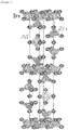
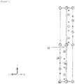
- FIG 1 a structure of InAlO 3 (ZnO) 4 is illustrated in FIG 1 .
- FIG 2 A structure of InGaO 3 (ZnO) 4 is illustrated in FIG 2 .
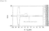
- DOS Density of State
- nAlO 3 (ZnO) 4 and InGaO 3 (ZnO) 4 are illustrated in FIGS. 3 and 5 , respectively
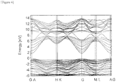
- band structures of the nAlO 3 (ZnO) 4 and InGaO 3 (ZnO) 4 are illustrated in FIGS. 4 and 6 , respectively.
- VBM valence band maximum
- CBM conduction band minimum
- the band structure exhibits energy levels of electrons at lattice points in a reciprocal space, and "0" on the vertical axis refers to Fermi energy.
- a valence band refers to bands lower than the Fermi energy and a conduction band refers to bands higher than the Fermi energy.
- a reciprocal number of a second derivative with respect to the reciprocal space having the horizontal aixs of bands refers to an effective mass of an electron
- an example material of the present application has a high curvature of the conduction band with reference to a G point (gamma point).
- LuFeO 3 (ZnO) n (n: 1, 4, 5, or 6) is illustrated in FIG. 9 .
- FIG. 9 illustrates a case where the n is 1, (b) illustrates case where the n is 4, (c) illustrates a case where the n is 5, (d) illustrates a case where the n is 6, and (e) illustrates a structure of ZnO.
- the compound of Chemical Formula 1 is doped with an additional element.
- the compound represented by Chemical Formula 1 is additionally doped with an n-type dopant.
- the n-type dopant comprises at least one selected from the group consisting of Sn, Ge, and Mo.
- InAlSnO 3 (ZnO) 4 obtained by additionally doping the InAlO 3 (ZnO) 4 with Sn, a mobility may be increased as compared with the InAlO 3 (ZnO) 4 ( ⁇ 10 cm2/Vsec).
- the compound represented by Chemical Formula 1 may be additionally doped with a p-type dopant.
- the p-type dopant may be a nitrogen atom but may not be limited thereto.
- N-doped InAlO 3 (ZnO) 4 As a compound obtained by additionally doping the compound represented by Chemical Formula 1 with a p-type dopant, there is an N-doped InAlO 3 (ZnO) 4 .
- the N-doped InAlO 3 (ZnO) 4 may be represented by InAlO 3 (ZnO) 4 :N.
- FIG. 10 A density of state of the N-doped InAlO 3 (ZnO) 4 is illustrated in FIG. 10 , and a structure of the N-doped InAlO 3 (ZnO) 4 is illustrated in FIG. 11 .
- a p-orbital component of N doping an O-site exhibits a p-type characteristic illustrated right above a VBM.
- a content range of an element in the compound of Chemical Formula 1, a content range of an additional doping element, etc. can be regulated in various ways to be suitable for purpose.
- an electronic element comprising the transparent conductive film.
- the transparent conductive film according to the present application can be used as a common electrode or pixel electrode of a liquid crystal display, an electrochromic display (ECD, an organic electroluminescence device, a solar cell, a plasma display panel, a flexible display, electronic paper, a touch panel, and the like.
- ECD electrochromic display
- organic electroluminescence device a solar cell
- plasma display panel a flexible display
- electronic paper a touch panel, and the like.
- a thin film transistor comprising the transparent conductive film.
- the transparent conductive film according to the present application can be used as a source electrode, a drain electrode, and a gate electrode of a thin film transistor and also used as an active layer and a gate insulating layer. That is, any one of the components of the thin film transistor can be formed of the transparent conductive film according to the present application or all of the components of the thin film transistor can be formed of the transparent conductive film according to the present application. Accordingly, a circuit of a smart window can be formed.
- FIG. 12 A structure of a thin film transistor according to the present application is illustrated in FIG. 12 .
- FIG. 12 schematically illustrates a thin film transistor employing InAlO 3 (ZnO) 4 and InGaO 3 (ZnO) 4 .
- the thin film transistor may comprise a gate electrode, a gate insulating layer, an active layer, a source electrode, and a drain electrode on a substrate.
- the gate electrode, the gate insulating layer, the active layer, the source electrode, and the drain electrode may comprise the compound represented by Chemical Formula 1 or a compound obatined by additionally doping the the compound represented by Chemical Formula 1 with the n-type dopant or the p-type dopant.
- the gate electrode may comprise InAlSnO 3 (ZnO) 4
- the gate insulating layer may comprise InGaO 3 (ZnO) 4
- the active layer may comprise a first active layer and a second active layer, and the first active layer may comprise InGaO 3 (ZnO) 4 :N and the second active layer may comprise InAlO 3 (ZnO) 4 :N.
- the source electrode and the drain electrode may comprise InAlSnO 3 (ZnO) 4 .
- npn-type transistor may have a lattice value mismatiching of less than about 1.3%.
- a thickness of the gate insulating layer may be 150 nm or less, and a thickness of each active layer may be 10 to 50 nm.
- the thin film transistor may have a threshold voltage of ⁇ 1.3 V, an on-off ratio of greater than 105, a field effect mobility of ⁇ 10 cm 2 /Vsec.
- the compound represented by Chemical Formula 1 of the present application is applied to manufacturing films using a crystal growth method such as a molecular beam epitaxy method, and, thus, chemcial, electrical, and optical properties thereof may be stable and superior to a conventionally known element using an amorphous material.
- a method for preparing the transparent conductive film according to the present application comprises forming, on a subtrate, a compound having a crystalline structure and represented by Chemical Formula 1.
- the transparent conductive film is prepared by using a DC/RF magnetron sputtering method or a molecular beam epitaxy method.
- the DC/RF magnetron sputtering method can be used in a chamber (usually maintained at 10 -3 to 10 -8 torr) equipped with In 2 O 3 , Al 2 O 3 , ZnO, Ga 2 O 3 sputter targets or a target having a chemical composition of InAlO 3 (ZnO) 4 or InGaO 3 (ZnO) 4 at a qualitative ratio by introducing a processing gas (O 2 , N 2 , etc.) of 10 -2 to 10 -3 torr into the chamber.
- a processing gas O 2 , N 2 , etc.
- the magnetron sputtering method can be applied to a roll-to-roll process. In this case, a thickness of the transparent conductive film can be adjusted to 10 nm to 10 ⁇ m.
- the substrate can be employed from those known in the art without limitation.
- the subtrate may be a glass substrate, a plastic substrate, etc. but may not be limited thereto.
- a content of the X from the (RXO 3 ) m (AO) n is 50% or less of a content of the R. This is because In from the InAlO 3 (ZnO) 4 and the InGaO 3 (ZnO) 4 has a property of maintaining an octahedron layer of InO 2 , whereas Al or Ga as a material having a high reactivity has a property of breaking an octahedron structure. Nevertheless, such instability can be complemented by modulating a ZnO layer, which is a great advantage of the compound.
- the N is 1,3,5, or 7 and the n is 2,4, or 6, a rhomohedral lattice structure and a hexagonal lattice structure can be maintained well.
- a material having a structure of (RXO 3 ) m (AO) n comprising a specific example of the InAlO 3 (ZnO) 4 and the InGaO 3 (ZnO) 4 can be converted into an n-type TCO by using a dopant such as Sn, Ge, Mo, F, Ti, Zr, Hf, Nb, Ta, W, Te, B, Y, Sc, V, Si, etc.
- a dopant such as Sn, Ge, Mo, F, Ti, Zr, Hf, Nb, Ta, W, Te, B, Y, Sc, V, Si, etc.
- Such dopants can be substituted for the X of the (RXO 3 ) m (AO) n compound.
- an electronic band gap and an optical band gap can be varioulsy adjusted from at least 2.9 eV to 3.4 eV in a crystalline state and from at least 2.6 eV to 3.4 eV in an amorphous state.
- a material of a specific example of the InAlO 3 (ZnO) 4 and the InGaO 3 (ZnO) 4 can be used for a gate insulator (thickness of ⁇ 150 nm) of a circuit element as a key component of AMOLED, Flat Panel Display, and various optoelectronics, and can be used for an active layer (thickness of 10 to 50 nm) through n-type doping.
- a conductive film containing InAlO 3 (ZnO) 4 or InGaO 3 (ZnO) 4 (not according to the invention) was prepared to a thickness of 50 nm.
- a roll-to-roll process was applied using a DC/RF magnetron sputtering evaporator.
- a vacuum level of a chamber system was usually maintained at 10 -5 torr.
- In 2 O 3 , Al 2 O 3 , ZnO, Ga 2 O 3 sputter targets (1,600 x 125 mm 2 , ⁇ 3.5 KW power applied) were installed at the evaporator and spaced 70 to 75 mm apart from a plastic substrate (eg. PET, PC having a width of 1,050 mm).
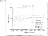
- Optical transmittance of the conductive film was obtained by a hybrid method (HSE06 method) and a result thereof is illustrated in FIG 7 . Electrical conductivity is illustrated in FIG 8 .
- transmittance of visible light was as high as 87 to 91%. Further, at room temperature (300K), electrical conductivity of the conductive film containing InAlO 3 (ZnO) 4 was about 10 -3 S/cm and electrical conductivity of the conductive film containing InGaO 3 (ZnO) 4 was about 10 -4 S/cm.
Landscapes
- Chemical & Material Sciences (AREA)
- Organic Chemistry (AREA)
- Inorganic Chemistry (AREA)
- Physics & Mathematics (AREA)
- Electromagnetism (AREA)
- Engineering & Computer Science (AREA)
- Manufacturing & Machinery (AREA)
- Non-Insulated Conductors (AREA)
- Thin Film Transistor (AREA)
- Physical Vapour Deposition (AREA)
- Composite Materials (AREA)
- Materials Engineering (AREA)
- Electrodes Of Semiconductors (AREA)
- Manufacturing Of Electric Cables (AREA)
- Photovoltaic Devices (AREA)
Claims (10)
- Transparente leitfähige Folie, umfassend eine Verbindung mit einer kristallinen Struktur und dargestellt durch chemische Formel 1,
wobei die durch chemische Formel 1 dagestellte Verbindung zusätzlich mit einem n-artigen Dotanden dotiert ist, und
wobei der n-artige Dotand wenigstens eines ausgewählt aus der Gruppe bestehend aus Sn, Ge und Mo umfasst:
[Chemische Formel] [(RpXq)O3]m(AO)n
wobeiR Sc, Fe, Cu, Ga, Y, In, Er, Tm, Yb oder Lu ist,X Al ist,ein Gehalt des X 50% oder weniger eines Gehalts des R ist, undA Mg, Mn, Co oder Zn ist,m 1 bis 4 ist,n 1 bis 7 ist, undp und q ein Atomgehaltsverhältnis von größer als 0 bis 1 oder weniger unabhängig voneinander darstellen. - Transparente leitfähige Folie nach Anspruch 1, wobei das R der chemischen Formel 1 In oder Lu ist.
- Transparente leitfähige Folie nach Anspruch 1, wobei die durch chemische Formel 1 dargestellte Verbindung InAlO3(ZnO), ist, und wobei das n 1 bis 7 ist.
- Verfahren zum Herstellen einer transparenten leitfähigen Folie umfassend Bilden, auf einem Substrat, einer Verbindung mit einer kristallinen Struktur und dargestellt durch chemische Formel 1,
wobei das Bilden einer durch chemische Formel 1 dargestellten Verbindung ein DC/RF-Magnetronsputterverfahren oder ein Molekularstrahlepitaxieverfahren verwendet,
wobei die durch chemische Formel 1 dargestellte Verbindung zusätzlich mit einem n-artigen Dotanden dotiert ist, und
wobei der n-artige Dotand wenigstens eines ausgewählt aus der Gruppe bestehend aus Sn, Ge und Mo umfasst:
[Chemische Formel 1] [(RpXq)O3]m(AO)n
wobeiR Sc, Fe, Cu, Ga, Y, In, Er, Tm, Yb oder Lu ist,X Al ist,ein Gehalt des X 50% oder weniger eines Gehalts des R ist, undA Mg, Mn, Co oder Zn ist,m 1 bis 4 ist,n 1 bis 7 ist, undp und q ein Atomgehaltsverhältnis von größer als 0 bis 1 oder weniger unabhängig voneinander darstellen. - Verfahren zum Herstellen einer transparenten leitfähigen Folie nach Anspruch 4, wobei die durch chemische Formel 1 dargestellte Verbindung InAlO3(ZnO)n ist, und wobei das n 1 bis 7 ist.
- Elektronisches Bauelement umfassend die transparente leitfähige Folie nach einem der Ansprüche 1 bis 3.
- Dünnschichttransistor umfassend die transparente leitfähige Folie nach einem der Ansprüche 1 bis 3.
- Dünnschichttransistor nach Anspruch 7, wobei der Dünnschichttransistor eine Gate-Elektrode, eine Gate-Isolierschicht, eine aktive Schicht, eine Source-Elektrode und eine Drain-Elektrode auf einem Substrat umfasst, und
wobei die Gate-Elektrode, die Gate-Isolierschicht, die aktive Schicht, die Source-Elektrode und die Drain-Elektrode die durch chemische Formel 1 dargestellte Verbindung umfassen. - Dünnschichttransistor nach Anspruch 8, wobei die Gate-Elektrode InAlSnO3(ZnO)4 umfasst.
- Dünnschichttransistor nach Anspruch 8, wobei die Source-Elektrode und die Drain-Elektrode InAlSnO3(ZnO)4 umfassen.
Applications Claiming Priority (2)
| Application Number | Priority Date | Filing Date | Title |
|---|---|---|---|
| KR20120103498 | 2012-09-18 | ||
| PCT/KR2013/008444 WO2014046480A1 (ko) | 2012-09-18 | 2013-09-17 | 투명 전도성막 및 이의 제조방법 |
Publications (3)
| Publication Number | Publication Date |
|---|---|
| EP2866232A1 EP2866232A1 (de) | 2015-04-29 |
| EP2866232A4 EP2866232A4 (de) | 2016-04-06 |
| EP2866232B1 true EP2866232B1 (de) | 2018-03-07 |
Family
ID=50341701
Family Applications (1)
| Application Number | Title | Priority Date | Filing Date |
|---|---|---|---|
| EP13839469.7A Active EP2866232B1 (de) | 2012-09-18 | 2013-09-17 | Transparente leitfähige folie und herstellungsverfahren dafür |
Country Status (7)
| Country | Link |
|---|---|
| US (1) | US9577109B2 (de) |
| EP (1) | EP2866232B1 (de) |
| JP (1) | JP6080141B2 (de) |
| KR (1) | KR101472219B1 (de) |
| CN (1) | CN104584139B (de) |
| TW (1) | TWI543195B (de) |
| WO (1) | WO2014046480A1 (de) |
Families Citing this family (8)
| Publication number | Priority date | Publication date | Assignee | Title |
|---|---|---|---|---|
| CN104167448B (zh) * | 2014-08-05 | 2017-06-30 | 京东方科技集团股份有限公司 | 薄膜晶体管及其制备方法、阵列基板和显示装置 |
| DE102015213305A1 (de) | 2015-07-15 | 2017-01-19 | Saint-Augustin Canada Electric Inc. | Optisches Lichttransmissionselement für eine Solarenergieanordnung mit einem Erntebereich und einem Justiersteuerungsbereich, und Verfahren zur Justierung desselben |
| CN106711195B (zh) * | 2016-10-20 | 2020-01-17 | 浙江大学 | 一种p型ZnMSnO非晶氧化物半导体薄膜及其制备方法 |
| CN106711228B (zh) * | 2016-10-20 | 2020-03-03 | 浙江大学 | 一种p型LaMSnO非晶氧化物半导体薄膜及其制备方法 |
| CN106711201B (zh) * | 2016-10-20 | 2020-01-17 | 浙江大学 | 一种p型CrMCuO非晶氧化物半导体薄膜及其制备方法 |
| CN106711202A (zh) * | 2016-10-20 | 2017-05-24 | 浙江大学 | 一种p型ZnAlSnO非晶氧化物半导体薄膜及其制备方法 |
| US11056593B2 (en) | 2017-09-12 | 2021-07-06 | Intel Corporation | Semiconductor devices with metal contacts including crystalline alloys |
| CN113135600B (zh) * | 2021-03-03 | 2022-05-13 | 重庆文理学院 | 一种非晶态氧化铁薄膜的制备方法 |
Family Cites Families (17)
| Publication number | Priority date | Publication date | Assignee | Title |
|---|---|---|---|---|
| JP3945887B2 (ja) * | 1998-01-30 | 2007-07-18 | Hoya株式会社 | 導電性酸化物薄膜を有する物品及びその製造方法 |
| JP3423896B2 (ja) * | 1999-03-25 | 2003-07-07 | 科学技術振興事業団 | 半導体デバイス |
| JP3531865B2 (ja) * | 2000-07-06 | 2004-05-31 | 独立行政法人 科学技術振興機構 | 超平坦透明導電膜およびその製造方法 |
| EP1443130B1 (de) | 2001-11-05 | 2011-09-28 | Japan Science and Technology Agency | Homologer einkristalliner dünner film mit natürlichem supergitter, herstellungsverfahren dafür und vorrichtung, bei der der einkristalline dünne film verwendet wird |
| JP3803592B2 (ja) * | 2002-02-26 | 2006-08-02 | 株式会社アルバック | 低抵抗透明導電膜及びその製造法 |
| EP1737044B1 (de) | 2004-03-12 | 2014-12-10 | Japan Science and Technology Agency | Amorphes oxid und dünnfilmtransistor |
| KR100998527B1 (ko) | 2004-11-10 | 2010-12-07 | 고쿠리츠다이가쿠호진 토쿄고교 다이가꾸 | 비정질 산화물 및 전계 효과 트랜지스터 |
| JP4836229B2 (ja) * | 2005-05-31 | 2011-12-14 | 株式会社東芝 | 蛍光体および発光装置 |
| JP5058469B2 (ja) * | 2005-09-06 | 2012-10-24 | キヤノン株式会社 | スパッタリングターゲットおよび該ターゲットを用いた薄膜の形成方法 |
| JP2009123957A (ja) * | 2007-11-15 | 2009-06-04 | Sumitomo Chemical Co Ltd | 酸化物半導体材料及びその製造方法、電子デバイス及び電界効果トランジスタ |
| US8455371B2 (en) * | 2008-05-22 | 2013-06-04 | Idemitsu Kosan Co., Ltd. | Sputtering target, method for forming amorphous oxide thin film using the same, and method for manufacturing thin film transistor |
| CN103204674A (zh) * | 2008-12-15 | 2013-07-17 | 出光兴产株式会社 | 氧化铟系烧结体及溅射靶 |
| JP5468801B2 (ja) * | 2009-03-23 | 2014-04-09 | 株式会社カネカ | 透明電極付き基板およびその製造方法 |
| EP2449593B1 (de) * | 2009-07-03 | 2019-08-28 | Semiconductor Energy Laboratory Co, Ltd. | Herstellungsverfahren für halbleiterbauelement |
| KR20110022813A (ko) * | 2009-08-28 | 2011-03-08 | 삼성코닝정밀소재 주식회사 | 산화아연계 전도체 및 그 제조방법 |
| WO2011024296A1 (ja) * | 2009-08-28 | 2011-03-03 | 株式会社 東芝 | 蛍光体の製造方法およびそれにより製造された蛍光体 |
| JP5708910B2 (ja) | 2010-03-30 | 2015-04-30 | ソニー株式会社 | 薄膜トランジスタおよびその製造方法、並びに表示装置 |
-
2013
- 2013-09-17 JP JP2015529700A patent/JP6080141B2/ja active Active
- 2013-09-17 KR KR1020130112118A patent/KR101472219B1/ko active Active
- 2013-09-17 CN CN201380044464.6A patent/CN104584139B/zh active Active
- 2013-09-17 US US14/419,847 patent/US9577109B2/en active Active
- 2013-09-17 EP EP13839469.7A patent/EP2866232B1/de active Active
- 2013-09-17 WO PCT/KR2013/008444 patent/WO2014046480A1/ko not_active Ceased
- 2013-09-18 TW TW102133810A patent/TWI543195B/zh active
Non-Patent Citations (1)
| Title |
|---|
| None * |
Also Published As
| Publication number | Publication date |
|---|---|
| TWI543195B (zh) | 2016-07-21 |
| CN104584139B (zh) | 2017-03-01 |
| EP2866232A1 (de) | 2015-04-29 |
| EP2866232A4 (de) | 2016-04-06 |
| JP2015535881A (ja) | 2015-12-17 |
| TW201426763A (zh) | 2014-07-01 |
| KR101472219B1 (ko) | 2014-12-11 |
| CN104584139A (zh) | 2015-04-29 |
| KR20140036991A (ko) | 2014-03-26 |
| WO2014046480A1 (ko) | 2014-03-27 |
| US9577109B2 (en) | 2017-02-21 |
| JP6080141B2 (ja) | 2017-02-15 |
| US20150194531A1 (en) | 2015-07-09 |
Similar Documents
| Publication | Publication Date | Title |
|---|---|---|
| EP2866232B1 (de) | Transparente leitfähige folie und herstellungsverfahren dafür | |
| EP2537185B1 (de) | Feldeffekttransistor, anzeigeelement, bildanzeigevorrichtung und system dafür | |
| Wang et al. | Effect of substrate temperature on transparent conducting Al and F co-doped ZnO thin films prepared by rf magnetron sputtering | |
| Fortunato et al. | Highly stable transparent and conducting gallium-doped zinc oxide thin films for photovoltaic applications | |
| US10366803B2 (en) | Metal oxide thin film, method for depositing metal oxide thin film and device comprising metal oxide thin film | |
| US20110141076A1 (en) | Semiconductor device, method for manufacturing semiconductor device, transistor substrate, light emitting device and display device | |
| Jayathilake et al. | Overview on transparent conducting oxides and state of the art of low-cost doped ZnO systems | |
| Wei et al. | Growth, Microstructures, and Optoelectronic Properties of Epitaxial BaSn1–x Sb x O3− δ Thin Films by Chemical Solution Deposition | |
| US8253012B2 (en) | High quality transparent conducting oxide thin films | |
| Elangovan et al. | RF sputtered wide work function indium molybdenum oxide thin films for solar cell applications | |
| KR101183967B1 (ko) | 경사기능 투명전도성 산화막 및 그 제조방법, 경사기능 투명전도성 산화막을 이용한 유기발광다이오드용 양극 및 태양전지용 윈도우층 | |
| US11624109B2 (en) | Method for manufacturing transparent conductive film | |
| US9546415B2 (en) | Composite transparent electrodes | |
| Lu et al. | Fabrication of low-resistive p-type Al–N co-doped zinc oxide thin films by RF reactive magnetron sputtering | |
| US9666324B2 (en) | Transparent conductive thin film | |
| KR100733915B1 (ko) | 고분자 재료 기판에 완충층이 증착된 투명 전도성 산화막및 그 제조방법 | |
| Chu et al. | Effect of annealing conditions on the structural, electrical and optical properties of Li-doped NiO thin films | |
| KR101807957B1 (ko) | 산화물 기반 고 전도성 유연 투명전극 및 이의 제조방법 | |
| KR20070021342A (ko) | 마그네트론 스퍼터링법을 이용한 산소/아르곤 유량비 조절을 통한 금속이 도핑된 ZnO 박막의 제조방법 | |
| Chen et al. | Improvement of Electrical and Wet-Etching Characteristics for Ingatio Electrodes in Organic Light-Emitting Diodes Through Hydrogen Doping | |
| KR20080016034A (ko) | 마그네트론 스퍼터링법을 이용한 gzo 박막의 제조방법 |
Legal Events
| Date | Code | Title | Description |
|---|---|---|---|
| PUAI | Public reference made under article 153(3) epc to a published international application that has entered the european phase |
Free format text: ORIGINAL CODE: 0009012 |
|
| 17P | Request for examination filed |
Effective date: 20150123 |
|
| AK | Designated contracting states |
Kind code of ref document: A1 Designated state(s): AL AT BE BG CH CY CZ DE DK EE ES FI FR GB GR HR HU IE IS IT LI LT LU LV MC MK MT NL NO PL PT RO RS SE SI SK SM TR |
|
| AX | Request for extension of the european patent |
Extension state: BA ME |
|
| DAX | Request for extension of the european patent (deleted) | ||
| RA4 | Supplementary search report drawn up and despatched (corrected) |
Effective date: 20160303 |
|
| RIC1 | Information provided on ipc code assigned before grant |
Ipc: H01L 29/51 20060101ALI20160226BHEP Ipc: H01L 51/52 20060101ALI20160226BHEP Ipc: H01L 29/49 20060101ALI20160226BHEP Ipc: C01G 15/00 20060101ALI20160226BHEP Ipc: H01L 29/45 20060101ALI20160226BHEP Ipc: H01L 29/786 20060101ALI20160226BHEP Ipc: H01B 5/14 20060101ALI20160226BHEP Ipc: H01B 1/08 20060101AFI20160226BHEP Ipc: H01L 31/0224 20060101ALI20160226BHEP Ipc: H01L 51/44 20060101ALI20160226BHEP Ipc: H01B 13/00 20060101ALI20160226BHEP |
|
| 17Q | First examination report despatched |
Effective date: 20170210 |
|
| GRAP | Despatch of communication of intention to grant a patent |
Free format text: ORIGINAL CODE: EPIDOSNIGR1 |
|
| INTG | Intention to grant announced |
Effective date: 20180103 |
|
| RAX | Requested extension states of the european patent have changed |
Extension state: BA Extension state: ME |
|
| GRAS | Grant fee paid |
Free format text: ORIGINAL CODE: EPIDOSNIGR3 |
|
| GRAA | (expected) grant |
Free format text: ORIGINAL CODE: 0009210 |
|
| AK | Designated contracting states |
Kind code of ref document: B1 Designated state(s): AL AT BE BG CH CY CZ DE DK EE ES FI FR GB GR HR HU IE IS IT LI LT LU LV MC MK MT NL NO PL PT RO RS SE SI SK SM TR |
|
| DAX | Request for extension of the european patent (deleted) | ||
| REG | Reference to a national code |
Ref country code: GB Ref legal event code: FG4D |
|
| REG | Reference to a national code |
Ref country code: CH Ref legal event code: EP Ref country code: AT Ref legal event code: REF Ref document number: 977382 Country of ref document: AT Kind code of ref document: T Effective date: 20180315 |
|
| REG | Reference to a national code |
Ref country code: IE Ref legal event code: FG4D |
|
| REG | Reference to a national code |
Ref country code: DE Ref legal event code: R096 Ref document number: 602013034211 Country of ref document: DE |
|
| REG | Reference to a national code |
Ref country code: NL Ref legal event code: MP Effective date: 20180307 |
|
| REG | Reference to a national code |
Ref country code: LT Ref legal event code: MG4D |
|
| PG25 | Lapsed in a contracting state [announced via postgrant information from national office to epo] |
Ref country code: FI Free format text: LAPSE BECAUSE OF FAILURE TO SUBMIT A TRANSLATION OF THE DESCRIPTION OR TO PAY THE FEE WITHIN THE PRESCRIBED TIME-LIMIT Effective date: 20180307 Ref country code: LT Free format text: LAPSE BECAUSE OF FAILURE TO SUBMIT A TRANSLATION OF THE DESCRIPTION OR TO PAY THE FEE WITHIN THE PRESCRIBED TIME-LIMIT Effective date: 20180307 Ref country code: CY Free format text: LAPSE BECAUSE OF FAILURE TO SUBMIT A TRANSLATION OF THE DESCRIPTION OR TO PAY THE FEE WITHIN THE PRESCRIBED TIME-LIMIT Effective date: 20180307 Ref country code: HR Free format text: LAPSE BECAUSE OF FAILURE TO SUBMIT A TRANSLATION OF THE DESCRIPTION OR TO PAY THE FEE WITHIN THE PRESCRIBED TIME-LIMIT Effective date: 20180307 Ref country code: NO Free format text: LAPSE BECAUSE OF FAILURE TO SUBMIT A TRANSLATION OF THE DESCRIPTION OR TO PAY THE FEE WITHIN THE PRESCRIBED TIME-LIMIT Effective date: 20180607 Ref country code: ES Free format text: LAPSE BECAUSE OF FAILURE TO SUBMIT A TRANSLATION OF THE DESCRIPTION OR TO PAY THE FEE WITHIN THE PRESCRIBED TIME-LIMIT Effective date: 20180307 |
|
| REG | Reference to a national code |
Ref country code: AT Ref legal event code: MK05 Ref document number: 977382 Country of ref document: AT Kind code of ref document: T Effective date: 20180307 |
|
| REG | Reference to a national code |
Ref country code: FR Ref legal event code: PLFP Year of fee payment: 6 |
|
| PG25 | Lapsed in a contracting state [announced via postgrant information from national office to epo] |
Ref country code: RS Free format text: LAPSE BECAUSE OF FAILURE TO SUBMIT A TRANSLATION OF THE DESCRIPTION OR TO PAY THE FEE WITHIN THE PRESCRIBED TIME-LIMIT Effective date: 20180307 Ref country code: BG Free format text: LAPSE BECAUSE OF FAILURE TO SUBMIT A TRANSLATION OF THE DESCRIPTION OR TO PAY THE FEE WITHIN THE PRESCRIBED TIME-LIMIT Effective date: 20180607 Ref country code: SE Free format text: LAPSE BECAUSE OF FAILURE TO SUBMIT A TRANSLATION OF THE DESCRIPTION OR TO PAY THE FEE WITHIN THE PRESCRIBED TIME-LIMIT Effective date: 20180307 Ref country code: LV Free format text: LAPSE BECAUSE OF FAILURE TO SUBMIT A TRANSLATION OF THE DESCRIPTION OR TO PAY THE FEE WITHIN THE PRESCRIBED TIME-LIMIT Effective date: 20180307 Ref country code: GR Free format text: LAPSE BECAUSE OF FAILURE TO SUBMIT A TRANSLATION OF THE DESCRIPTION OR TO PAY THE FEE WITHIN THE PRESCRIBED TIME-LIMIT Effective date: 20180608 |
|
| PG25 | Lapsed in a contracting state [announced via postgrant information from national office to epo] |
Ref country code: IT Free format text: LAPSE BECAUSE OF FAILURE TO SUBMIT A TRANSLATION OF THE DESCRIPTION OR TO PAY THE FEE WITHIN THE PRESCRIBED TIME-LIMIT Effective date: 20180307 Ref country code: NL Free format text: LAPSE BECAUSE OF FAILURE TO SUBMIT A TRANSLATION OF THE DESCRIPTION OR TO PAY THE FEE WITHIN THE PRESCRIBED TIME-LIMIT Effective date: 20180307 Ref country code: EE Free format text: LAPSE BECAUSE OF FAILURE TO SUBMIT A TRANSLATION OF THE DESCRIPTION OR TO PAY THE FEE WITHIN THE PRESCRIBED TIME-LIMIT Effective date: 20180307 Ref country code: RO Free format text: LAPSE BECAUSE OF FAILURE TO SUBMIT A TRANSLATION OF THE DESCRIPTION OR TO PAY THE FEE WITHIN THE PRESCRIBED TIME-LIMIT Effective date: 20180307 Ref country code: AL Free format text: LAPSE BECAUSE OF FAILURE TO SUBMIT A TRANSLATION OF THE DESCRIPTION OR TO PAY THE FEE WITHIN THE PRESCRIBED TIME-LIMIT Effective date: 20180307 Ref country code: PL Free format text: LAPSE BECAUSE OF FAILURE TO SUBMIT A TRANSLATION OF THE DESCRIPTION OR TO PAY THE FEE WITHIN THE PRESCRIBED TIME-LIMIT Effective date: 20180307 |
|
| PG25 | Lapsed in a contracting state [announced via postgrant information from national office to epo] |
Ref country code: AT Free format text: LAPSE BECAUSE OF FAILURE TO SUBMIT A TRANSLATION OF THE DESCRIPTION OR TO PAY THE FEE WITHIN THE PRESCRIBED TIME-LIMIT Effective date: 20180307 Ref country code: SK Free format text: LAPSE BECAUSE OF FAILURE TO SUBMIT A TRANSLATION OF THE DESCRIPTION OR TO PAY THE FEE WITHIN THE PRESCRIBED TIME-LIMIT Effective date: 20180307 Ref country code: SM Free format text: LAPSE BECAUSE OF FAILURE TO SUBMIT A TRANSLATION OF THE DESCRIPTION OR TO PAY THE FEE WITHIN THE PRESCRIBED TIME-LIMIT Effective date: 20180307 Ref country code: CZ Free format text: LAPSE BECAUSE OF FAILURE TO SUBMIT A TRANSLATION OF THE DESCRIPTION OR TO PAY THE FEE WITHIN THE PRESCRIBED TIME-LIMIT Effective date: 20180307 |
|
| REG | Reference to a national code |
Ref country code: DE Ref legal event code: R097 Ref document number: 602013034211 Country of ref document: DE |
|
| PG25 | Lapsed in a contracting state [announced via postgrant information from national office to epo] |
Ref country code: PT Free format text: LAPSE BECAUSE OF FAILURE TO SUBMIT A TRANSLATION OF THE DESCRIPTION OR TO PAY THE FEE WITHIN THE PRESCRIBED TIME-LIMIT Effective date: 20180709 |
|
| PLBE | No opposition filed within time limit |
Free format text: ORIGINAL CODE: 0009261 |
|
| STAA | Information on the status of an ep patent application or granted ep patent |
Free format text: STATUS: NO OPPOSITION FILED WITHIN TIME LIMIT |
|
| PG25 | Lapsed in a contracting state [announced via postgrant information from national office to epo] |
Ref country code: DK Free format text: LAPSE BECAUSE OF FAILURE TO SUBMIT A TRANSLATION OF THE DESCRIPTION OR TO PAY THE FEE WITHIN THE PRESCRIBED TIME-LIMIT Effective date: 20180307 |
|
| 26N | No opposition filed |
Effective date: 20181210 |
|
| PG25 | Lapsed in a contracting state [announced via postgrant information from national office to epo] |
Ref country code: SI Free format text: LAPSE BECAUSE OF FAILURE TO SUBMIT A TRANSLATION OF THE DESCRIPTION OR TO PAY THE FEE WITHIN THE PRESCRIBED TIME-LIMIT Effective date: 20180307 |
|
| PG25 | Lapsed in a contracting state [announced via postgrant information from national office to epo] |
Ref country code: MC Free format text: LAPSE BECAUSE OF FAILURE TO SUBMIT A TRANSLATION OF THE DESCRIPTION OR TO PAY THE FEE WITHIN THE PRESCRIBED TIME-LIMIT Effective date: 20180307 |
|
| REG | Reference to a national code |
Ref country code: CH Ref legal event code: PL |
|
| REG | Reference to a national code |
Ref country code: BE Ref legal event code: MM Effective date: 20180930 |
|
| REG | Reference to a national code |
Ref country code: IE Ref legal event code: MM4A |
|
| PG25 | Lapsed in a contracting state [announced via postgrant information from national office to epo] |
Ref country code: LU Free format text: LAPSE BECAUSE OF NON-PAYMENT OF DUE FEES Effective date: 20180917 |
|
| PG25 | Lapsed in a contracting state [announced via postgrant information from national office to epo] |
Ref country code: IE Free format text: LAPSE BECAUSE OF NON-PAYMENT OF DUE FEES Effective date: 20180917 |
|
| PG25 | Lapsed in a contracting state [announced via postgrant information from national office to epo] |
Ref country code: BE Free format text: LAPSE BECAUSE OF NON-PAYMENT OF DUE FEES Effective date: 20180930 Ref country code: CH Free format text: LAPSE BECAUSE OF NON-PAYMENT OF DUE FEES Effective date: 20180930 Ref country code: LI Free format text: LAPSE BECAUSE OF NON-PAYMENT OF DUE FEES Effective date: 20180930 |
|
| PG25 | Lapsed in a contracting state [announced via postgrant information from national office to epo] |
Ref country code: MT Free format text: LAPSE BECAUSE OF NON-PAYMENT OF DUE FEES Effective date: 20180917 |
|
| PG25 | Lapsed in a contracting state [announced via postgrant information from national office to epo] |
Ref country code: TR Free format text: LAPSE BECAUSE OF FAILURE TO SUBMIT A TRANSLATION OF THE DESCRIPTION OR TO PAY THE FEE WITHIN THE PRESCRIBED TIME-LIMIT Effective date: 20180307 |
|
| PG25 | Lapsed in a contracting state [announced via postgrant information from national office to epo] |
Ref country code: HU Free format text: LAPSE BECAUSE OF FAILURE TO SUBMIT A TRANSLATION OF THE DESCRIPTION OR TO PAY THE FEE WITHIN THE PRESCRIBED TIME-LIMIT; INVALID AB INITIO Effective date: 20130917 |
|
| PG25 | Lapsed in a contracting state [announced via postgrant information from national office to epo] |
Ref country code: MK Free format text: LAPSE BECAUSE OF NON-PAYMENT OF DUE FEES Effective date: 20180307 |
|
| PG25 | Lapsed in a contracting state [announced via postgrant information from national office to epo] |
Ref country code: IS Free format text: LAPSE BECAUSE OF FAILURE TO SUBMIT A TRANSLATION OF THE DESCRIPTION OR TO PAY THE FEE WITHIN THE PRESCRIBED TIME-LIMIT Effective date: 20180707 |
|
| PGFP | Annual fee paid to national office [announced via postgrant information from national office to epo] |
Ref country code: DE Payment date: 20250820 Year of fee payment: 13 |
|
| PGFP | Annual fee paid to national office [announced via postgrant information from national office to epo] |
Ref country code: GB Payment date: 20250820 Year of fee payment: 13 |
|
| PGFP | Annual fee paid to national office [announced via postgrant information from national office to epo] |
Ref country code: FR Payment date: 20250821 Year of fee payment: 13 |