EP2866347B1 - Commutateur auto-élévateur isolé - Google Patents
Commutateur auto-élévateur isolé Download PDFInfo
- Publication number
- EP2866347B1 EP2866347B1 EP14002509.9A EP14002509A EP2866347B1 EP 2866347 B1 EP2866347 B1 EP 2866347B1 EP 14002509 A EP14002509 A EP 14002509A EP 2866347 B1 EP2866347 B1 EP 2866347B1
- Authority
- EP
- European Patent Office
- Prior art keywords
- terminal
- switch
- circuit
- input
- capacitor
- Prior art date
- Legal status (The legal status is an assumption and is not a legal conclusion. Google has not performed a legal analysis and makes no representation as to the accuracy of the status listed.)
- Active
Links
Images




Classifications
-
- H—ELECTRICITY
- H03—ELECTRONIC CIRCUITRY
- H03K—PULSE TECHNIQUE
- H03K17/00—Electronic switching or gating, i.e. not by contact-making and –breaking
- H03K17/06—Modifications for ensuring a fully conducting state
- H03K17/063—Modifications for ensuring a fully conducting state in field-effect transistor switches
-
- G—PHYSICS
- G11—INFORMATION STORAGE
- G11C—STATIC STORES
- G11C27/00—Electric analogue stores, e.g. for storing instantaneous values
- G11C27/02—Sample-and-hold arrangements
-
- H—ELECTRICITY
- H03—ELECTRONIC CIRCUITRY
- H03K—PULSE TECHNIQUE
- H03K17/00—Electronic switching or gating, i.e. not by contact-making and –breaking
- H03K17/16—Modifications for eliminating interference voltages or currents
- H03K17/161—Modifications for eliminating interference voltages or currents in field-effect transistor switches
- H03K17/165—Modifications for eliminating interference voltages or currents in field-effect transistor switches by feedback from the output circuit to the control circuit
-
- H—ELECTRICITY
- H03—ELECTRONIC CIRCUITRY
- H03K—PULSE TECHNIQUE
- H03K3/00—Circuits for generating electric pulses; Monostable, bistable or multistable circuits
- H03K3/02—Generators characterised by the type of circuit or by the means used for producing pulses
- H03K3/353—Generators characterised by the type of circuit or by the means used for producing pulses by the use, as active elements, of field-effect transistors with internal or external positive feedback
- H03K3/356—Bistable circuits
- H03K3/356017—Bistable circuits using additional transistors in the input circuit
- H03K3/356034—Bistable circuits using additional transistors in the input circuit the input circuit having a differential configuration
-
- H—ELECTRICITY
- H03—ELECTRONIC CIRCUITRY
- H03M—CODING; DECODING; CODE CONVERSION IN GENERAL
- H03M1/00—Analogue/digital conversion; Digital/analogue conversion
- H03M1/12—Analogue/digital converters
- H03M1/124—Sampling or signal conditioning arrangements specially adapted for A/D converters
-
- H—ELECTRICITY
- H03—ELECTRONIC CIRCUITRY
- H03M—CODING; DECODING; CODE CONVERSION IN GENERAL
- H03M1/00—Analogue/digital conversion; Digital/analogue conversion
- H03M1/12—Analogue/digital converters
- H03M1/124—Sampling or signal conditioning arrangements specially adapted for A/D converters
- H03M1/129—Means for adapting the input signal to the range the converter can handle, e.g. limiting, pre-scaling ; Out-of-range indication
-
- H—ELECTRICITY
- H03—ELECTRONIC CIRCUITRY
- H03K—PULSE TECHNIQUE
- H03K2217/00—Indexing scheme related to electronic switching or gating, i.e. not by contact-making or -breaking covered by H03K17/00
- H03K2217/0009—AC switches, i.e. delivering AC power to a load
-
- H—ELECTRICITY
- H03—ELECTRONIC CIRCUITRY
- H03K—PULSE TECHNIQUE
- H03K2217/00—Indexing scheme related to electronic switching or gating, i.e. not by contact-making or -breaking covered by H03K17/00
- H03K2217/0054—Gating switches, e.g. pass gates
Definitions
- the present invention relates to an input circuit for sampling an analog signal.
- the present invention relates to an input circuit for sampling an analog differential signal with a wide common mode range.
- ADC analog-to-digital converter
- Figure 1 shows a switching circuit that is disclosed in U.S. Patent 8,022,679 (“the '679 patent”), entitled “SYSTEMS AND METHODS FOR FAST SWITCH TURN ON APPROXIMATING IDEAL DIODE FUNCTION.”
- the switching circuit of the '679 patent is not fully capacitively isolated, and its charge pump is not referenced to a source terminal of the switch.
- the switching circuit has neither a discriminator nor a voltage regulator to provide a well-controlled gate-to- source voltage (V GS ). Therefore, the switching circuit of the '679 patent cannot operate below the ground reference and thus is not suitable for use in a sampling network for an ADC.
- FIG. 2 shows a bootstrapped switch circuit disclosed in US Patent Application US 2006/0202735 and in U.S. Patent 7,176,742 (“the '742 patent"), entitled “BOOTSTRAPPED SWITCH WITH AN INPUT DYNAMIC RANGE GREATER THAN SUPPLY VOLTAGE.”
- the bootstrapped switch circuit of the '742 patent may be used for sampling an input signal that goes beyond the power supply voltages.
- this bootstrapped switch circuit is capable of accepting an input signal that exceeds the supply voltage on the positive side by a limited amount, as the several low voltage transistors in the bootstrapping circuit is unable to withstand higher voltage signals.
- the bootstrapped switch circuit of the '742 patent includes capacitor C13 that is precharged by being first connected between supply voltages GND and VDD. The charged capacitor is then switched to being connected between the source and gate terminals of bootstrapped switch MN20. For high input signals, precharged capacitor C13 must swing up to the input signal. The parasitic capacitors in bootstrapped switch MMN20 result in a signal-dependent V GS .
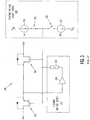
- FIG. 3 shows a bipolar switch that is disclosed in U.S. Patent Application Publication 2013/009623 (“the '623 publication”), entitled “FOUR-QUADRANT BOOTSTRAPPED SWITCH CIRCUIT.”
- the bipolar switch in the '623 publication is operated by a floating voltage source.
- the switch of the '623 publication cannot accept an input signal that can go beyond the supply voltages, as the floating voltage source is generated by current sources that operate between those supply voltages.
- U.S. Patent Application 2007/139092 A1 discloses a low to high voltage level converter which includes first and second n-channel transistors arranged to force to the ground voltage a first connection node and a second connection node, respectively.
- a boosting circuit operates to boost an input voltage of at least one of a first and second control nodes for the first and second n-channel transistors above a low voltage level.
- the converter further includes first and second cross-coupled p-channel transistors arranged to force to the high voltage level the first connection node and the second connection node, respectively.
- a digital output signal is taken from one of the first and second connection nodes.
- U.S. Patent Application 5 831 562 A discloses a full differential sample and hold circuit for an analog to digital converter.
- the sample and hold circuit samples and holds the differential signal resulting from two input signals.
- the sample and hold circuit includes a comparator, two differential capacitors and a common mode sample and hold circuit.
- the comparator has two input terminals and an output terminal.
- Each of the differential capacitors corresponds to one of the input signals and has an input terminal adapted for selective coupling to the respective input signal.
- Each of the differential capacitors has an output terminal electrically coupled to a different input terminal of the comparator.
- the common mode sample and hold circuit is disposed between the input terminals of the two differential capacitors.
- the common mode sample and hold circuit comprises two common mode capacitors.
- Each of the common mode capacitors has an output terminal electrically coupled to a reference voltage and an input terminal electrically coupled to the input terminal of a different differential capacitor.
- the reference voltage is ground.
- the invention also relates to a method of sampling and holding a differential signal.
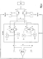
- FIG. 4 shows a sampling network with switching circuits that is described in the present inventor's copending U.S. Patent Application (“Copending Patent Application”), entitled “BIPOLAR ISOLATED HIGH VOLTAGE SAMPLING NETWORK.”
- the sampling network uses ground-referenced charge pumps, and thus the switches in the sampling network are unable to establish a constant V GS for a rapidly changing input signal.
- PMOS transistors with their N-Wells connected to the input signal render the switches unable to operate below substrate potential because the open circuit in the diode to the p-substrate.
- the signal polarity comparator in Figure 4 is required to operate beyond the supply voltages.
- FIG. 5(a) is block diagram 100 of a bootstrapped switch circuit, showing source terminal OUT of bootstrapped switch S1 being connected to charge pump CP, in accordance with one embodiment of the present invention.
- charge pump CP generates a voltage difference to supply the operation of CMOS logic circuit 101.
- CMOS logic circuit 101 controls the gate-to-source voltage (V GS ) of bootstrapped switch S1, which switches bootstrapped switch S1 between conducting and non-conducting states.
- V GS gate-to-source voltage
- Bootstrapped switch S1 when in the conducting state, passes the input signal at drain terminal IN to source terminal OUT.
- Charge pump CP and CMOS logic circuit 101 are controlled by clock signals PHI1, PHI2, PHIC1 and PHIC2, respectively, which are provided by timing control unit 102 via capacitors. Other than these capacitor-coupled clock signals, bootstrapped switch S1, charge pump CP and CMOS logic circuit 101 are isolated from power supply voltages VDD and GND. Timing control unit 102 draws power from power supply voltages VDD and GND.
- FIG. 5(b) shows the waveforms of clock signals PHI1, PHI2, PHIC1 and PHIC2, according to one embodiment of the present invention.
- clock signals PHI1 and PHI2 are substantially complementary and non-overlapping (i.e., having a time delay between the rising or falling edge of each clock signal and the immediately following rising or falling edge of the other signal).
- Clock signals PHIC1 and PHIC2 are similarly complementary and non-overlapping.
- FIG. 6 is a schematic diagram showing bootstrapped switch circuit 200, which is an implementation of charge pump CP, CMOS logic circuit 101 and bootstrapped switch S1 of Figure 5(a) , in accordance with one embodiment of the present invention.
- charge pump CP includes NMOS transistors T2, T3, T4, and T5 and capacitors C1, C2 and C3.
- Clock signals PHI1D and PHI2D have substantially the same waveforms as clock signals PHI1 and PHI2 of Figure 5(b) , which alternately charge capacitors C1 and C2.
- bootstrapped switch S1 is implemented by NMOS transistor T1.
- CMOS logic circuit 101 is implemented by PMOS transistorsT7 and T9, NMOS transistors T6 and T8, capacitors C4 and C5, and resistors that are connected cross each of the gate terminals of NMOS transistors T6 and T8 and source terminal IN of bootstrapped switch S1.
- CMOS logic circuit 101 is implemented as a latch structure with a stored signal that is output at electrical node 2.
- the stored signal is overwritten by the changing logic states of clock signals PHIC1 and PHIC2.
- ground-referenced clock signal PHIC1 pushes capacitor C4 to a high voltage state (relative to source terminal IN)
- NMOS transistor T6 is turned on, thereby pulling electrical node 4 to the voltage at source terminal IN, and turning on PMOS transistor T9.
- Conducting PMOS transistor T9 brings electrical node 2 to the voltage level of electrical node 1.
- NMOS transistor T8 when ground-referenced clock signal PHIC2 pushes capacitor C5 to a high voltage state (relative to source terminal IN), NMOS transistor T8 is turned on, thereby pulling electrical node 2 to the voltage at source terminal IN, while turning on PMOS transistor T7 to bring electrical node 4 to the voltage level of electrode node 1 and switching off PMOS transistor T9.
- the bulk terminals of PMOS transistors T7 and T9 cannot be connected to electrical node 1 to avoid the parasitic diodes to substrate turning on.
- the maximum bulk-to-source voltage of a small low voltage PMOS transistor is low, larger (but slower) high voltage PMOS transistors may be required for operations far below the substrate bias voltage.
- FIG. 7(a) is block diagram 300 showing an NMOS implementation of a bootstrapped switch circuit according to one embodiment of the present invention.
- a CMOS logic circuit e.g., circuit 200 of Figure 6
- block diagram 300 shows bootstrapped switch S1 controlled by NMOS logic circuit 301 through NMOS transistors S2 and S3.
- NMOS transistors are used in the isolated voltage domain, which includes charge pump NMOS CP, NMOS logic circuit 301, NMOS regulator circuit 303, and NMOS transistor S2 and S3.
- Timing control unit 302 is capacitively coupled to the isolated voltage domain through clock signals PHI1, PH12, PHIC1 and PHIC2.
- Figure 7(b) illustrates a structure for implementing NMOS transistors in such an isolated voltage domain, in accordance with one embodiment of the present invention.
- NMOS transistors may be formed in P-well 351, which is provided in N-tub region 352; N-tub region 352 may be biased above ground potential, if an input signal that goes below ground potential is supported. When the input signal is above ground potential, the potential in N-tub region 352 should follow the input signal.
- N-tub 352 may be actively biased by switching the bias voltage in N-tub region 352 between a reference voltage (e.g. power supply voltage GND) and the input signal, so as to avoid currents through the parasitic diodes. Leaving N-tub region 352 floating is also possible to avoid excessive current through the parasitic diodes.
- a reference voltage e.g. power supply voltage GND
- NMOS regulator circuit 303 generates a precise voltage at its output terminals (i.e., referenced to the source terminal of NMOS switch S3) by stepping down an output voltage of charge pump NMOS CP.
- the regulated output voltage is coupled by NMOS switch S3 to the gate terminal of bootstrapped switch S1.
- NMOS logic circuit 301 which is supplied by charge pump NMOS CP, may generate logic signals that exceed the output voltage of NMOS regulator circuit 303, so as to properly turn on NMOS switches S3 and S2.
- NMOS switch S3 When NMOS switch S3 is conducting, the gate terminal of bootstrapped switch S1 is raised to an output voltage of NMOS regulator circuit 303, thereby turning on bootstrapped switch S1.
- NMOS switch S2 When NMOS switch S2 is turned on to discharge the parasitic gate-to-source capacitor of bootstrapped switch S1, thus turning off bootstrapped switch S1.
- FIG. 8 is a block diagram 400 illustrating a bootstrapped switch circuit that is capable of bipolar operations, according to one embodiment of the present invention.
- the bootstrapped switch circuit of block diagram 400 achieves bipolar operation by implementing bootstrapped switch S1 as two NMOS transistors S1a and S1b that are connected source-to-source. In this configuration, the parasitic diodes of NMOS
- FIG. 8 is a block diagram 400 illustrating a bootstrapped switch circuit that is capable of bipolar operations, according to one embodiment of the present invention.
- the bootstrapped switch circuit of block diagram 400 achieves bipolar operation by implementing bootstrapped switch S1 as two NMOS transistors S1a and S1b that are connected source-to-source.
- the parasitic diodes of NMOS transistors S1a and S1b cannot be rendered conductive simultaneously.
- input terminal IN may be much higher or lower in potential as output terminal OUT, without turning on both parasitic diodes.
- NMOS logic circuit 301 Unlike charge pump NMOS CP, NMOS logic circuit 301, NMOS regulator circuit 303 of Figure 7(a) , charge pump CP, logic circuit 401 and regulator circuit 403 need not be implemented only by NMOS transistors.
- charge pump CP is connected to the source terminal common to both NMOS switches S1a and S1b.
- FIG 9 shows schematic circuit 500 which implements the bootstrapped switch circuit of block diagram 300 of Figure 7(a) , in accordance with one embodiment of the present invention.
- bootstrapped switch circuit 500 does not include a PMOS transistor.
- Charge pump NMOS CP is implemented by NMOS transistors T2, T3, T4 and T5 and capacitor C1, C2 and C3 in substantially the same manner as Figure 6 's charge pump CP is implemented in bootstrapped switch circuit 200.
- Charge pump NMOS CP provides a voltage across capacitor C3.
- NMOS logic circuit 301 is implemented by a latch structure that includes NMOS transistors T6, T7, T8 and T9, resistors R1 and R2.
- NMOS transistors T6 and T9 are turned on through the voltages on capacitors C4 and C5, which are provided from signal level transitions in clock signals PHIC1 and PHIC2, respectively, resulting in the stored values at electrical nodes 4 and 3 being overwritten.
- Resistor R3, NMOS transistors T10, T11, and T12 and capacitor C6 form NMOS regulator circuit 303, which maintains electrical node 1_REG at three MOS diode drops higher than electrical node VX.
- Input sampling network 600 can accurately sample positive and negative input voltages over an extended common mode range.
- an input sampling circuit of the present invention (e.g., input sampling network 600) designed to a 0.6 BICMOS process may sample signals in a common mode range between -36V and +36V without requiring a negative supply voltage.
- a sampling network may sample large differential signals (e.g. ⁇ 6V, V DSMAX ) at a common mode voltage from -33V up to +33 to an ADC supplied between GND and 5V.
Landscapes
- Engineering & Computer Science (AREA)
- Theoretical Computer Science (AREA)
- Electronic Switches (AREA)
- Dc-Dc Converters (AREA)
Claims (15)
- Circuit de commutateur auto-élévateur couplé à un circuit de synchronisation qui procure des premier, deuxième, troisième et quatrième signaux d'horloge (PHI1D, PHI2D, PHIC1, PHIC2) et ayant une borne d'entrée et une borne de sortie, comprenant :un commutateur (S1, S1a, S1b, T1a, T1b) ayant une première borne couplée à la borne d'entrée, une seconde borne couplée à la borne de sortie, et une borne de commande ;une pompe de charge (CP) comprenant un premier condensateur (C1), un deuxième condensateur (C2) et un troisième condensateur (C3), la pompe de charge couplée par les premier et deuxième condensateurs aux premier et deuxième signaux d'horloge,la pompe de charge (CP) étant configurée pour générer une tension de sortie à une première borne du troisième condensateur (C3), le troisième condensateur (C3) ayant une deuxième borne connectée à la borne d'entrée ;des quatrième et cinquième condensateurs (C4, C5) ; etun circuit logique (101, 301, 401) couplé aux troisième et quatrième signaux d'horloge et isolé du circuit de commande de synchronisation par le quatrième condensateur (C4) et le cinquième condensateur (C5), dans lequel le circuit logique est configuré pour fournir et stocker un signal de commande à la borne de commande du commutateur qui est dérivé de la tension de sortie de la pompe de charge.
- Circuit de commutateur auto-élévateur selon la revendication 1, dans lequel le commutateur comprend :un transistor (S1) fournissant une borne source comme la première borne du commutateur, une borne de drain comme la deuxième borne du commutateur et une borne de grille comme la borne de commande du commutateur ; oudeux transistors (S1a, S1b, T1a, T1b) ayant leurs bornes sources connectées en commun, dans lequel le quatrième condensateur (C4) et le cinquième condensateur (C5) peuvent chacun être connectés aux bornes sources en commun par une résistance.
- Circuit de commutateur auto-élévateur selon la revendication 1 ou 2, dans lequel le circuit logique comprend en outre :
un circuit régulateur de tension qui est configuré pour générer une tension régulée de la tension de sortie de la pompe de charge (CP), dans lequel le circuit régulateur de tension peut comprendre des diodes montées en série (T10, T11, T12). - Circuit de commutateur auto-élévateur selon l'une quelconque des revendications 1 à 3, dans lequel la pompe de charge, le circuit logique et le commutateur sont mis en oeuvre par des transistors NMOS.
- Circuit de commutateur auto-élévateur selon la revendication 4, dans lequel les transistors NMOS sont formés dans un puits P (351) entouré par une région de cuvette N (352) dans un substrat semi-conducteur ; et, éventuellement,
dans lequel la région de cuvette N peut être :activement polarisée entre une tension de référence et un signal d'entrée ;ou flottante. - Circuit de commutateur auto-élévateur selon l'une quelconque des revendications 1 à 5, dans lequel les premier, deuxième, troisième et quatrième signaux d'horloge comprennent une ou plusieurs paires de formes d'onde périodiques complémentaires, mais non chevauchantes.
- Réseau d'échantillonnage d'entrée recevant un signal différentiel sur une première borne d'entrée analogique et une deuxième borne d'entrée analogique, comprenant :un convertisseur analogique-numérique (650) ayant une première borne d'entrée et une deuxième borne d'entrée ;des premier et second circuits de commutateur auto-élévateur (601a, S1a, S1b, 601d, S4a, S4b) chacun couplant sélectivement la première borne d'entrée analogique du réseau d'échantillonnage d'entrée à la première borne d'entrée du convertisseur analogique-numérique ; etdes troisième et quatrième circuits de commutateur auto-élévateur (601b, S2a, S2b, 601c, S3a, S3b) chacun couplant sélectivement la deuxième borne d'entrée analogique du réseau d'échantillonnage d'entrée à la seconde borne d'entrée du convertisseur analogique-numérique, dans lequel un ou plusieurs des premier, deuxième, troisième et quatrième circuits de commutateur auto-élévateur sont mis en oeuvre par le circuit de commutateur auto-élévateur selon la revendication 1.
- Réseau d'échantillonnage d'entrée selon la revendication 7, dans lequel la première borne d'entrée du convertisseur analogique-numérique est couplée de manière capacitive (Ca) ou résistive aux premier et second circuits de commutateur auto-élévateur.
- Réseau d'échantillonnage d'entrée selon la revendication 7 ou 8, dans lequel la seconde borne d'entrée du convertisseur analogique-numérique est couplée de manière capacitive (Cb) ou résistive aux troisième et quatrième circuits de commutateur auto-élévateur.
- Réseau d'échantillonnage d'entrée selon l'une quelconque des revendications 7 à 9, dans lequel le commutateur du circuit de commutateur auto-élévateur correspondant comprend :un transistor (S1) fournissant une borne source comme la première borne du commutateur, une borne de drain comme la deuxième borne du commutateur et une borne de grille comme la borne de commande du commutateur ; oudeux transistors (S1a, S1b, T1a, T1b) ayant leurs bornes sources connectées en commun, dans lesquels le quatrième condensateur (C4) et le cinquième condensateur (C5) peuvent chacun être connectés à la borne source par une résistance.
- Réseau d'échantillonnage d'entrée selon l'une quelconque des revendications 7 à 10, dans lequel le circuit logique comprend en outre :
un circuit régulateur de tension qui génère une tension régulée de la tension de sortie de la pompe de charge, dans lequel le circuit régulateur de tension peut comprendre des diodes montées en série (T10, T11, T12). - Réseau d'échantillonnage d'entrée selon l'une quelconque des revendications 7 à 11, dans lequel la pompe de charge, le circuit logique et le commutateur sont mis en oeuvre par des transistors NMOS.
- Réseau d'échantillonnage d'entrée selon la revendication 12, dans lequel les transistors NMOS sont formés dans un puits P (351) entouré par une région de cuvette N (352) dans un substrat semi-conducteur.
- Réseau d'échantillonnage d'entrée selon la revendication 13, dans lequel la région de cuvette N :est activement polarisée entre une tension de référence et un signal d'entrée ; ouest flottante.
- Réseau d'échantillonnage d'entrée selon l'une quelconque des revendications 7 à 14, dans lequel les premier, deuxième, troisième et quatrième signaux d'horloge comprennent une ou plusieurs paires de formes d'onde périodiques complémentaires, mais non chevauchantes.
Applications Claiming Priority (2)
| Application Number | Priority Date | Filing Date | Title |
|---|---|---|---|
| US201361894764P | 2013-10-23 | 2013-10-23 | |
| US14/157,300 US9172364B2 (en) | 2013-10-23 | 2014-01-16 | Isolated bootstrapped switch |
Publications (2)
| Publication Number | Publication Date |
|---|---|
| EP2866347A1 EP2866347A1 (fr) | 2015-04-29 |
| EP2866347B1 true EP2866347B1 (fr) | 2018-07-11 |
Family
ID=51211496
Family Applications (1)
| Application Number | Title | Priority Date | Filing Date |
|---|---|---|---|
| EP14002509.9A Active EP2866347B1 (fr) | 2013-10-23 | 2014-07-18 | Commutateur auto-élévateur isolé |
Country Status (3)
| Country | Link |
|---|---|
| US (1) | US9172364B2 (fr) |
| EP (1) | EP2866347B1 (fr) |
| TW (1) | TWI554032B (fr) |
Families Citing this family (25)
| Publication number | Priority date | Publication date | Assignee | Title |
|---|---|---|---|---|
| US9160159B2 (en) * | 2013-07-24 | 2015-10-13 | Stmicroelectronics S.R.L. | Circuit breaker and method of controlling a power transistor with a circuit breaker |
| US8890577B1 (en) * | 2013-10-29 | 2014-11-18 | Linear Technology Corporation | Bipolar isolated high voltage sampling network |
| US9703303B2 (en) * | 2014-04-25 | 2017-07-11 | Nxp Usa, Inc. | Charge pump LDO with secondary sensing for low power need based refresh |
| US9559713B1 (en) * | 2016-02-23 | 2017-01-31 | Broadcom Corporation | Dynamic tracking nonlinearity correction |
| JP6673150B2 (ja) | 2016-11-07 | 2020-03-25 | 株式会社デンソー | 電圧検出回路 |
| US9906221B1 (en) * | 2016-12-30 | 2018-02-27 | Delta Electronics, Inc. | Driving circuit of a power circuit |
| US10503311B2 (en) * | 2017-10-24 | 2019-12-10 | Synaptics Incorporated | System and method for regulating voltages in a display device having an integrated sensing device |
| KR102600334B1 (ko) | 2018-12-17 | 2023-11-10 | 삼성전자주식회사 | 부트스트랩 회로 및 이를 이용한 샘플링 회로 |
| CN110620572B (zh) * | 2019-09-30 | 2023-07-25 | 格威半导体(厦门)有限公司 | 晶体管开关电路及其集成电路 |
| CN112737553B (zh) * | 2019-10-14 | 2024-06-18 | 瑞昱半导体股份有限公司 | 靴带式开关 |
| CN111900986B (zh) * | 2020-08-10 | 2022-08-16 | 中国电子科技集团公司第二十四研究所 | 一种跟随保持开关电路 |
| CN111970004B (zh) * | 2020-08-12 | 2024-12-17 | 北京中电华大电子设计有限责任公司 | 一种不影响器件寿命的自举开关结构 |
| TWI774563B (zh) * | 2021-09-23 | 2022-08-11 | 瑞昱半導體股份有限公司 | 靴帶式開關 |
| CN115913190B (zh) * | 2021-09-30 | 2025-11-25 | 瑞昱半导体股份有限公司 | 靴带式开关 |
| EP4203324A1 (fr) * | 2021-12-21 | 2023-06-28 | Imec VZW | Circuit d'entrée et procédé de réception d'un signal d'entrée analogique |
| CN114374388B (zh) * | 2022-01-21 | 2025-09-09 | 芯聚威科技(成都)有限公司 | 一种两步式建立的自举采样开关电路及集成电路 |
| US12047097B2 (en) * | 2022-08-10 | 2024-07-23 | Cirrus Logic Inc. | Beyond-the-rails switched-capacitor floating front end with over-voltage protection |
| GB2621424B (en) * | 2022-08-10 | 2024-11-27 | Cirrus Logic Int Semiconductor Ltd | Ultra-low-power front end for beyond-the-rails voltage sensing |
| US12249978B2 (en) | 2022-09-16 | 2025-03-11 | Analog Devices International Unlimited Company | Isolated bootstrapped switch circuit |
| US12040787B2 (en) | 2022-10-05 | 2024-07-16 | Analog Devices International Unlimited Company | Isolated bootstrapped switch circuit |
| US20240235547A9 (en) * | 2022-10-24 | 2024-07-11 | Murata Manufacturing Co., Ltd. | Power Transmission Gate Using Charge Pump |
| CN116169999B (zh) * | 2022-12-12 | 2024-06-14 | 晶艺半导体有限公司 | 负载开关电路及其控制电路和自举电压产生方法 |
| TWI847553B (zh) * | 2023-02-17 | 2024-07-01 | 瑞昱半導體股份有限公司 | 管線式類比數位轉換器之運算級及其乘法電路 |
| US12381556B2 (en) | 2023-03-09 | 2025-08-05 | Qualcomm Incorporated | Kickback reduction in bootstrapped switches |
| US12328112B2 (en) | 2023-04-26 | 2025-06-10 | Qualcomm Incorporated | Non-overlapping generation technique for bootstrap switches |
Family Cites Families (15)
| Publication number | Priority date | Publication date | Assignee | Title |
|---|---|---|---|---|
| US3737893A (en) | 1971-04-06 | 1973-06-05 | Ibm | Bipolar conversion analog-to-digital converter |
| DE3371961D1 (en) * | 1983-05-27 | 1987-07-09 | Itt Ind Gmbh Deutsche | Mos push-pull bootstrap driver |
| US5184128A (en) | 1991-08-06 | 1993-02-02 | Harris Corporation | Integrating A/D converter with means for reducing rollover error |
| US5442586A (en) * | 1993-09-10 | 1995-08-15 | Intel Corporation | Method and apparatus for controlling the output current provided by a charge pump circuit |
| US5831562A (en) | 1996-07-12 | 1998-11-03 | Sipex Corporation | Differential sample and hold circuit with common mode sampling for an analog-to-digital converter |
| US5841703A (en) * | 1996-12-31 | 1998-11-24 | Intel Corporation | Method and apparatus for removal of VT drop in the output diode of charge pumps |
| US6232907B1 (en) | 1998-05-29 | 2001-05-15 | Texas Instruments Incorporated | Polarity shifting flash A/D converter and method |
| US6356469B1 (en) * | 2000-09-14 | 2002-03-12 | Fairchild Semiconductor Corporation | Low voltage charge pump employing optimized clock amplitudes |
| US6385065B1 (en) * | 2000-09-14 | 2002-05-07 | Fairchild Semiconductor Corporation | Low voltage charge pump employing distributed charge boosting |
| US7253675B2 (en) * | 2005-03-08 | 2007-08-07 | Texas Instruments Incorporated | Bootstrapping circuit capable of sampling inputs beyond supply voltage |
| US7176742B2 (en) | 2005-03-08 | 2007-02-13 | Texas Instruments Incorporated | Bootstrapped switch with an input dynamic range greater than supply voltage |
| US7449933B2 (en) | 2005-12-20 | 2008-11-11 | Stmicroelectronics S.A. | Voltage level translator |
| US8022679B2 (en) | 2008-04-18 | 2011-09-20 | Linear Technology Corporation | Systems and methods for fast switch turn on approximating ideal diode function |
| US8604862B2 (en) | 2009-11-16 | 2013-12-10 | Analog Devices, Inc. | Four-quadrant bootstrapped switch circuit |
| US8786318B2 (en) * | 2011-06-08 | 2014-07-22 | Linear Technology Corporation | System and methods to improve the performance of semiconductor based sampling system |
-
2014
- 2014-01-16 US US14/157,300 patent/US9172364B2/en active Active
- 2014-05-07 TW TW103116224A patent/TWI554032B/zh active
- 2014-07-18 EP EP14002509.9A patent/EP2866347B1/fr active Active
Non-Patent Citations (1)
| Title |
|---|
| None * |
Also Published As
| Publication number | Publication date |
|---|---|
| TWI554032B (zh) | 2016-10-11 |
| US9172364B2 (en) | 2015-10-27 |
| TW201517513A (zh) | 2015-05-01 |
| US20150109161A1 (en) | 2015-04-23 |
| EP2866347A1 (fr) | 2015-04-29 |
Similar Documents
| Publication | Publication Date | Title |
|---|---|---|
| EP2866347B1 (fr) | Commutateur auto-élévateur isolé | |
| US9576679B2 (en) | Multi-stage sample and hold circuit | |
| CN109379071B (zh) | 一种模拟开关电路 | |
| US8330504B2 (en) | Dynamic biasing systems and methods | |
| US8004340B2 (en) | System and method for a semiconductor switch | |
| US10461634B2 (en) | Charge pump circuit for providing voltages to multiple switch circuits | |
| KR101569963B1 (ko) | 승압 스위치에 대한 시스템 및 방법 | |
| US20060220727A1 (en) | Electronic switch and operational method for transistor | |
| US8415985B2 (en) | Circuits and methods for sampling and holding differential input signals | |
| US8698546B1 (en) | Switch architecture at low supply voltages | |
| US7123057B2 (en) | Self-biased comparator with hysteresis control for power supply monitoring and method | |
| US9484905B1 (en) | Voltage sampling switch and method therefor | |
| US11016524B2 (en) | Analog switch | |
| CN110199238B (zh) | 输出电路和用于提供输出电流的方法 | |
| US8461905B2 (en) | Adaptive bootstrap circuit for controlling CMOS switch(es) | |
| US20180262191A1 (en) | Switch control circuit | |
| US10483844B2 (en) | Charge pump arrangement and method for operating a charge pump arrangement | |
| US4555644A (en) | Output interface for a three-state logic circuit in an integrated circuit using MOS transistors | |
| CN113885644A (zh) | 用于ldo防倒灌的衬底切换电路 | |
| US8841937B2 (en) | Analog sample circuit with switch circuit | |
| CN110858767B (zh) | 一种用于锁相环的转换电路以及形成转换电路的方法 | |
| US20190326900A1 (en) | Driver circuit for a device circuit | |
| US9473018B2 (en) | High efficiency voltage level multiplier | |
| US20240356509A1 (en) | Fast switching and ultra-low power compact varactor driver | |
| US20170331475A1 (en) | Reference voltage buffer circuit |
Legal Events
| Date | Code | Title | Description |
|---|---|---|---|
| PUAI | Public reference made under article 153(3) epc to a published international application that has entered the european phase |
Free format text: ORIGINAL CODE: 0009012 |
|
| 17P | Request for examination filed |
Effective date: 20140718 |
|
| AK | Designated contracting states |
Kind code of ref document: A1 Designated state(s): AL AT BE BG CH CY CZ DE DK EE ES FI FR GB GR HR HU IE IS IT LI LT LU LV MC MK MT NL NO PL PT RO RS SE SI SK SM TR |
|
| AX | Request for extension of the european patent |
Extension state: BA ME |
|
| R17P | Request for examination filed (corrected) |
Effective date: 20151029 |
|
| RBV | Designated contracting states (corrected) |
Designated state(s): AL AT BE BG CH CY CZ DE DK EE ES FI FR GB GR HR HU IE IS IT LI LT LU LV MC MK MT NL NO PL PT RO RS SE SI SK SM TR |
|
| 17Q | First examination report despatched |
Effective date: 20160622 |
|
| GRAP | Despatch of communication of intention to grant a patent |
Free format text: ORIGINAL CODE: EPIDOSNIGR1 |
|
| INTG | Intention to grant announced |
Effective date: 20180208 |
|
| GRAA | (expected) grant |
Free format text: ORIGINAL CODE: 0009210 |
|
| AK | Designated contracting states |
Kind code of ref document: B1 Designated state(s): AL AT BE BG CH CY CZ DE DK EE ES FI FR GB GR HR HU IE IS IT LI LT LU LV MC MK MT NL NO PL PT RO RS SE SI SK SM TR |
|
| REG | Reference to a national code |
Ref country code: GB Ref legal event code: FG4D |
|
| REG | Reference to a national code |
Ref country code: CH Ref legal event code: EP |
|
| REG | Reference to a national code |
Ref country code: AT Ref legal event code: REF Ref document number: 1017971 Country of ref document: AT Kind code of ref document: T Effective date: 20180715 |
|
| GRAS | Grant fee paid |
Free format text: ORIGINAL CODE: EPIDOSNIGR3 |
|
| REG | Reference to a national code |
Ref country code: IE Ref legal event code: FG4D |
|
| REG | Reference to a national code |
Ref country code: DE Ref legal event code: R096 Ref document number: 602014028135 Country of ref document: DE |
|
| REG | Reference to a national code |
Ref country code: NL Ref legal event code: FP |
|
| REG | Reference to a national code |
Ref country code: FR Ref legal event code: PLFP Year of fee payment: 5 |
|
| REG | Reference to a national code |
Ref country code: LT Ref legal event code: MG4D |
|
| REG | Reference to a national code |
Ref country code: AT Ref legal event code: MK05 Ref document number: 1017971 Country of ref document: AT Kind code of ref document: T Effective date: 20180711 |
|
| PG25 | Lapsed in a contracting state [announced via postgrant information from national office to epo] |
Ref country code: GR Free format text: LAPSE BECAUSE OF FAILURE TO SUBMIT A TRANSLATION OF THE DESCRIPTION OR TO PAY THE FEE WITHIN THE PRESCRIBED TIME-LIMIT Effective date: 20181012 Ref country code: SE Free format text: LAPSE BECAUSE OF FAILURE TO SUBMIT A TRANSLATION OF THE DESCRIPTION OR TO PAY THE FEE WITHIN THE PRESCRIBED TIME-LIMIT Effective date: 20180711 Ref country code: BG Free format text: LAPSE BECAUSE OF FAILURE TO SUBMIT A TRANSLATION OF THE DESCRIPTION OR TO PAY THE FEE WITHIN THE PRESCRIBED TIME-LIMIT Effective date: 20181011 Ref country code: NO Free format text: LAPSE BECAUSE OF FAILURE TO SUBMIT A TRANSLATION OF THE DESCRIPTION OR TO PAY THE FEE WITHIN THE PRESCRIBED TIME-LIMIT Effective date: 20181011 Ref country code: AT Free format text: LAPSE BECAUSE OF FAILURE TO SUBMIT A TRANSLATION OF THE DESCRIPTION OR TO PAY THE FEE WITHIN THE PRESCRIBED TIME-LIMIT Effective date: 20180711 Ref country code: PL Free format text: LAPSE BECAUSE OF FAILURE TO SUBMIT A TRANSLATION OF THE DESCRIPTION OR TO PAY THE FEE WITHIN THE PRESCRIBED TIME-LIMIT Effective date: 20180711 Ref country code: LT Free format text: LAPSE BECAUSE OF FAILURE TO SUBMIT A TRANSLATION OF THE DESCRIPTION OR TO PAY THE FEE WITHIN THE PRESCRIBED TIME-LIMIT Effective date: 20180711 Ref country code: IS Free format text: LAPSE BECAUSE OF FAILURE TO SUBMIT A TRANSLATION OF THE DESCRIPTION OR TO PAY THE FEE WITHIN THE PRESCRIBED TIME-LIMIT Effective date: 20181111 Ref country code: FI Free format text: LAPSE BECAUSE OF FAILURE TO SUBMIT A TRANSLATION OF THE DESCRIPTION OR TO PAY THE FEE WITHIN THE PRESCRIBED TIME-LIMIT Effective date: 20180711 Ref country code: RS Free format text: LAPSE BECAUSE OF FAILURE TO SUBMIT A TRANSLATION OF THE DESCRIPTION OR TO PAY THE FEE WITHIN THE PRESCRIBED TIME-LIMIT Effective date: 20180711 |
|
| PG25 | Lapsed in a contracting state [announced via postgrant information from national office to epo] |
Ref country code: ES Free format text: LAPSE BECAUSE OF FAILURE TO SUBMIT A TRANSLATION OF THE DESCRIPTION OR TO PAY THE FEE WITHIN THE PRESCRIBED TIME-LIMIT Effective date: 20180711 Ref country code: HR Free format text: LAPSE BECAUSE OF FAILURE TO SUBMIT A TRANSLATION OF THE DESCRIPTION OR TO PAY THE FEE WITHIN THE PRESCRIBED TIME-LIMIT Effective date: 20180711 Ref country code: AL Free format text: LAPSE BECAUSE OF FAILURE TO SUBMIT A TRANSLATION OF THE DESCRIPTION OR TO PAY THE FEE WITHIN THE PRESCRIBED TIME-LIMIT Effective date: 20180711 Ref country code: LV Free format text: LAPSE BECAUSE OF FAILURE TO SUBMIT A TRANSLATION OF THE DESCRIPTION OR TO PAY THE FEE WITHIN THE PRESCRIBED TIME-LIMIT Effective date: 20180711 |
|
| REG | Reference to a national code |
Ref country code: CH Ref legal event code: PL |
|
| PG25 | Lapsed in a contracting state [announced via postgrant information from national office to epo] |
Ref country code: LU Free format text: LAPSE BECAUSE OF NON-PAYMENT OF DUE FEES Effective date: 20180718 |
|
| REG | Reference to a national code |
Ref country code: BE Ref legal event code: MM Effective date: 20180731 |
|
| REG | Reference to a national code |
Ref country code: DE Ref legal event code: R097 Ref document number: 602014028135 Country of ref document: DE |
|
| REG | Reference to a national code |
Ref country code: IE Ref legal event code: MM4A |
|
| PG25 | Lapsed in a contracting state [announced via postgrant information from national office to epo] |
Ref country code: IE Free format text: LAPSE BECAUSE OF NON-PAYMENT OF DUE FEES Effective date: 20180718 Ref country code: RO Free format text: LAPSE BECAUSE OF FAILURE TO SUBMIT A TRANSLATION OF THE DESCRIPTION OR TO PAY THE FEE WITHIN THE PRESCRIBED TIME-LIMIT Effective date: 20180711 Ref country code: EE Free format text: LAPSE BECAUSE OF FAILURE TO SUBMIT A TRANSLATION OF THE DESCRIPTION OR TO PAY THE FEE WITHIN THE PRESCRIBED TIME-LIMIT Effective date: 20180711 Ref country code: LI Free format text: LAPSE BECAUSE OF NON-PAYMENT OF DUE FEES Effective date: 20180731 Ref country code: MC Free format text: LAPSE BECAUSE OF FAILURE TO SUBMIT A TRANSLATION OF THE DESCRIPTION OR TO PAY THE FEE WITHIN THE PRESCRIBED TIME-LIMIT Effective date: 20180711 Ref country code: CZ Free format text: LAPSE BECAUSE OF FAILURE TO SUBMIT A TRANSLATION OF THE DESCRIPTION OR TO PAY THE FEE WITHIN THE PRESCRIBED TIME-LIMIT Effective date: 20180711 Ref country code: CH Free format text: LAPSE BECAUSE OF NON-PAYMENT OF DUE FEES Effective date: 20180731 |
|
| PLBE | No opposition filed within time limit |
Free format text: ORIGINAL CODE: 0009261 |
|
| STAA | Information on the status of an ep patent application or granted ep patent |
Free format text: STATUS: NO OPPOSITION FILED WITHIN TIME LIMIT |
|
| PG25 | Lapsed in a contracting state [announced via postgrant information from national office to epo] |
Ref country code: SK Free format text: LAPSE BECAUSE OF FAILURE TO SUBMIT A TRANSLATION OF THE DESCRIPTION OR TO PAY THE FEE WITHIN THE PRESCRIBED TIME-LIMIT Effective date: 20180711 Ref country code: DK Free format text: LAPSE BECAUSE OF FAILURE TO SUBMIT A TRANSLATION OF THE DESCRIPTION OR TO PAY THE FEE WITHIN THE PRESCRIBED TIME-LIMIT Effective date: 20180711 Ref country code: BE Free format text: LAPSE BECAUSE OF NON-PAYMENT OF DUE FEES Effective date: 20180731 Ref country code: SM Free format text: LAPSE BECAUSE OF FAILURE TO SUBMIT A TRANSLATION OF THE DESCRIPTION OR TO PAY THE FEE WITHIN THE PRESCRIBED TIME-LIMIT Effective date: 20180711 |
|
| 26N | No opposition filed |
Effective date: 20190412 |
|
| PG25 | Lapsed in a contracting state [announced via postgrant information from national office to epo] |
Ref country code: SI Free format text: LAPSE BECAUSE OF FAILURE TO SUBMIT A TRANSLATION OF THE DESCRIPTION OR TO PAY THE FEE WITHIN THE PRESCRIBED TIME-LIMIT Effective date: 20180711 |
|
| PG25 | Lapsed in a contracting state [announced via postgrant information from national office to epo] |
Ref country code: MT Free format text: LAPSE BECAUSE OF NON-PAYMENT OF DUE FEES Effective date: 20180718 |
|
| PG25 | Lapsed in a contracting state [announced via postgrant information from national office to epo] |
Ref country code: TR Free format text: LAPSE BECAUSE OF FAILURE TO SUBMIT A TRANSLATION OF THE DESCRIPTION OR TO PAY THE FEE WITHIN THE PRESCRIBED TIME-LIMIT Effective date: 20180711 |
|
| PG25 | Lapsed in a contracting state [announced via postgrant information from national office to epo] |
Ref country code: HU Free format text: LAPSE BECAUSE OF FAILURE TO SUBMIT A TRANSLATION OF THE DESCRIPTION OR TO PAY THE FEE WITHIN THE PRESCRIBED TIME-LIMIT; INVALID AB INITIO Effective date: 20140718 Ref country code: PT Free format text: LAPSE BECAUSE OF FAILURE TO SUBMIT A TRANSLATION OF THE DESCRIPTION OR TO PAY THE FEE WITHIN THE PRESCRIBED TIME-LIMIT Effective date: 20180711 |
|
| PG25 | Lapsed in a contracting state [announced via postgrant information from national office to epo] |
Ref country code: CY Free format text: LAPSE BECAUSE OF FAILURE TO SUBMIT A TRANSLATION OF THE DESCRIPTION OR TO PAY THE FEE WITHIN THE PRESCRIBED TIME-LIMIT Effective date: 20180711 Ref country code: MK Free format text: LAPSE BECAUSE OF NON-PAYMENT OF DUE FEES Effective date: 20180711 |
|
| REG | Reference to a national code |
Ref country code: DE Ref legal event code: R082 Ref document number: 602014028135 Country of ref document: DE Representative=s name: MUELLER-BORE & PARTNER PATENTANWAELTE PARTG MB, DE Ref country code: DE Ref legal event code: R081 Ref document number: 602014028135 Country of ref document: DE Owner name: ANALOG DEVICES INTERNATIONAL UNLIMITED COMPANY, IE Free format text: FORMER OWNER: LINEAR TECHNOLOGY CORPORATION, MILPITAS, CALIF., US Ref country code: DE Ref legal event code: R082 Ref document number: 602014028135 Country of ref document: DE Representative=s name: WITHERS & ROGERS LLP, DE |
|
| REG | Reference to a national code |
Ref country code: DE Ref legal event code: R082 Ref document number: 602014028135 Country of ref document: DE Representative=s name: WITHERS & ROGERS LLP, DE |
|
| PGFP | Annual fee paid to national office [announced via postgrant information from national office to epo] |
Ref country code: IT Payment date: 20210622 Year of fee payment: 8 |
|
| REG | Reference to a national code |
Ref country code: GB Ref legal event code: 732E Free format text: REGISTERED BETWEEN 20211125 AND 20211201 |
|
| REG | Reference to a national code |
Ref country code: NL Ref legal event code: PD Owner name: ANALOG DEVICES INTERNATIONAL UNLIMITED COMPANY; IE Free format text: DETAILS ASSIGNMENT: CHANGE OF OWNER(S), ASSIGNMENT; FORMER OWNER NAME: LINEAR TECHNOLOGY LLC Effective date: 20211216 |
|
| PG25 | Lapsed in a contracting state [announced via postgrant information from national office to epo] |
Ref country code: IT Free format text: LAPSE BECAUSE OF NON-PAYMENT OF DUE FEES Effective date: 20220718 |
|
| PGFP | Annual fee paid to national office [announced via postgrant information from national office to epo] |
Ref country code: GB Payment date: 20250619 Year of fee payment: 12 |
|
| PGFP | Annual fee paid to national office [announced via postgrant information from national office to epo] |
Ref country code: NL Payment date: 20250620 Year of fee payment: 12 |
|
| PGFP | Annual fee paid to national office [announced via postgrant information from national office to epo] |
Ref country code: FR Payment date: 20250620 Year of fee payment: 12 |
|
| PGFP | Annual fee paid to national office [announced via postgrant information from national office to epo] |
Ref country code: DE Payment date: 20250620 Year of fee payment: 12 |