EP2871676B1 - Dispositif semi-conducteur - Google Patents
Dispositif semi-conducteur Download PDFInfo
- Publication number
- EP2871676B1 EP2871676B1 EP13813359.0A EP13813359A EP2871676B1 EP 2871676 B1 EP2871676 B1 EP 2871676B1 EP 13813359 A EP13813359 A EP 13813359A EP 2871676 B1 EP2871676 B1 EP 2871676B1
- Authority
- EP
- European Patent Office
- Prior art keywords
- lead frame
- island
- electrode
- shaped part
- main body
- Prior art date
- Legal status (The legal status is an assumption and is not a legal conclusion. Google has not performed a legal analysis and makes no representation as to the accuracy of the status listed.)
- Not-in-force
Links
Images



Classifications
-
- H—ELECTRICITY
- H10—SEMICONDUCTOR DEVICES; ELECTRIC SOLID-STATE DEVICES NOT OTHERWISE PROVIDED FOR
- H10W—GENERIC PACKAGES, INTERCONNECTIONS, CONNECTORS OR OTHER CONSTRUCTIONAL DETAILS OF DEVICES COVERED BY CLASS H10
- H10W70/00—Package substrates; Interposers; Redistribution layers [RDL]
- H10W70/40—Leadframes
- H10W70/461—Leadframes specially adapted for cooling
-
- H—ELECTRICITY
- H10—SEMICONDUCTOR DEVICES; ELECTRIC SOLID-STATE DEVICES NOT OTHERWISE PROVIDED FOR
- H10W—GENERIC PACKAGES, INTERCONNECTIONS, CONNECTORS OR OTHER CONSTRUCTIONAL DETAILS OF DEVICES COVERED BY CLASS H10
- H10W40/00—Arrangements for thermal protection or thermal control
- H10W40/70—Fillings or auxiliary members in containers or in encapsulations for thermal protection or control
- H10W40/77—Auxiliary members characterised by their shape
- H10W40/778—Auxiliary members characterised by their shape in encapsulations
-
- H—ELECTRICITY
- H10—SEMICONDUCTOR DEVICES; ELECTRIC SOLID-STATE DEVICES NOT OTHERWISE PROVIDED FOR
- H10W—GENERIC PACKAGES, INTERCONNECTIONS, CONNECTORS OR OTHER CONSTRUCTIONAL DETAILS OF DEVICES COVERED BY CLASS H10
- H10W44/00—Electrical arrangements for controlling or matching impedance
- H10W44/501—Inductive arrangements
-
- H—ELECTRICITY
- H10—SEMICONDUCTOR DEVICES; ELECTRIC SOLID-STATE DEVICES NOT OTHERWISE PROVIDED FOR
- H10W—GENERIC PACKAGES, INTERCONNECTIONS, CONNECTORS OR OTHER CONSTRUCTIONAL DETAILS OF DEVICES COVERED BY CLASS H10
- H10W70/00—Package substrates; Interposers; Redistribution layers [RDL]
- H10W70/40—Leadframes
- H10W70/421—Shapes or dispositions
- H10W70/442—Shapes or dispositions of multiple leadframes in a single chip
-
- H—ELECTRICITY
- H10—SEMICONDUCTOR DEVICES; ELECTRIC SOLID-STATE DEVICES NOT OTHERWISE PROVIDED FOR
- H10W—GENERIC PACKAGES, INTERCONNECTIONS, CONNECTORS OR OTHER CONSTRUCTIONAL DETAILS OF DEVICES COVERED BY CLASS H10
- H10W70/00—Package substrates; Interposers; Redistribution layers [RDL]
- H10W70/40—Leadframes
- H10W70/464—Additional interconnections in combination with leadframes
- H10W70/465—Bumps or wires
-
- H—ELECTRICITY
- H10—SEMICONDUCTOR DEVICES; ELECTRIC SOLID-STATE DEVICES NOT OTHERWISE PROVIDED FOR
- H10W—GENERIC PACKAGES, INTERCONNECTIONS, CONNECTORS OR OTHER CONSTRUCTIONAL DETAILS OF DEVICES COVERED BY CLASS H10
- H10W70/00—Package substrates; Interposers; Redistribution layers [RDL]
- H10W70/40—Leadframes
- H10W70/464—Additional interconnections in combination with leadframes
- H10W70/466—Tape carriers or flat leads
-
- H—ELECTRICITY
- H10—SEMICONDUCTOR DEVICES; ELECTRIC SOLID-STATE DEVICES NOT OTHERWISE PROVIDED FOR
- H10W—GENERIC PACKAGES, INTERCONNECTIONS, CONNECTORS OR OTHER CONSTRUCTIONAL DETAILS OF DEVICES COVERED BY CLASS H10
- H10W70/00—Package substrates; Interposers; Redistribution layers [RDL]
- H10W70/40—Leadframes
- H10W70/481—Leadframes for devices being provided for in groups H10D8/00 - H10D48/00
-
- H—ELECTRICITY
- H10—SEMICONDUCTOR DEVICES; ELECTRIC SOLID-STATE DEVICES NOT OTHERWISE PROVIDED FOR
- H10W—GENERIC PACKAGES, INTERCONNECTIONS, CONNECTORS OR OTHER CONSTRUCTIONAL DETAILS OF DEVICES COVERED BY CLASS H10
- H10W90/00—Package configurations
- H10W90/811—Multiple chips on leadframes
-
- H—ELECTRICITY
- H02—GENERATION; CONVERSION OR DISTRIBUTION OF ELECTRIC POWER
- H02M—APPARATUS FOR CONVERSION BETWEEN AC AND AC, BETWEEN AC AND DC, OR BETWEEN DC AND DC, AND FOR USE WITH MAINS OR SIMILAR POWER SUPPLY SYSTEMS; CONVERSION OF DC OR AC INPUT POWER INTO SURGE OUTPUT POWER; CONTROL OR REGULATION THEREOF
- H02M7/00—Conversion of AC power input into DC power output; Conversion of DC power input into AC power output
- H02M7/003—Constructional details, e.g. physical layout, assembly, wiring or busbar connections
-
- H—ELECTRICITY
- H10—SEMICONDUCTOR DEVICES; ELECTRIC SOLID-STATE DEVICES NOT OTHERWISE PROVIDED FOR
- H10W—GENERIC PACKAGES, INTERCONNECTIONS, CONNECTORS OR OTHER CONSTRUCTIONAL DETAILS OF DEVICES COVERED BY CLASS H10
- H10W40/00—Arrangements for thermal protection or thermal control
- H10W40/20—Arrangements for cooling
- H10W40/25—Arrangements for cooling characterised by their materials
- H10W40/255—Arrangements for cooling characterised by their materials having a laminate or multilayered structure, e.g. direct bond copper [DBC] ceramic substrates
-
- H—ELECTRICITY
- H10—SEMICONDUCTOR DEVICES; ELECTRIC SOLID-STATE DEVICES NOT OTHERWISE PROVIDED FOR
- H10W—GENERIC PACKAGES, INTERCONNECTIONS, CONNECTORS OR OTHER CONSTRUCTIONAL DETAILS OF DEVICES COVERED BY CLASS H10
- H10W72/00—Interconnections or connectors in packages
- H10W72/071—Connecting or disconnecting
- H10W72/073—Connecting or disconnecting of die-attach connectors
-
- H—ELECTRICITY
- H10—SEMICONDUCTOR DEVICES; ELECTRIC SOLID-STATE DEVICES NOT OTHERWISE PROVIDED FOR
- H10W—GENERIC PACKAGES, INTERCONNECTIONS, CONNECTORS OR OTHER CONSTRUCTIONAL DETAILS OF DEVICES COVERED BY CLASS H10
- H10W72/00—Interconnections or connectors in packages
- H10W72/071—Connecting or disconnecting
- H10W72/073—Connecting or disconnecting of die-attach connectors
- H10W72/07331—Connecting techniques
- H10W72/07336—Soldering or alloying
-
- H—ELECTRICITY
- H10—SEMICONDUCTOR DEVICES; ELECTRIC SOLID-STATE DEVICES NOT OTHERWISE PROVIDED FOR
- H10W—GENERIC PACKAGES, INTERCONNECTIONS, CONNECTORS OR OTHER CONSTRUCTIONAL DETAILS OF DEVICES COVERED BY CLASS H10
- H10W72/00—Interconnections or connectors in packages
- H10W72/071—Connecting or disconnecting
- H10W72/074—Connecting or disconnecting of anisotropic conductive adhesives
-
- H—ELECTRICITY
- H10—SEMICONDUCTOR DEVICES; ELECTRIC SOLID-STATE DEVICES NOT OTHERWISE PROVIDED FOR
- H10W—GENERIC PACKAGES, INTERCONNECTIONS, CONNECTORS OR OTHER CONSTRUCTIONAL DETAILS OF DEVICES COVERED BY CLASS H10
- H10W72/00—Interconnections or connectors in packages
- H10W72/071—Connecting or disconnecting
- H10W72/075—Connecting or disconnecting of bond wires
-
- H—ELECTRICITY
- H10—SEMICONDUCTOR DEVICES; ELECTRIC SOLID-STATE DEVICES NOT OTHERWISE PROVIDED FOR
- H10W—GENERIC PACKAGES, INTERCONNECTIONS, CONNECTORS OR OTHER CONSTRUCTIONAL DETAILS OF DEVICES COVERED BY CLASS H10
- H10W72/00—Interconnections or connectors in packages
- H10W72/071—Connecting or disconnecting
- H10W72/076—Connecting or disconnecting of strap connectors
- H10W72/07631—Techniques
-
- H—ELECTRICITY
- H10—SEMICONDUCTOR DEVICES; ELECTRIC SOLID-STATE DEVICES NOT OTHERWISE PROVIDED FOR
- H10W—GENERIC PACKAGES, INTERCONNECTIONS, CONNECTORS OR OTHER CONSTRUCTIONAL DETAILS OF DEVICES COVERED BY CLASS H10
- H10W72/00—Interconnections or connectors in packages
- H10W72/071—Connecting or disconnecting
- H10W72/076—Connecting or disconnecting of strap connectors
- H10W72/07631—Techniques
- H10W72/07632—Compression bonding, e.g. thermocompression bonding
- H10W72/07633—Ultrasonic bonding, e.g. thermosonic bonding
-
- H—ELECTRICITY
- H10—SEMICONDUCTOR DEVICES; ELECTRIC SOLID-STATE DEVICES NOT OTHERWISE PROVIDED FOR
- H10W—GENERIC PACKAGES, INTERCONNECTIONS, CONNECTORS OR OTHER CONSTRUCTIONAL DETAILS OF DEVICES COVERED BY CLASS H10
- H10W72/00—Interconnections or connectors in packages
- H10W72/071—Connecting or disconnecting
- H10W72/076—Connecting or disconnecting of strap connectors
- H10W72/07631—Techniques
- H10W72/07636—Soldering or alloying
-
- H—ELECTRICITY
- H10—SEMICONDUCTOR DEVICES; ELECTRIC SOLID-STATE DEVICES NOT OTHERWISE PROVIDED FOR
- H10W—GENERIC PACKAGES, INTERCONNECTIONS, CONNECTORS OR OTHER CONSTRUCTIONAL DETAILS OF DEVICES COVERED BY CLASS H10
- H10W72/00—Interconnections or connectors in packages
- H10W72/071—Connecting or disconnecting
- H10W72/076—Connecting or disconnecting of strap connectors
- H10W72/07631—Techniques
- H10W72/07637—Techniques using a polymer adhesive, e.g. an adhesive based on silicone or epoxy
-
- H—ELECTRICITY
- H10—SEMICONDUCTOR DEVICES; ELECTRIC SOLID-STATE DEVICES NOT OTHERWISE PROVIDED FOR
- H10W—GENERIC PACKAGES, INTERCONNECTIONS, CONNECTORS OR OTHER CONSTRUCTIONAL DETAILS OF DEVICES COVERED BY CLASS H10
- H10W72/00—Interconnections or connectors in packages
- H10W72/071—Connecting or disconnecting
- H10W72/076—Connecting or disconnecting of strap connectors
- H10W72/07651—Connecting or disconnecting of strap connectors characterised by changes in properties of the strap connectors during connecting
- H10W72/07653—Connecting or disconnecting of strap connectors characterised by changes in properties of the strap connectors during connecting changes in shapes
-
- H—ELECTRICITY
- H10—SEMICONDUCTOR DEVICES; ELECTRIC SOLID-STATE DEVICES NOT OTHERWISE PROVIDED FOR
- H10W—GENERIC PACKAGES, INTERCONNECTIONS, CONNECTORS OR OTHER CONSTRUCTIONAL DETAILS OF DEVICES COVERED BY CLASS H10
- H10W72/00—Interconnections or connectors in packages
- H10W72/071—Connecting or disconnecting
- H10W72/077—Connecting of TAB connectors
-
- H—ELECTRICITY
- H10—SEMICONDUCTOR DEVICES; ELECTRIC SOLID-STATE DEVICES NOT OTHERWISE PROVIDED FOR
- H10W—GENERIC PACKAGES, INTERCONNECTIONS, CONNECTORS OR OTHER CONSTRUCTIONAL DETAILS OF DEVICES COVERED BY CLASS H10
- H10W72/00—Interconnections or connectors in packages
- H10W72/30—Die-attach connectors
- H10W72/351—Materials of die-attach connectors
- H10W72/352—Materials of die-attach connectors comprising metals or metalloids, e.g. solders
-
- H—ELECTRICITY
- H10—SEMICONDUCTOR DEVICES; ELECTRIC SOLID-STATE DEVICES NOT OTHERWISE PROVIDED FOR
- H10W—GENERIC PACKAGES, INTERCONNECTIONS, CONNECTORS OR OTHER CONSTRUCTIONAL DETAILS OF DEVICES COVERED BY CLASS H10
- H10W72/00—Interconnections or connectors in packages
- H10W72/30—Die-attach connectors
- H10W72/351—Materials of die-attach connectors
- H10W72/353—Materials of die-attach connectors not comprising solid metals or solid metalloids, e.g. ceramics
- H10W72/354—Materials of die-attach connectors not comprising solid metals or solid metalloids, e.g. ceramics comprising polymers
-
- H—ELECTRICITY
- H10—SEMICONDUCTOR DEVICES; ELECTRIC SOLID-STATE DEVICES NOT OTHERWISE PROVIDED FOR
- H10W—GENERIC PACKAGES, INTERCONNECTIONS, CONNECTORS OR OTHER CONSTRUCTIONAL DETAILS OF DEVICES COVERED BY CLASS H10
- H10W72/00—Interconnections or connectors in packages
- H10W72/50—Bond wires
- H10W72/551—Materials of bond wires
- H10W72/552—Materials of bond wires comprising metals or metalloids, e.g. silver
- H10W72/5522—Materials of bond wires comprising metals or metalloids, e.g. silver comprising gold [Au]
-
- H—ELECTRICITY
- H10—SEMICONDUCTOR DEVICES; ELECTRIC SOLID-STATE DEVICES NOT OTHERWISE PROVIDED FOR
- H10W—GENERIC PACKAGES, INTERCONNECTIONS, CONNECTORS OR OTHER CONSTRUCTIONAL DETAILS OF DEVICES COVERED BY CLASS H10
- H10W72/00—Interconnections or connectors in packages
- H10W72/50—Bond wires
- H10W72/551—Materials of bond wires
- H10W72/552—Materials of bond wires comprising metals or metalloids, e.g. silver
- H10W72/5524—Materials of bond wires comprising metals or metalloids, e.g. silver comprising aluminium [Al]
-
- H—ELECTRICITY
- H10—SEMICONDUCTOR DEVICES; ELECTRIC SOLID-STATE DEVICES NOT OTHERWISE PROVIDED FOR
- H10W—GENERIC PACKAGES, INTERCONNECTIONS, CONNECTORS OR OTHER CONSTRUCTIONAL DETAILS OF DEVICES COVERED BY CLASS H10
- H10W72/00—Interconnections or connectors in packages
- H10W72/50—Bond wires
- H10W72/551—Materials of bond wires
- H10W72/552—Materials of bond wires comprising metals or metalloids, e.g. silver
- H10W72/5525—Materials of bond wires comprising metals or metalloids, e.g. silver comprising copper [Cu]
-
- H—ELECTRICITY
- H10—SEMICONDUCTOR DEVICES; ELECTRIC SOLID-STATE DEVICES NOT OTHERWISE PROVIDED FOR
- H10W—GENERIC PACKAGES, INTERCONNECTIONS, CONNECTORS OR OTHER CONSTRUCTIONAL DETAILS OF DEVICES COVERED BY CLASS H10
- H10W72/00—Interconnections or connectors in packages
- H10W72/60—Strap connectors, e.g. thick copper clips for grounding of power devices
- H10W72/631—Shapes of strap connectors
-
- H—ELECTRICITY
- H10—SEMICONDUCTOR DEVICES; ELECTRIC SOLID-STATE DEVICES NOT OTHERWISE PROVIDED FOR
- H10W—GENERIC PACKAGES, INTERCONNECTIONS, CONNECTORS OR OTHER CONSTRUCTIONAL DETAILS OF DEVICES COVERED BY CLASS H10
- H10W72/00—Interconnections or connectors in packages
- H10W72/60—Strap connectors, e.g. thick copper clips for grounding of power devices
- H10W72/651—Materials of strap connectors
- H10W72/652—Materials of strap connectors comprising metals or metalloids, e.g. silver
-
- H—ELECTRICITY
- H10—SEMICONDUCTOR DEVICES; ELECTRIC SOLID-STATE DEVICES NOT OTHERWISE PROVIDED FOR
- H10W—GENERIC PACKAGES, INTERCONNECTIONS, CONNECTORS OR OTHER CONSTRUCTIONAL DETAILS OF DEVICES COVERED BY CLASS H10
- H10W72/00—Interconnections or connectors in packages
- H10W72/60—Strap connectors, e.g. thick copper clips for grounding of power devices
- H10W72/651—Materials of strap connectors
- H10W72/655—Materials of strap connectors of outermost layers of multilayered strap connectors, e.g. material of a coating
-
- H—ELECTRICITY
- H10—SEMICONDUCTOR DEVICES; ELECTRIC SOLID-STATE DEVICES NOT OTHERWISE PROVIDED FOR
- H10W—GENERIC PACKAGES, INTERCONNECTIONS, CONNECTORS OR OTHER CONSTRUCTIONAL DETAILS OF DEVICES COVERED BY CLASS H10
- H10W72/00—Interconnections or connectors in packages
- H10W72/851—Dispositions of multiple connectors or interconnections
- H10W72/853—On the same surface
- H10W72/871—Bond wires and strap connectors
-
- H—ELECTRICITY
- H10—SEMICONDUCTOR DEVICES; ELECTRIC SOLID-STATE DEVICES NOT OTHERWISE PROVIDED FOR
- H10W—GENERIC PACKAGES, INTERCONNECTIONS, CONNECTORS OR OTHER CONSTRUCTIONAL DETAILS OF DEVICES COVERED BY CLASS H10
- H10W72/00—Interconnections or connectors in packages
- H10W72/851—Dispositions of multiple connectors or interconnections
- H10W72/874—On different surfaces
- H10W72/884—Die-attach connectors and bond wires
-
- H—ELECTRICITY
- H10—SEMICONDUCTOR DEVICES; ELECTRIC SOLID-STATE DEVICES NOT OTHERWISE PROVIDED FOR
- H10W—GENERIC PACKAGES, INTERCONNECTIONS, CONNECTORS OR OTHER CONSTRUCTIONAL DETAILS OF DEVICES COVERED BY CLASS H10
- H10W72/00—Interconnections or connectors in packages
- H10W72/851—Dispositions of multiple connectors or interconnections
- H10W72/874—On different surfaces
- H10W72/886—Die-attach connectors and strap connectors
-
- H—ELECTRICITY
- H10—SEMICONDUCTOR DEVICES; ELECTRIC SOLID-STATE DEVICES NOT OTHERWISE PROVIDED FOR
- H10W—GENERIC PACKAGES, INTERCONNECTIONS, CONNECTORS OR OTHER CONSTRUCTIONAL DETAILS OF DEVICES COVERED BY CLASS H10
- H10W74/00—Encapsulations, e.g. protective coatings
-
- H—ELECTRICITY
- H10—SEMICONDUCTOR DEVICES; ELECTRIC SOLID-STATE DEVICES NOT OTHERWISE PROVIDED FOR
- H10W—GENERIC PACKAGES, INTERCONNECTIONS, CONNECTORS OR OTHER CONSTRUCTIONAL DETAILS OF DEVICES COVERED BY CLASS H10
- H10W74/00—Encapsulations, e.g. protective coatings
- H10W74/10—Encapsulations, e.g. protective coatings characterised by their shape or disposition
- H10W74/111—Encapsulations, e.g. protective coatings characterised by their shape or disposition the semiconductor body being completely enclosed
- H10W74/114—Encapsulations, e.g. protective coatings characterised by their shape or disposition the semiconductor body being completely enclosed by a substrate and the encapsulations
-
- H—ELECTRICITY
- H10—SEMICONDUCTOR DEVICES; ELECTRIC SOLID-STATE DEVICES NOT OTHERWISE PROVIDED FOR
- H10W—GENERIC PACKAGES, INTERCONNECTIONS, CONNECTORS OR OTHER CONSTRUCTIONAL DETAILS OF DEVICES COVERED BY CLASS H10
- H10W90/00—Package configurations
-
- H—ELECTRICITY
- H10—SEMICONDUCTOR DEVICES; ELECTRIC SOLID-STATE DEVICES NOT OTHERWISE PROVIDED FOR
- H10W—GENERIC PACKAGES, INTERCONNECTIONS, CONNECTORS OR OTHER CONSTRUCTIONAL DETAILS OF DEVICES COVERED BY CLASS H10
- H10W90/00—Package configurations
- H10W90/701—Package configurations characterised by the relative positions of pads or connectors relative to package parts
- H10W90/731—Package configurations characterised by the relative positions of pads or connectors relative to package parts of die-attach connectors
- H10W90/736—Package configurations characterised by the relative positions of pads or connectors relative to package parts of die-attach connectors between a chip and a stacked lead frame, conducting package substrate or heat sink
-
- H—ELECTRICITY
- H10—SEMICONDUCTOR DEVICES; ELECTRIC SOLID-STATE DEVICES NOT OTHERWISE PROVIDED FOR
- H10W—GENERIC PACKAGES, INTERCONNECTIONS, CONNECTORS OR OTHER CONSTRUCTIONAL DETAILS OF DEVICES COVERED BY CLASS H10
- H10W90/00—Package configurations
- H10W90/701—Package configurations characterised by the relative positions of pads or connectors relative to package parts
- H10W90/751—Package configurations characterised by the relative positions of pads or connectors relative to package parts of bond wires
- H10W90/756—Package configurations characterised by the relative positions of pads or connectors relative to package parts of bond wires between a chip and a stacked lead frame, conducting package substrate or heat sink
-
- H—ELECTRICITY
- H10—SEMICONDUCTOR DEVICES; ELECTRIC SOLID-STATE DEVICES NOT OTHERWISE PROVIDED FOR
- H10W—GENERIC PACKAGES, INTERCONNECTIONS, CONNECTORS OR OTHER CONSTRUCTIONAL DETAILS OF DEVICES COVERED BY CLASS H10
- H10W90/00—Package configurations
- H10W90/701—Package configurations characterised by the relative positions of pads or connectors relative to package parts
- H10W90/761—Package configurations characterised by the relative positions of pads or connectors relative to package parts of strap connectors
- H10W90/763—Package configurations characterised by the relative positions of pads or connectors relative to package parts of strap connectors between laterally-adjacent chips
-
- H—ELECTRICITY
- H10—SEMICONDUCTOR DEVICES; ELECTRIC SOLID-STATE DEVICES NOT OTHERWISE PROVIDED FOR
- H10W—GENERIC PACKAGES, INTERCONNECTIONS, CONNECTORS OR OTHER CONSTRUCTIONAL DETAILS OF DEVICES COVERED BY CLASS H10
- H10W90/00—Package configurations
- H10W90/701—Package configurations characterised by the relative positions of pads or connectors relative to package parts
- H10W90/761—Package configurations characterised by the relative positions of pads or connectors relative to package parts of strap connectors
- H10W90/766—Package configurations characterised by the relative positions of pads or connectors relative to package parts of strap connectors between a chip and a stacked lead frame, conducting package substrate or heat sink
Definitions
- JP H06 252332 A relates to a mounting substrate for an electronic device.
- US 5 864 173 A relates to a multi-layer lead frame.
- US 2012/038033 A1 relates to a semiconductor device having two semiconductor chips and two lead frames.
- Figure 7 is a schematic main circuit diagram of a conventional inverter.
- Figure 10 is a schematic inner part equivalency-circuit diagram of a conventional inverter module with two elements inside.
- the inverter which is shown in Figure 7 comprises an alternate current electric source 101 for commercial use, a diode rectifier module 102 which converts an alternate current to a direct current, a condenser 103 of large capacity, a load 104 such as a 3-phase motor or the like which has the U phase, V phase and W phase electrodes, and an inverter module 105 which possesses semiconductor elements for electric power such as IGBT (Insulated Gate Bipolar Transistor) chips 106, FWD (Free Wheel Diode) chips 107 and the like and converts a direct current to an alternate current.
- IGBT Insulated Gate Bipolar Transistor
- FWD Free Wheel Diode
- Figure 11 is a schematic waveform chart of turn-off waveform of the IGBT of a conventional inverter module.
- the present invention furnishes, considering the conventional problems which have been mentioned above, a semiconductor apparatus capable of more lowering unnecessary inductance components.
- the 1st aspect of the present invention is a semiconductor apparatus as defined in claim 1.
- the 3 rd aspect of the present invention is a semiconductor apparatus according to the 1 st aspect of the present invention, wherein the first island-shaped part (1 a) has a shape of a rectangle, a main body part (1bx) of the second island-shaped part (1b), except for the output electrode (12), has a shape of a rectangle, a main body part (1cx) of the third island-shaped part (1c), except for the one of the positive-electrode side outer part electrode (10) and the negative-electrode side outer part electrode (11), has a shape of a rectangle, a main body part (2x) of the second lead frame (2), except for the another of the positive-electrode side outer part electrode (10) and the negative-electrode side outer part electrode (11), has a shape of a rectangle, a center line (CL1) of the first island-shaped part (1a), a center line (CL1) of the main body part (1bx) of the second island-shaped part (1b), a center line (CL1) of the
- the 4 th aspect of the present invention is a semiconductor apparatus according to the 1 st aspect of the present invention, wherein the electric wiring part (5) has a shape of a flat plate being bent, a main body part (1 bx) of the second island-shaped part (1b), except for the output electrode (12), has a shape of a rectangle, a main body part (1cx) of the third island-shaped part (1c), except for the one of the positive-electrode side outer part electrode (10) and the negative-electrode side outer part electrode (11), has a shape of a rectangle, and equal are a width of the main body part (1bx) of the second island-shaped part (1b) in a direction orthogonal to an electric current direction, a width of the main body part (1cx) of the third island-shaped part (1c) in a direction orthogonal to an electric current direction, and a width of a portion of the electric wiring part (5), which is electrically connected with the second and third island-shaped parts (1b, 1c), in
- Figure 3(a) is a schematic portion-expansion top view of the electric wiring part 5 of Embodiment 1 in the present invention
- Figure 3(b) is a schematic portion-expansion section view of the electric wiring part 5 of Embodiment 1 in the present invention.
- the first lead frame 1 is disposed in parallel with the second lead frame 2 at a proximity position.
- L is the inductance value [nH]
- Th is as mentioned above the distance [mm] between the first lead frame 1 and the second lead frame 2
- W is the width [mm] of the first lead frame 1
- D is the length [mm] of the first lead frame 1.
- the distance Th between the first lead frame 1 and the second lead frame 2 is allowed to be equal to or more than 50[ ⁇ m].
- the reason thereof is that, in case the distance Th is less than 50[ ⁇ m], then it becomes difficult to prevent an insulation breakdown due to minute defects which exist in the second insulation resin 8, and/or convexoconcaves which are minute and exist on the surfaces of the first lead frame 1 and the second lead frame 2.
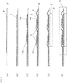
- the second lead frame 2 has such a shape as is shown in Figure 4(b) .
- the dot-dash-line shows the center line CL2 of the main body part 2x, and the direction thereof is the same as the direction in which the electric current that has gone in from the positive-electrode side outer part electrode 10 flows.
- the electric wiring part 5 has the portions 5a and 5b.
- the portion 5a electrically connects the semiconductor element 4a and the second island-shaped part 1 b.
- the portion 5b electrically connects the semiconductor element 4b and the third island-shaped part 1c.
- the semiconductor element 4a has, similarly to the semiconductor element 4b, such a shape as is shown in Figure 4(d) .
- the shapes of the semiconductor elements 4a and 4b are square in the present embodiment, but may be, for example, oblong.
- the width W4 of the semiconductor element 4a shows a width in the direction orthogonal to the center lines CL1-CL3.
- the first lead frame 1, the second lead frame 2, the electric wiring part 5 and the interlayer connecting part 6, and the semiconductor elements 4a and 4b after assembling are in such a position relationship as is shown in Figure 4(e) .
- the distance H1 between the upper face of the semiconductor element 4a and the upper face of the second lead frame 2 and the distance (the maximum distance) H2 between the upper face of the electric wiring part 5 and the upper face of the second lead frame 2 are equal to or more than 50 ⁇ m and are equal to or less than 500 ⁇ m.
- the distance H1 cannot be allowed to be smaller than the distance for which the thickness of the first lead frame 1 and the thickness of the semiconductor element 4a are added.
- the semiconductor elements 4a and 4b are configured with Si, SiC, GaN, GaAs or the like, and are for example transistors or diodes.
- the first insulation resin 7 and the second insulation resin 8 are, for example, configured with a publicly known material such that an inorganic component such as silica, AlN, Al 2 O 3 , BN or the like is mixed with a resin component such as an epoxy, a silicone, a polyimide or the like. It is desirable that the heat conduction rates of the first insulation resin 7 and the second insulation resin 8 be equal to or more than 2W/mK.
- the reason thereof is that, since the heat which is generated from the semiconductor elements 4a and 4b goes through the insulation resins of two layers of the first insulation resin 7 and the second insulation resin 8, in case the heat conduction rates of these are less than 2W/mK, then it becomes difficult to allow the heat which is generated from the semiconductor elements 4a and 4b to be sufficiently conducted to the heat radiating plate 3.
- the sealing resin 9 is, for example, configured with a publicly known material such that an inorganic component is mixed with a resin component such as an epoxy, a silicone, a polyimide or the like which becomes the main constituent.
- the second insulation resin 8 which has been processed so as to be a desired shape is laminated onto the second lead frame 2.
- the first lead frame 1 which has been prepared is disposed on the upper part of the object completed in the above-stated first step.
- the object completed in the above-stated fifth step is sealed with the sealing resin 9 by a publicly known transfer molding method.
- the heat radiating plate 3 onto which the first insulation resin 7 has been laminated is fixed to a predetermined position, and after that the first insulation resin 7 and the sealing resin 9 are allowed to harden utilizing a constant temperature bath or the like.
- the above-stated semiconductor apparatus can also lower noise which is apt to lead to malfunction of an external instrument, and can allow the performance of an inverter or the like which utilizes SiC, GaN, GaAs or the like and has high speed switching performance to be sufficiently exerted.
- first insulation resin 7 may be surface coating of the second lead frame 2
- second insulation resin 8 may be surface coating of the first lead frame 1 and/or the second lead frame 2
- first insulation resin 7 and the second insulation resin 8 may be integrated.
Landscapes
- Inverter Devices (AREA)
Claims (6)
- Dispositif à semi-conducteur comprenant :une première grille de connexion (1) qui est munie de premier et second éléments semi-conducteurs (4a, 4b),une seconde grille de connexion (2) qui est placée en parallèle à la première grille de connexion (1),une seconde résine d'isolement (8) qui est placée entre la première grille de connexion (1) et la seconde grille de connexion (2),une résine d'étanchéité (9) qui rend étanches les premier et second éléments semi-conducteurs (4a, 4b), la première grille de connexion (1) et la seconde grille de connexion (2),un composant de câblage électrique (5) qui est relié électriquement aux premier et second éléments semi-conducteurs (4a, 4b) et à la première grille de connexion (1),un composant de connexion entre couches (6) qui relie électriquement la première grille de connexion (1) et la seconde grille de connexion (2),caractérisé par
une plaque de rayonnement de chaleur (3) qui est placée parallèlement à la seconde grille de connexion (2), et
une première résine d'isolement (7) qui est placée entre la seconde grille de connexion (2) et la plaque de rayonnement de chaleur (3), dans lequel
la résine d'étanchéité (9) scelle la plaque de rayonnement de chaleur (3),
la première grille de connexion (1) comporte: un premier composant en forme d'îlot (1a) qui est muni du premier élément semi-conducteur (4a), un deuxième composant en forme d'îlot (1b) qui comporte une électrode de sortie (12) et qui est muni du second élément semi-conducteur (4b), ainsi qu'un troisième composant en forme d'îlot (1c) qui comporte l'une d'une électrode de composant externe du côté électrode positive (10) et d'une électrode de composant externe du côté électrode négatif (11),
la seconde grille de connexion (2) comporte une autre de l'électrode de composant externe du côté électrode positive (10) et de l'électrode de composant externe du côté électrode négative (11),
le composant de câblage électrique (5) relie électriquement le premier élément semi-conducteur (4a) et le deuxième composant en forme d'îlot (1b), et il relie électriquement le second élément semi-conducteur (4b) et le troisième composant en forme d'îlot (1c), et
le composant de connexion entre couches (6) relie électriquement le premier composant en forme d'îlot (1a) et la seconde grille de connexion (2). - Dispositif à semi-conducteur selon la revendication 1, dans lequel la distance entre la première grille de connexion (1) et la seconde grille de connexion (2) est supérieure ou égale à 50 µm et inférieure ou égale à 500 µm.
- Dispositif à semi-conducteur selon la revendication 1, dans lequel
le premier composant en forme d'îlot (1a) présente une forme d'un rectangle,
un organe formant corps principal (1bx) du deuxième composant en forme d'îlot (1b) présente la forme d'un rectangle à l'exception de l'électrode de sortie (12),
un organe formant corps principal (1cx) du troisième composant en forme d'îlot (1c) présente la forme d'un rectangle à l'exception de la première parmi l'électrode de composant externe du côté électrode positive (10) et l'électrode de composant externe du côté électrode négative (11),
un organe formant corps principal (2x) de la seconde grille de connexion (2) présente la forme d'un rectangle à l'exception de l'autre parmi l'électrode de composant externe du côté électrode positive (10) et l'électrode de composant externe du côté électrode négative (11),
l'axe central (CL1) du premier composant en forme d'îlot (1a), l'axe central (CL1) de l'organe formant corps principal (1bx) du deuxième composant en forme d'îlot (1b), l'axe central (CL1) de l'organe formant corps principal (1cx) du troisième composant en forme d'îlot (1c), l'axe central (CL2) de la seconde grille de connexion (2), l'axe central (CL3) du composant de câblage électrique (5) et l'axe central (CL3) du composant de connexion entre couches (6) sont disposés sur une même ligne, et
les centres (CP1) des premier et second éléments semi-conducteurs (4a, 4b) sont disposés sur la même ligne - Dispositif à semi-conducteur selon la revendication 1, dans lequel
le composant de câblage électrique (5) présente une forme de plaque plane cintrée,
l'organe formant corps principal (1bx) du deuxième composant en forme d'îlot (1b) présente la forme d'un rectangle à l'exception de l'électrode de sortie (12),
l'organe formant corps principal (1cx) du troisième composant en forme d'îlot (1c) présente la forme d'un rectangle à l'exception de la première parmi l'électrode de composant externe du côté électrode positive (10) et l'électrode de composant externe du côté électrode négative (11), et
la largeur de l'organe formant corps principal (1bx) du deuxième composant en forme d'îlot (1b) dans une direction orthogonale à la direction du courant électrique, la largeur de l'organe formant corps principal (1cx) du troisième composant en forme d'îlot (1c) dans une direction orthogonale à la direction du courant électrique, ainsi que la largeur d'une partie du composant de câblage électrique (5) qui est relié électriquement aux deuxième et troisième composants en forme d'îlot (1b, 1c) dans une direction orthogonale à la direction du courant électrique, sont égales. - Dispositif à semi-conducteur selon la revendication 1, dans lequel
le composant de connexion entre couches (6) présente la forme d'une plaque plane cintrée,
le premier composant en forme d'îlot (1a) présente la forme d'un rectangle, et
la largeur du premier composant en forme d'îlot (1a) dans une direction orthogonale à la direction du courant électrique et la largeur d'une partie du composant de connexion entre couches (6) qui est relié électriquement au premier composant en forme d'îlot (1a) dans une direction orthogonale à la direction du courant électrique, sont égales. - Dispositif à semi-conducteur selon la revendication 1, lequel est un dispositif à semi-conducteur utilisé pour un appareil de conversion de puissance électrique destiné à un moteur triphasé (104), dans lequel
l'électrode de sortie (12) est une électrode qui est reliée à l'une des électrodes de la phase U, de la phase V et de la phase W du moteur triphasé (104).
Applications Claiming Priority (2)
| Application Number | Priority Date | Filing Date | Title |
|---|---|---|---|
| JP2012150738 | 2012-07-04 | ||
| PCT/JP2013/003338 WO2014006814A1 (fr) | 2012-07-04 | 2013-05-27 | Dispositif semi-conducteur |
Publications (3)
| Publication Number | Publication Date |
|---|---|
| EP2871676A1 EP2871676A1 (fr) | 2015-05-13 |
| EP2871676A4 EP2871676A4 (fr) | 2015-12-16 |
| EP2871676B1 true EP2871676B1 (fr) | 2017-01-04 |
Family
ID=49881591
Family Applications (1)
| Application Number | Title | Priority Date | Filing Date |
|---|---|---|---|
| EP13813359.0A Not-in-force EP2871676B1 (fr) | 2012-07-04 | 2013-05-27 | Dispositif semi-conducteur |
Country Status (5)
| Country | Link |
|---|---|
| US (1) | US9379049B2 (fr) |
| EP (1) | EP2871676B1 (fr) |
| JP (1) | JP5967495B2 (fr) |
| CN (1) | CN104396011B (fr) |
| WO (1) | WO2014006814A1 (fr) |
Families Citing this family (13)
| Publication number | Priority date | Publication date | Assignee | Title |
|---|---|---|---|---|
| WO2014014012A1 (fr) * | 2012-07-19 | 2014-01-23 | 三菱電機株式会社 | Module semi-conducteur de puissance |
| WO2016002385A1 (fr) | 2014-07-03 | 2016-01-07 | 日産自動車株式会社 | Module de semi-conducteur de puissance en demi-pont et son procédé de fabrication |
| WO2016084241A1 (fr) * | 2014-11-28 | 2016-06-02 | 日産自動車株式会社 | Module à semi-conducteur de puissance en demi-pont et procédé pour sa fabrication |
| US10749443B2 (en) | 2017-01-13 | 2020-08-18 | Cree Fayetteville, Inc. | High power multilayer module having low inductance and fast switching for paralleling power devices |
| US11696417B2 (en) | 2017-01-13 | 2023-07-04 | Wolfspeed, Inc. | High power multilayer module having low inductance and fast switching for paralleling power devices |
| DE112018001927T5 (de) * | 2017-03-14 | 2019-12-19 | Rohm Co., Ltd. | Halbleiterbauelement |
| EP3909124A4 (fr) * | 2019-01-10 | 2022-10-26 | Wolfspeed, Inc. | Module multicouche haute puissance ayant une faible inductance et une commutation rapide pour mettre en parallèle des dispositifs de puissance |
| CN109755200B (zh) * | 2019-01-18 | 2020-03-24 | 上海大郡动力控制技术有限公司 | 一种功率半导体模块及电机控制器 |
| JP6976390B1 (ja) * | 2020-08-24 | 2021-12-08 | 三菱電機株式会社 | 半導体装置および電力変換装置 |
| EP4264349A1 (fr) * | 2020-12-17 | 2023-10-25 | Fremco A/S | Appareil d'installation de câble comprenant un dispositif d'entraînement remplaçable |
| DE102022207525A1 (de) | 2022-07-22 | 2024-01-25 | Vitesco Technologies Germany Gmbh | Leistungsmodul und Verfahren zur Herstellung desselben, Stromrichter mit einem Leistungsmodul |
| JP7848662B2 (ja) * | 2022-11-02 | 2026-04-21 | 株式会社デンソー | 半導体装置 |
| DE102024201718A1 (de) * | 2024-02-26 | 2025-08-28 | Robert Bosch Gesellschaft mit beschränkter Haftung | Leistungsmodulbrücke mit einer Anzahl von Leistungsmodulen |
Family Cites Families (13)
| Publication number | Priority date | Publication date | Assignee | Title |
|---|---|---|---|---|
| JPH06252332A (ja) | 1993-02-25 | 1994-09-09 | Fuji Electric Co Ltd | 電子デバイスの実装基板 |
| DE19581837T1 (de) * | 1994-11-10 | 1997-10-02 | Micron Technology Inc | Mehrlagiger Leitungsrahmen für eine Halbleitervorrichtung |
| WO1996031906A1 (fr) * | 1995-04-05 | 1996-10-10 | National Semiconductor Corporation | Grille de connexion multicouches |
| DE19900603A1 (de) * | 1999-01-11 | 2000-07-13 | Bosch Gmbh Robert | Elektronisches Halbleitermodul |
| JP3723869B2 (ja) * | 2001-03-30 | 2005-12-07 | 株式会社日立製作所 | 半導体装置 |
| JP3825309B2 (ja) * | 2001-11-30 | 2006-09-27 | 京セラ株式会社 | インバータ制御モジュール |
| JP2004221552A (ja) | 2002-12-26 | 2004-08-05 | Yamaha Motor Co Ltd | 電子基板、パワーモジュール、およびモータ駆動装置 |
| US7119437B2 (en) * | 2002-12-26 | 2006-10-10 | Yamaha Hatsudoki Kabushiki Kaisha | Electronic substrate, power module and motor driver |
| JP4277169B2 (ja) | 2003-01-06 | 2009-06-10 | 富士電機デバイステクノロジー株式会社 | 電力用半導体モジュール |
| JP2005236108A (ja) | 2004-02-20 | 2005-09-02 | Toyota Motor Corp | 半導体装置 |
| JP2007116013A (ja) * | 2005-10-24 | 2007-05-10 | Renesas Technology Corp | 半導体装置及びそれを用いた電源装置 |
| WO2012011210A1 (fr) | 2010-07-22 | 2012-01-26 | パナソニック株式会社 | Dispositif semi-conducteur et son procédé de fabrication |
| JP2010258485A (ja) | 2010-08-24 | 2010-11-11 | Renesas Electronics Corp | 半導体装置 |
-
2013
- 2013-05-27 JP JP2014523565A patent/JP5967495B2/ja not_active Expired - Fee Related
- 2013-05-27 WO PCT/JP2013/003338 patent/WO2014006814A1/fr not_active Ceased
- 2013-05-27 CN CN201380033792.6A patent/CN104396011B/zh not_active Expired - Fee Related
- 2013-05-27 US US14/409,135 patent/US9379049B2/en not_active Expired - Fee Related
- 2013-05-27 EP EP13813359.0A patent/EP2871676B1/fr not_active Not-in-force
Non-Patent Citations (1)
| Title |
|---|
| None * |
Also Published As
| Publication number | Publication date |
|---|---|
| JP5967495B2 (ja) | 2016-08-10 |
| WO2014006814A1 (fr) | 2014-01-09 |
| EP2871676A4 (fr) | 2015-12-16 |
| JPWO2014006814A1 (ja) | 2016-06-02 |
| US9379049B2 (en) | 2016-06-28 |
| CN104396011A (zh) | 2015-03-04 |
| EP2871676A1 (fr) | 2015-05-13 |
| CN104396011B (zh) | 2017-06-06 |
| US20150194372A1 (en) | 2015-07-09 |
Similar Documents
| Publication | Publication Date | Title |
|---|---|---|
| EP2871676B1 (fr) | Dispositif semi-conducteur | |
| US11810775B2 (en) | High power module package structures | |
| US7045884B2 (en) | Semiconductor device package | |
| US20160315038A1 (en) | Semiconductor module | |
| JP7199167B2 (ja) | パワー半導体モジュール、電力変換装置、およびパワー半導体モジュールの製造方法 | |
| EP2851951B1 (fr) | Procédé de fabrication d'un dispositif à semi-conducteurs, et dispositif à semi-conducteurs | |
| JP2007234690A (ja) | パワー半導体モジュール | |
| US10804186B2 (en) | Semiconductor module and power converter | |
| US11973063B2 (en) | Semiconductor package with low parasitic connection to passive device | |
| US12293955B2 (en) | High power module package structures | |
| CN110178304A (zh) | 半导体装置 | |
| CN110880488A (zh) | 半导体装置及电力转换装置 | |
| US11996344B2 (en) | Semiconductor device | |
| JP2018073923A (ja) | 電力用半導体装置、電力用半導体装置の製造方法および電力変換装置 | |
| WO2025091326A1 (fr) | Structure de borne pour conditionnement de semi-conducteur de puissance | |
| US20240356322A1 (en) | Signal loop busbars and semiconductor power modules including the same and processes of implementing the same | |
| US20260089898A1 (en) | Cooling apparatus for power modules | |
| US20260068691A1 (en) | Semiconductor Package with Selective Surface Roughening | |
| JP7827973B2 (ja) | 半導体装置 | |
| US20250372520A1 (en) | Power discrete package having symmetric pinouts and process of implementing the same | |
| US20240429147A1 (en) | Semiconductor apparatus | |
| JP2025145248A (ja) | 半導体装置およびその製造方法 | |
| JP2025122815A (ja) | 半導体モジュール及び車両 | |
| JP2026054024A (ja) | パワーモジュール、パワーモジュールの製造方法、および電力変換装置 | |
| CN120473453A (zh) | 具有包括电源端子的多层级金属框架的功率模块 |
Legal Events
| Date | Code | Title | Description |
|---|---|---|---|
| PUAI | Public reference made under article 153(3) epc to a published international application that has entered the european phase |
Free format text: ORIGINAL CODE: 0009012 |
|
| 17P | Request for examination filed |
Effective date: 20141215 |
|
| AK | Designated contracting states |
Kind code of ref document: A1 Designated state(s): AL AT BE BG CH CY CZ DE DK EE ES FI FR GB GR HR HU IE IS IT LI LT LU LV MC MK MT NL NO PL PT RO RS SE SI SK SM TR |
|
| AX | Request for extension of the european patent |
Extension state: BA ME |
|
| DAX | Request for extension of the european patent (deleted) | ||
| RA4 | Supplementary search report drawn up and despatched (corrected) |
Effective date: 20151116 |
|
| RIC1 | Information provided on ipc code assigned before grant |
Ipc: H01L 23/31 20060101ALI20151110BHEP Ipc: H01L 23/433 20060101ALI20151110BHEP Ipc: H01L 25/18 20060101ALI20151110BHEP Ipc: H01L 23/495 20060101ALI20151110BHEP Ipc: H02M 7/48 20070101ALI20151110BHEP Ipc: H01L 25/07 20060101AFI20151110BHEP |
|
| GRAP | Despatch of communication of intention to grant a patent |
Free format text: ORIGINAL CODE: EPIDOSNIGR1 |
|
| INTG | Intention to grant announced |
Effective date: 20160729 |
|
| GRAS | Grant fee paid |
Free format text: ORIGINAL CODE: EPIDOSNIGR3 |
|
| GRAA | (expected) grant |
Free format text: ORIGINAL CODE: 0009210 |
|
| RIN1 | Information on inventor provided before grant (corrected) |
Inventor name: IKEUCHI, HIROKI |
|
| AK | Designated contracting states |
Kind code of ref document: B1 Designated state(s): AL AT BE BG CH CY CZ DE DK EE ES FI FR GB GR HR HU IE IS IT LI LT LU LV MC MK MT NL NO PL PT RO RS SE SI SK SM TR |
|
| REG | Reference to a national code |
Ref country code: GB Ref legal event code: FG4D |
|
| REG | Reference to a national code |
Ref country code: CH Ref legal event code: EP |
|
| REG | Reference to a national code |
Ref country code: AT Ref legal event code: REF Ref document number: 860000 Country of ref document: AT Kind code of ref document: T Effective date: 20170115 |
|
| REG | Reference to a national code |
Ref country code: IE Ref legal event code: FG4D |
|
| REG | Reference to a national code |
Ref country code: DE Ref legal event code: R096 Ref document number: 602013016308 Country of ref document: DE |
|
| REG | Reference to a national code |
Ref country code: LT Ref legal event code: MG4D Ref country code: NL Ref legal event code: MP Effective date: 20170104 |
|
| REG | Reference to a national code |
Ref country code: AT Ref legal event code: MK05 Ref document number: 860000 Country of ref document: AT Kind code of ref document: T Effective date: 20170104 |
|
| PG25 | Lapsed in a contracting state [announced via postgrant information from national office to epo] |
Ref country code: NL Free format text: LAPSE BECAUSE OF FAILURE TO SUBMIT A TRANSLATION OF THE DESCRIPTION OR TO PAY THE FEE WITHIN THE PRESCRIBED TIME-LIMIT Effective date: 20170104 |
|
| PG25 | Lapsed in a contracting state [announced via postgrant information from national office to epo] |
Ref country code: FI Free format text: LAPSE BECAUSE OF FAILURE TO SUBMIT A TRANSLATION OF THE DESCRIPTION OR TO PAY THE FEE WITHIN THE PRESCRIBED TIME-LIMIT Effective date: 20170104 Ref country code: LT Free format text: LAPSE BECAUSE OF FAILURE TO SUBMIT A TRANSLATION OF THE DESCRIPTION OR TO PAY THE FEE WITHIN THE PRESCRIBED TIME-LIMIT Effective date: 20170104 Ref country code: IS Free format text: LAPSE BECAUSE OF FAILURE TO SUBMIT A TRANSLATION OF THE DESCRIPTION OR TO PAY THE FEE WITHIN THE PRESCRIBED TIME-LIMIT Effective date: 20170504 Ref country code: GR Free format text: LAPSE BECAUSE OF FAILURE TO SUBMIT A TRANSLATION OF THE DESCRIPTION OR TO PAY THE FEE WITHIN THE PRESCRIBED TIME-LIMIT Effective date: 20170405 Ref country code: NO Free format text: LAPSE BECAUSE OF FAILURE TO SUBMIT A TRANSLATION OF THE DESCRIPTION OR TO PAY THE FEE WITHIN THE PRESCRIBED TIME-LIMIT Effective date: 20170404 Ref country code: HR Free format text: LAPSE BECAUSE OF FAILURE TO SUBMIT A TRANSLATION OF THE DESCRIPTION OR TO PAY THE FEE WITHIN THE PRESCRIBED TIME-LIMIT Effective date: 20170104 |
|
| PG25 | Lapsed in a contracting state [announced via postgrant information from national office to epo] |
Ref country code: PL Free format text: LAPSE BECAUSE OF FAILURE TO SUBMIT A TRANSLATION OF THE DESCRIPTION OR TO PAY THE FEE WITHIN THE PRESCRIBED TIME-LIMIT Effective date: 20170104 Ref country code: PT Free format text: LAPSE BECAUSE OF FAILURE TO SUBMIT A TRANSLATION OF THE DESCRIPTION OR TO PAY THE FEE WITHIN THE PRESCRIBED TIME-LIMIT Effective date: 20170504 Ref country code: RS Free format text: LAPSE BECAUSE OF FAILURE TO SUBMIT A TRANSLATION OF THE DESCRIPTION OR TO PAY THE FEE WITHIN THE PRESCRIBED TIME-LIMIT Effective date: 20170104 Ref country code: ES Free format text: LAPSE BECAUSE OF FAILURE TO SUBMIT A TRANSLATION OF THE DESCRIPTION OR TO PAY THE FEE WITHIN THE PRESCRIBED TIME-LIMIT Effective date: 20170104 Ref country code: LV Free format text: LAPSE BECAUSE OF FAILURE TO SUBMIT A TRANSLATION OF THE DESCRIPTION OR TO PAY THE FEE WITHIN THE PRESCRIBED TIME-LIMIT Effective date: 20170104 Ref country code: LU Free format text: LAPSE BECAUSE OF NON-PAYMENT OF DUE FEES Effective date: 20170531 Ref country code: AT Free format text: LAPSE BECAUSE OF FAILURE TO SUBMIT A TRANSLATION OF THE DESCRIPTION OR TO PAY THE FEE WITHIN THE PRESCRIBED TIME-LIMIT Effective date: 20170104 Ref country code: SE Free format text: LAPSE BECAUSE OF FAILURE TO SUBMIT A TRANSLATION OF THE DESCRIPTION OR TO PAY THE FEE WITHIN THE PRESCRIBED TIME-LIMIT Effective date: 20170104 Ref country code: BG Free format text: LAPSE BECAUSE OF FAILURE TO SUBMIT A TRANSLATION OF THE DESCRIPTION OR TO PAY THE FEE WITHIN THE PRESCRIBED TIME-LIMIT Effective date: 20170404 |
|
| REG | Reference to a national code |
Ref country code: DE Ref legal event code: R097 Ref document number: 602013016308 Country of ref document: DE |
|
| PG25 | Lapsed in a contracting state [announced via postgrant information from national office to epo] |
Ref country code: CZ Free format text: LAPSE BECAUSE OF FAILURE TO SUBMIT A TRANSLATION OF THE DESCRIPTION OR TO PAY THE FEE WITHIN THE PRESCRIBED TIME-LIMIT Effective date: 20170104 Ref country code: IT Free format text: LAPSE BECAUSE OF FAILURE TO SUBMIT A TRANSLATION OF THE DESCRIPTION OR TO PAY THE FEE WITHIN THE PRESCRIBED TIME-LIMIT Effective date: 20170104 Ref country code: SK Free format text: LAPSE BECAUSE OF FAILURE TO SUBMIT A TRANSLATION OF THE DESCRIPTION OR TO PAY THE FEE WITHIN THE PRESCRIBED TIME-LIMIT Effective date: 20170104 Ref country code: EE Free format text: LAPSE BECAUSE OF FAILURE TO SUBMIT A TRANSLATION OF THE DESCRIPTION OR TO PAY THE FEE WITHIN THE PRESCRIBED TIME-LIMIT Effective date: 20170104 Ref country code: RO Free format text: LAPSE BECAUSE OF FAILURE TO SUBMIT A TRANSLATION OF THE DESCRIPTION OR TO PAY THE FEE WITHIN THE PRESCRIBED TIME-LIMIT Effective date: 20170104 |
|
| PLBE | No opposition filed within time limit |
Free format text: ORIGINAL CODE: 0009261 |
|
| STAA | Information on the status of an ep patent application or granted ep patent |
Free format text: STATUS: NO OPPOSITION FILED WITHIN TIME LIMIT |
|
| PG25 | Lapsed in a contracting state [announced via postgrant information from national office to epo] |
Ref country code: DK Free format text: LAPSE BECAUSE OF FAILURE TO SUBMIT A TRANSLATION OF THE DESCRIPTION OR TO PAY THE FEE WITHIN THE PRESCRIBED TIME-LIMIT Effective date: 20170104 Ref country code: SM Free format text: LAPSE BECAUSE OF FAILURE TO SUBMIT A TRANSLATION OF THE DESCRIPTION OR TO PAY THE FEE WITHIN THE PRESCRIBED TIME-LIMIT Effective date: 20170104 |
|
| REG | Reference to a national code |
Ref country code: CH Ref legal event code: PL |
|
| GBPC | Gb: european patent ceased through non-payment of renewal fee |
Effective date: 20170527 |
|
| PG25 | Lapsed in a contracting state [announced via postgrant information from national office to epo] |
Ref country code: MC Free format text: LAPSE BECAUSE OF FAILURE TO SUBMIT A TRANSLATION OF THE DESCRIPTION OR TO PAY THE FEE WITHIN THE PRESCRIBED TIME-LIMIT Effective date: 20170104 |
|
| REG | Reference to a national code |
Ref country code: IE Ref legal event code: MM4A |
|
| PG25 | Lapsed in a contracting state [announced via postgrant information from national office to epo] |
Ref country code: SI Free format text: LAPSE BECAUSE OF FAILURE TO SUBMIT A TRANSLATION OF THE DESCRIPTION OR TO PAY THE FEE WITHIN THE PRESCRIBED TIME-LIMIT Effective date: 20170104 Ref country code: LI Free format text: LAPSE BECAUSE OF NON-PAYMENT OF DUE FEES Effective date: 20170531 Ref country code: CH Free format text: LAPSE BECAUSE OF NON-PAYMENT OF DUE FEES Effective date: 20170531 |
|
| REG | Reference to a national code |
Ref country code: FR Ref legal event code: ST Effective date: 20180131 |
|
| PG25 | Lapsed in a contracting state [announced via postgrant information from national office to epo] |
Ref country code: LU Free format text: LAPSE BECAUSE OF NON-PAYMENT OF DUE FEES Effective date: 20170527 |
|
| REG | Reference to a national code |
Ref country code: BE Ref legal event code: MM Effective date: 20170531 |
|
| PG25 | Lapsed in a contracting state [announced via postgrant information from national office to epo] |
Ref country code: IE Free format text: LAPSE BECAUSE OF NON-PAYMENT OF DUE FEES Effective date: 20170527 Ref country code: GB Free format text: LAPSE BECAUSE OF NON-PAYMENT OF DUE FEES Effective date: 20170527 |
|
| PG25 | Lapsed in a contracting state [announced via postgrant information from national office to epo] |
Ref country code: FR Free format text: LAPSE BECAUSE OF NON-PAYMENT OF DUE FEES Effective date: 20170531 |
|
| PG25 | Lapsed in a contracting state [announced via postgrant information from national office to epo] |
Ref country code: BE Free format text: LAPSE BECAUSE OF NON-PAYMENT OF DUE FEES Effective date: 20170531 |
|
| PG25 | Lapsed in a contracting state [announced via postgrant information from national office to epo] |
Ref country code: MT Free format text: LAPSE BECAUSE OF NON-PAYMENT OF DUE FEES Effective date: 20170527 |
|
| PG25 | Lapsed in a contracting state [announced via postgrant information from national office to epo] |
Ref country code: HU Free format text: LAPSE BECAUSE OF FAILURE TO SUBMIT A TRANSLATION OF THE DESCRIPTION OR TO PAY THE FEE WITHIN THE PRESCRIBED TIME-LIMIT; INVALID AB INITIO Effective date: 20130527 |
|
| PG25 | Lapsed in a contracting state [announced via postgrant information from national office to epo] |
Ref country code: CY Free format text: LAPSE BECAUSE OF FAILURE TO SUBMIT A TRANSLATION OF THE DESCRIPTION OR TO PAY THE FEE WITHIN THE PRESCRIBED TIME-LIMIT Effective date: 20170104 |
|
| PG25 | Lapsed in a contracting state [announced via postgrant information from national office to epo] |
Ref country code: MK Free format text: LAPSE BECAUSE OF FAILURE TO SUBMIT A TRANSLATION OF THE DESCRIPTION OR TO PAY THE FEE WITHIN THE PRESCRIBED TIME-LIMIT Effective date: 20170104 |
|
| PG25 | Lapsed in a contracting state [announced via postgrant information from national office to epo] |
Ref country code: TR Free format text: LAPSE BECAUSE OF FAILURE TO SUBMIT A TRANSLATION OF THE DESCRIPTION OR TO PAY THE FEE WITHIN THE PRESCRIBED TIME-LIMIT Effective date: 20170104 |
|
| PG25 | Lapsed in a contracting state [announced via postgrant information from national office to epo] |
Ref country code: AL Free format text: LAPSE BECAUSE OF FAILURE TO SUBMIT A TRANSLATION OF THE DESCRIPTION OR TO PAY THE FEE WITHIN THE PRESCRIBED TIME-LIMIT Effective date: 20170104 |
|
| PGFP | Annual fee paid to national office [announced via postgrant information from national office to epo] |
Ref country code: DE Payment date: 20230519 Year of fee payment: 11 |
|
| REG | Reference to a national code |
Ref country code: DE Ref legal event code: R079 Ref document number: 602013016308 Country of ref document: DE Free format text: PREVIOUS MAIN CLASS: H01L0025070000 Ipc: H10D0080200000 |
|
| REG | Reference to a national code |
Ref country code: DE Ref legal event code: R119 Ref document number: 602013016308 Country of ref document: DE |
|
| PG25 | Lapsed in a contracting state [announced via postgrant information from national office to epo] |
Ref country code: DE Free format text: LAPSE BECAUSE OF NON-PAYMENT OF DUE FEES Effective date: 20241203 |