EP2872948B1 - Compositions pour traitement anti-affaissement de motif comprenant des additifs géminés - Google Patents
Compositions pour traitement anti-affaissement de motif comprenant des additifs géminés Download PDFInfo
- Publication number
- EP2872948B1 EP2872948B1 EP13816602.0A EP13816602A EP2872948B1 EP 2872948 B1 EP2872948 B1 EP 2872948B1 EP 13816602 A EP13816602 A EP 13816602A EP 2872948 B1 EP2872948 B1 EP 2872948B1
- Authority
- EP
- European Patent Office
- Prior art keywords
- linear
- photoresist
- branched
- optionally
- substrate
- Prior art date
- Legal status (The legal status is an assumption and is not a legal conclusion. Google has not performed a legal analysis and makes no representation as to the accuracy of the status listed.)
- Not-in-force
Links
- 0 C*[*+]1*N(*I)*1 Chemical compound C*[*+]1*N(*I)*1 0.000 description 1
- YNQLUTRBYVCPMQ-UHFFFAOYSA-N CCc1ccccc1 Chemical compound CCc1ccccc1 YNQLUTRBYVCPMQ-UHFFFAOYSA-N 0.000 description 1
- JYAMXLXEUYQPKX-UHFFFAOYSA-N C[N]1(CCCC[N]2(C)CCCC2)CCCC1 Chemical compound C[N]1(CCCC[N]2(C)CCCC2)CCCC1 JYAMXLXEUYQPKX-UHFFFAOYSA-N 0.000 description 1
Images

Classifications
-
- G—PHYSICS
- G03—PHOTOGRAPHY; CINEMATOGRAPHY; ANALOGOUS TECHNIQUES USING WAVES OTHER THAN OPTICAL WAVES; ELECTROGRAPHY; HOLOGRAPHY
- G03F—PHOTOMECHANICAL PRODUCTION OF TEXTURED OR PATTERNED SURFACES, e.g. FOR PRINTING, FOR PROCESSING OF SEMICONDUCTOR DEVICES; MATERIALS THEREFOR; ORIGINALS THEREFOR; APPARATUS SPECIALLY ADAPTED THEREFOR
- G03F7/00—Photomechanical, e.g. photolithographic, production of textured or patterned surfaces, e.g. printing surfaces; Materials therefor, e.g. comprising photoresists; Apparatus specially adapted therefor
- G03F7/26—Processing photosensitive materials; Apparatus therefor
- G03F7/30—Imagewise removal using liquid means
- G03F7/32—Liquid compositions therefor, e.g. developers
-
- C—CHEMISTRY; METALLURGY
- C11—ANIMAL OR VEGETABLE OILS, FATS, FATTY SUBSTANCES OR WAXES; FATTY ACIDS THEREFROM; DETERGENTS; CANDLES
- C11D—DETERGENT COMPOSITIONS; USE OF SINGLE SUBSTANCES AS DETERGENTS; SOAP OR SOAP-MAKING; RESIN SOAPS; RECOVERY OF GLYCEROL
- C11D1/00—Detergent compositions based essentially on surface-active compounds; Use of these compounds as a detergent
- C11D1/008—Polymeric surface-active agents
-
- C—CHEMISTRY; METALLURGY
- C11—ANIMAL OR VEGETABLE OILS, FATS, FATTY SUBSTANCES OR WAXES; FATTY ACIDS THEREFROM; DETERGENTS; CANDLES
- C11D—DETERGENT COMPOSITIONS; USE OF SINGLE SUBSTANCES AS DETERGENTS; SOAP OR SOAP-MAKING; RESIN SOAPS; RECOVERY OF GLYCEROL
- C11D1/00—Detergent compositions based essentially on surface-active compounds; Use of these compounds as a detergent
- C11D1/38—Cationic compounds
- C11D1/40—Monoamines or polyamines; Salts thereof
-
- C—CHEMISTRY; METALLURGY
- C11—ANIMAL OR VEGETABLE OILS, FATS, FATTY SUBSTANCES OR WAXES; FATTY ACIDS THEREFROM; DETERGENTS; CANDLES
- C11D—DETERGENT COMPOSITIONS; USE OF SINGLE SUBSTANCES AS DETERGENTS; SOAP OR SOAP-MAKING; RESIN SOAPS; RECOVERY OF GLYCEROL
- C11D1/00—Detergent compositions based essentially on surface-active compounds; Use of these compounds as a detergent
- C11D1/38—Cationic compounds
- C11D1/62—Quaternary ammonium compounds
-
- G—PHYSICS
- G03—PHOTOGRAPHY; CINEMATOGRAPHY; ANALOGOUS TECHNIQUES USING WAVES OTHER THAN OPTICAL WAVES; ELECTROGRAPHY; HOLOGRAPHY
- G03F—PHOTOMECHANICAL PRODUCTION OF TEXTURED OR PATTERNED SURFACES, e.g. FOR PRINTING, FOR PROCESSING OF SEMICONDUCTOR DEVICES; MATERIALS THEREFOR; ORIGINALS THEREFOR; APPARATUS SPECIALLY ADAPTED THEREFOR
- G03F7/00—Photomechanical, e.g. photolithographic, production of textured or patterned surfaces, e.g. printing surfaces; Materials therefor, e.g. comprising photoresists; Apparatus specially adapted therefor
- G03F7/20—Exposure; Apparatus therefor
- G03F7/2041—Exposure; Apparatus therefor in the presence of a fluid, e.g. immersion; using fluid cooling means
-
- G—PHYSICS
- G03—PHOTOGRAPHY; CINEMATOGRAPHY; ANALOGOUS TECHNIQUES USING WAVES OTHER THAN OPTICAL WAVES; ELECTROGRAPHY; HOLOGRAPHY
- G03F—PHOTOMECHANICAL PRODUCTION OF TEXTURED OR PATTERNED SURFACES, e.g. FOR PRINTING, FOR PROCESSING OF SEMICONDUCTOR DEVICES; MATERIALS THEREFOR; ORIGINALS THEREFOR; APPARATUS SPECIALLY ADAPTED THEREFOR
- G03F7/00—Photomechanical, e.g. photolithographic, production of textured or patterned surfaces, e.g. printing surfaces; Materials therefor, e.g. comprising photoresists; Apparatus specially adapted therefor
- G03F7/26—Processing photosensitive materials; Apparatus therefor
- G03F7/30—Imagewise removal using liquid means
- G03F7/32—Liquid compositions therefor, e.g. developers
- G03F7/322—Aqueous alkaline compositions
-
- G—PHYSICS
- G03—PHOTOGRAPHY; CINEMATOGRAPHY; ANALOGOUS TECHNIQUES USING WAVES OTHER THAN OPTICAL WAVES; ELECTROGRAPHY; HOLOGRAPHY
- G03F—PHOTOMECHANICAL PRODUCTION OF TEXTURED OR PATTERNED SURFACES, e.g. FOR PRINTING, FOR PROCESSING OF SEMICONDUCTOR DEVICES; MATERIALS THEREFOR; ORIGINALS THEREFOR; APPARATUS SPECIALLY ADAPTED THEREFOR
- G03F7/00—Photomechanical, e.g. photolithographic, production of textured or patterned surfaces, e.g. printing surfaces; Materials therefor, e.g. comprising photoresists; Apparatus specially adapted therefor
- G03F7/26—Processing photosensitive materials; Apparatus therefor
- G03F7/40—Treatment after imagewise removal, e.g. baking
-
- H—ELECTRICITY
- H10—SEMICONDUCTOR DEVICES; ELECTRIC SOLID-STATE DEVICES NOT OTHERWISE PROVIDED FOR
- H10P—GENERIC PROCESSES OR APPARATUS FOR THE MANUFACTURE OR TREATMENT OF DEVICES COVERED BY CLASS H10
- H10P76/00—Manufacture or treatment of masks on semiconductor bodies, e.g. by lithography or photolithography
- H10P76/20—Manufacture or treatment of masks on semiconductor bodies, e.g. by lithography or photolithography of masks comprising organic materials
- H10P76/204—Manufacture or treatment of masks on semiconductor bodies, e.g. by lithography or photolithography of masks comprising organic materials of organic photoresist masks
- H10P76/2041—Photolithographic processes
-
- C—CHEMISTRY; METALLURGY
- C11—ANIMAL OR VEGETABLE OILS, FATS, FATTY SUBSTANCES OR WAXES; FATTY ACIDS THEREFROM; DETERGENTS; CANDLES
- C11D—DETERGENT COMPOSITIONS; USE OF SINGLE SUBSTANCES AS DETERGENTS; SOAP OR SOAP-MAKING; RESIN SOAPS; RECOVERY OF GLYCEROL
- C11D2111/00—Cleaning compositions characterised by the objects to be cleaned; Cleaning compositions characterised by non-standard cleaning or washing processes
- C11D2111/10—Objects to be cleaned
- C11D2111/14—Hard surfaces
- C11D2111/22—Electronic devices, e.g. PCBs or semiconductors
Definitions
- the present invention is directed to a composition useful in processes for manufacturing integrated circuits devices, optical devices, micromachines and mechanical precision devices, in particular for developing photoresists and post etch residue removal to avoid anti pattern collapse.
- patterned material layers like patterned photoresist layers, patterned barrier material layers containing or consisting of titanium nitride, tantalum or tantalum nitride, patterned multi-stack material layers containing or consisting of stacks e.g. of alternating polysilicon and silicon dioxide layers, and patterned dielectric material layers containing or consisting of silicon dioxide or low-k or ultra-low-k dielectric materials are produced by photolithographic techniques.
- patterned material layers comprise structures of dimensions even below 22 nm with high aspect ratios.
- Photolithography is a method in which a pattern on a mask is projected onto a substrate such as a semiconductor wafer.
- Semiconductor photolithography typically includes the step of applying a layer of a photoresist on a top surface of the semiconductor substrate and exposing the photoresist to actinic radiation, in particular UV radiation of a wavelength of, for example, 193 nm, through the mask.
- actinic radiation in particular UV radiation of a wavelength of, for example, 193 nm
- immersion photolithography has been developed as a resolution enhancement technique.
- the air gap between the final lens of the optical system and the photoresist surface is replaced by a liquid medium that has a refractive index greater than one, e.g., ultra pure water with a refractive index of 1.44 for the wavelength of 193 nm.
- a barrier coating or a water resistant photoresist must be used.
- Beside the 193nm-immersion lithography other illumination techniques with significant shorter wavelength are considered to be solutions to fulfil the needs of further downscaling of the to be printed feature sizes of 20nm node and below.
- EUV Extreme Ultraviolet
- An optional post-exposure bake is often performed to allow the exposed photoresist polymers to cleave.
- the substrate including the cleaved polymer photoresist is then transferred to a developing chamber to remove the exposed photoresist, which is soluble in aqueous developing compositions.
- developing compositions comprise tetraalkylammonium hydroxides, such as but not limited to tetramethylammonium hydroxide (TMAH) are applied to the resist surface in the form of a puddle to develop the exposed photoresist.
- TMAH tetramethylammonium hydroxide
- a deionized water rinse is then applied to the substrate to remove the dissolved polymers of the photoresists.
- the substrate is then sent to a spin drying process. Thereafter, the substrate can be transferred to the next process step, which may include a hard bake process to remove any moisture from the photoresist surface.
- photoresist patterns are required to include relatively thin and tall structures or features of photoresists, i.e., features having a high aspect ratio, on the substrate. These structures may suffer from bending and/or collapsing (so called pattern collapse), in particular, during the spin dry process, due to excessive capillary forces of the liquid or solution of the rinsing liquid deionized water remaining from the chemical rinse and spin dry processes and being disposed between adjacent photoresist features.
- pattern collapse bending and/or collapsing
- the calculated maximum stress ⁇ between small features caused by the capillary forces can be described according to Namatsu et al. Appl. Phys.
- LER line edge roughness
- LWR line width roughness
- Watermarks may form on the photoresist as the deionized water or rinse liquid cannot be spun off from the hydrophobic surface of the photoresist.
- the photoresist may be hydrophobic particularly in areas of isolated, or non-dense, patterning. The watermarks have a harmful effect on yield and IC device performance.
- EP 1 553 454 A2 discloses the use of cetylmethylammonium, stearylmethylammonium, cetyltrimethylammonium, stearyltrimethylammonium, distearyldimethylammonium, stearyldimethylbenzylammoium, dodecylmethylammonium, dodecyltrimethylammonium, benzylmethylammonium, benzyltrimethylammonium, and benzalkonium chloride as cationic surfactants in rinsing compositions for patterns having line-space dimensions of 90 nm.
- US 6670107 B2 discloses a method for the reduction of defects in an electronic device comprising of cationic and non-ionic surfactants in concentration less than or equal to the critical micelle concentration.
- US 2010/0248164 A1 discloses a rinse solution for preventing pattern collapse consisting of an anionic surfactant, an amine and water.
- Patent application US 2000/53172 A1 discloses that the acetylenic diol-type of surfactant solutions prevent pattern collapse by making the surface of a photoresist hydrophilic thus improving the wettability of the rinse or solution.
- pattern collapse may generally be caused by:
- the present invention mainly addresses the problems under Lit. A and B, i.e. to prevent swelling of the photoresist and to prevent pattern collapse by using a defect reduction rinse after the development of the photoresist.
- the compounds according to the present invention shall allow for the immersion photolithography of photoresist layers, the developing of the photoresist layers exposed to actinic radiation through a mask, the chemical rinse of patterned material layers comprising patterns with a high aspect ratio and line-space dimensions of 50 nm and less, in particular, of 32 nm and less, especially, of 22 nm and less, without causing pattern collapse, an increase of LER, LWR and watermark defects.
- the components according to the present invention should allow for a significant reduction of LER and LWR by smoothing the roughness of the surfaces of the developed photoresist patterns. It should also allow for the efficient prevention and/or the removal of watermark defects on patterned material layers, in particular, but not limited to photoresist patterns. Furthermore it should allow for the efficient removal of particles in order to achieve a significant defect reduction on patterned material layers.
- the components according to the present invention should also allow for a significant reduction of photoresist swelling.
- a first embodiment of the present invention is the use of gemini additives of the general formula I in compositions for treating semiconductor substrates: wherein:
- Gemini additives according to the invention allowed for the immersion photolithography of photoresist layers, the developing of photoresist layers exposed to actinic radiation through a mask, the cleaning of patterned material layers, or combinations thereof.
- the surfactants according to the invention are particularly useful for pattern developing or cleaning developed photoresist layers comprising patterns having line-space dimensions of 50 nm or less, particularly of 32 nm or less and, most particularly 22 nm or less.
- the gemini additives according to the invention are particularly useful for aspect ratios greater or equal 2 in the case of photoresist structures, and, in particular, greater or equal 10 in the case of non-photoresist structures, without causing pattern collapse, line edge roughness (LER), line width roughness (LWR) and watermark defects in the photoresist case and anti pattern collapse, defect reduction and cleaning in the high aspect ratio case.
- compositions comprising the gemini additives according to the present invention are generally useful for avoiding anti pattern collapse of photoresist structures as well as of non-photoresist patterns with high aspect ratios (HARS, typical aspect ratios are greater or equal 10).
- the method of the invention allowed for a significant reduction of LER and LWR by smoothing the roughness of the surfaces of the developed photoresist patterns, for the efficient prevention and/or the removal of watermark defects not only on photoresist patterns, but also on other patterned material layers, and the efficient removal of particles whereby a significant defect reduction not only on photoresist patterns but also on other patterned material layers could be achieved.
- gemini additives in the developer compositions could prevent swelling of the photoresist layer due to reduced diffusion. This also reduces the risk of pattern collapse of the photoresist during the subsequent steps.
- the use of the gemini additives in the developer solutions enables tuning surface tension and the interaction of the developer solution with the photo resist.
- the gemini-surfactants of the general formula I may advantageously used in the process for manufacturing IC devices but also for other devices to be provided with patterned structures of nm dimensions.
- the gemini additives may particularly be used in photoresist developing compositions as well as in cleaning or rinsing compositions during the photolithographic process in order to pattern semiconductor substrates.
- rinsing and cleaning are use synonymously for the defect reduction rinsing step after the photoresist developing step.
- the substrate is a semiconductor substrate, more preferably a silicon wafer including a silicon-gallium wafer, which wafers are customarily used for manufacturing IC devices, in particular IC devices comprising ICs having LSI, VLSI and ULSI.
- the composition is particularly suitable for treating substrates having patterned material layers having line-space dimensions of 50 nm and less, in particular, 32 nm and less and, especially, 22 nm and less, i.e. patterned material layers for the sub-22 nm technology nodes.
- the patterned material layers preferably have ratios above 2, preferably above 10, even more preferably above 50.
- the ratios are above 2 and when they comprise or consist of non-photoresist structures the ratios are above 10.
- the aspect ratio is in the range of up to 75, as for example, for 15 nm flash devices.
- composition according to the present invention may be applied to substrates of any patterned material as long as structures tend to collapse due to their geometry.
- the patterned material layers may be any suitable material layers.
- the patterned material layers may be any suitable material layers.
- the cleaning/rinsing compositions as well as the developer compositions comprising the gemini additives are preferably aqueous solutions.
- the cleaning/rinsing compositions are used at a pH of about 6 to about 8.
- the developing compositions are used at a pH of 8 or more, preferably at a pH of from 9 to 14.
- Aqueous means that the solvent comprises water, preferably deionized water and, most preferably ultrapure water as the main solvent.
- the aqueous composition may contain water-miscible polar organic solvents, albeit only in such minor amounts that do not jeopardize the aqueous nature of the composition.
- the solvent essentially consists of water, preferably deionized water and, most preferably ultrapure water.
- ultrapure water with concentration of 5 ppt (ng/kg), or better, anion concentration 5 ppb (ng/g), or better, total organic content (TOC) 50 ppb (ng/g), or better and contains particles of >0,2 mm under 10000 per ml.
- the essential part of the additives according to the present invention is the gemini ammonium compound of the general formula la:
- ammonium compounds according to formula la are also referred to as "gemini additives" or “gemini surfactants”.
- n may be an integer from 1 to 5.
- n is an integer from 1 to 3, most preferably n is 1.
- n may be an integer from 1 up to 10000, In this case, preferably n may be an integer from 1 to 1000, more preferably from 1 to 100, even more preferably from 1 to 20, even more preferably from 1 to 3, and most preferably 1, provided that, if at least one Q is present, n includes all repeating units of branches Q.
- X may be a divalent group, for each repeating unit 1 to n independently selected from a linear or branched C 1 to C 20 alkanediyl, which may optionally be substituted and which may optionally be interrupted by up to 5 heteroatoms selected from O and N.
- the linear or branched C 1 to C 20 alkanediyl may be selected from an unsubstituted linear or branched C 1 to C 20 alkanediyl.
- X is selected from a C 2 to C 16 alkanediyl, more preferably a C 3 -C 12 alkanediyl, most preferably a C 4 -C 10 alkanediyl.
- X is a linear alkanediyl.
- X is selected from alkanediyl groups having the general formula III: -(CH 2 ) q - (III), wherein the index q is an integer of from 1 to 20, preferably 2 to 16 and most preferably 4 to 10. Most preferably, butane-1,4-diyl, hexane-1,6-diyl, or octane-1,8-diyl is used.
- X is X 3 -O-X 4 , with X 3 and X 4 being a linear or branched C 1 -C g alkanediyl.
- X is selected from alkanediyl groups being interrupted by an oxygen atom of formula IV: -(CH 2 ) r -O-(CH 2 ) s - (IV), wherein the indices r and s are independently of each other integers of from 1 to 8, preferably 2 to 6 and most preferably 3 to 4.
- X may be selected from a C 5 to C 20 cycloalkanediyl, which may optionally be substituted and which may optionally be interrupted by up to 5 heteroatoms selected from O and N.
- cycloalkanediyl may be selected from single-ring cycloalkanes, such as but not limited to hexadecane, multi-ring cycloalkanes such as but not limited to bicyclohexyl, or poly-cyclic cycloalkanes like spiro alkanes, such as but not limited to spiro [4.4]nonane, orbridged-ring alkanes.
- X may be selected from a C 6 to C 20 organic group of formula -X 1 -A-X 2 -, wherein X 1 and X 2 are independently selected from a C 1 to C 7 linear or branched alkanediyl and A is selected from a C 5 to C 12 aromatic moiety or a C 5 to C 30 cycloalkanediyl, which H atoms may optionally be substituted and which C atoms may optionally be interrupted by up to 5 heteroatoms selected from O and N.
- arylalkanediyl X 1 and X 2 may independently be selected from methanediyl, ethanediyl, propanediyl and butanediyl.
- arylalkanediyl A is selected from benzene, anthracene, biphenyl, and naphthalene. Most preferably the arylalkanediyl is 1,4-xylenediyl.
- X may be selected from a polyoxyalkylene diradical of formula II: wherein p is 0 or 1, r is an integer of from 1 to 100; R 5 is selected from H and a linear or branched C 1 to C 20 alkyl group. Preferably r is an integer of from 1 to 50, more preferably of from 1 to 20, most preferably of from 1 to 10. Preferably R 5 is selected from H and a linear or branched C 1 to C 6 alkyl group, more preferably R 5 is H, methyl, ethyl or propyl.
- R 1 and R 2 are monovalent groups independently selected from H, linear or branched C 1 to C 20 alkyl, C 5 to C 20 cycloalkyl, C 5 to C 20 aryl, C 6 to C 20 alkylaryl, C 6 to C 20 arylalkyl, C 1 to C 20 hydroxyalkyl, which may optionally be further substituted. Such further substituents may preferably be hydroxyl, carboxy, carbonyl, amino, amido, sulphonamide, sulphonate, and phosphate. Most preferably R 1 and R 2 are unsubstituted or substituted by one or more hydroxy or amino groups. R 1 and R 2 may generally be identical or different.
- R 1 and R 2 are unsubstituted.
- R 1 and R 2 are independently selected from C 1 to C 16 alkyl, more preferably C 1 -C 12 alkyl, more preferably C 1 -C 10 alkyl, most preferably methyl, ethyl, propyl or butyl.
- R 1 and R 2 are linear alkyl.
- Such alkyl may optionally be substituted by hydroxy (-OH), carboxy (CO-OH or its salts), amine (NH 2 ), amide (-CO-NH 2 ), sulphonamide (-SO 2 -NH 2 ), sulphonate (-SO 2 OH or its salts), sulphate (-OSO 2 OH or its salts), phosphonate (-PO(OH) 2 or its salts) and phosphate (-O-PO(OH) 2 , or its salts).
- a substitution is particularly useful in the use in cleaning compositions.
- At least one of R 1 and R 2 is selected from C 2 to C 16 hydroxyalkyl, more preferable a C 2 -C 12 hydroxyalkyl, and most preferably a C 2 -C 3 hydroxyalkyl.
- at least one of R 1 and R 2 is selected from formula V wherein u is an integer of from 0 to 100; R 8 is, for each repeating unit u independently, selected from H and linear or branched C 1 to C 2 alkyl, and R 10 is selected from hydroxy (-OH), carboxy (-CO-OH or its salts), amine (-NH 2 ), amide (-CO-NH2), sulphonamide (-SO 2 -NH 2 ), sulphonate (-SO 2 OH or its salts), sulphate (-OSO 2 OH or its salts) , phosphonate (-PO(OH) 2 or its salts) and phosphate (-O-PO(OH) 2 , or its salts).
- u is an integer of from 4 to 50, more preferably of from 9 to 40, most preferably of from 19 to 30.
- R 8 is selected from H and methyl.
- R 10 is preferably selected from hydroxy, sulphonate, sulphate and phosphate.
- At least one of R 1 and R 2 is selected from oxyethylene or oxypropylene homo or copolymers, which are terminated by groups R 8 .
- Such copolymers may have random, block, alternating or gradient structure.
- R 1 is H and R 2 is selected from linear or branched C 1 to C 20 alkyl, C 5 to C 20 cycloalkyl, C 5 to C 20 aryl, C 6 to C 20 alkylaryl, C 6 to C 20 arylalkyl, C 1 to C 20 hydroxyalkyl, which may optionally be further substituted.
- R 2 is independently selected from a C 1 to C 16 alkyl, more preferably a C 1 -C 12 alkyl, more preferably a C 1 -C 10 alkyl, most preferably methyl, ethyl, propyl or butyl.
- R 1 and R 2 are linear alkyl.
- R 3 and R 4 are monovalent groups independently selected from a linear or branched C 5 to C 30 alkyl group, a C 5 to C 30 cycloalkyl, a C 1 to C 20 hydroxyalkyl, and a C 2 to C 4 polyoxyalkylene.
- Such polyoxyalkylene may be a homopolymer or a copolymer. Copolymers may be random, bock, alternating or gradient copolymers.
- the polyoxyalkylene group are chosen from compounds of formula V above, all of which may optionally be substituted, and wherein pair-wise R 3 - R 4 and adjacent R 4 - R 4 and R 3 - R 3 may optionally together form a bivalent group X as defined above, and may also be a continuation Q of the molecule by branching, and, if n is equal to or greater than 2, R 3 , R 4 or R 3 and R 4 may also be hydrogen atoms.
- R 3 and R 4 are selected from formula VI wherein
- R 6 is -(CH 2 ) m -R 7 , wherein
- R 3 and R 4 are independently selected from formula VII wherein R 20 is selected from OH and H, R 21 is selected from H or C 1 to C 10 alkyl, and v is an integer of from 1 to 10, preferably from 1 to 6, most preferably from 2 to 4.
- the C 2 -C 4 polyoxyalkylene groups are preferably selected from the group consisting of homopolymers and copolymers of ethyleneoxide, propyleneoxide, butyleneoxide and styrene oxide, most preferably homopolymers and copolymers of ethyleneoxide and propyleneoxide.
- the groups R 3 and R 4 consisting of polyoxyalkylene groups may have hydroxy groups as the terminal group.
- the terminal hydroxy groups or a part of the terminal hydroxy groups may be esterified by polybasic acids, preferably sulfuric acid and/or phosphoric acid, thereby obtaining anionic and/or potentially anionic groups, preferably sulphate and/or phosphate ester groups.
- the aforementioned cations may be used as the counterions for such anionic groups.
- R 3 and R 4 each belonging to the same N center may pair-wise together form a bivalent group X selected from butanediyl, pentanediyl, and hexanediyl.
- adjacent R 4 - R 4 and R 3 - R 3 may optionally together form a bivalent group X as defined above. Structures like may be formed in this way.
- R 3 and R 4 may individually form a continuation Q of the molecule by branching.
- R 3 , R 4 or R 3 and R 4 may be hydrogen atoms.
- any type of organic or inorganic anion Z customary and known in the field of quaternary ammonium salts may be used as counter-ion for the cation of the general formula I.
- Z is an anion Z x- with x being selected from 1, 2, 3 or 4, preferably 1 or 2.
- suitable counter-ions are selected from hydroxide, chloride, bromide, nitrate, sulphate, monomethyl sulphate, formate, acetate and propionate ions without limiting the invention thereto.
- monomethyl sulphate, sulphate or chloride is used as counter-ion.
- they can contain the aforementioned anionic counter-ions.
- hydroxide is the preferred counter-anion.
- the preferred counter-anions are selected from chloride, bromide, nitrate, sulphate, monomethyl sulphate, formate, acetate and propionate.
- Z may also be a cation. In this case non-metal cations are preferred.
- R 1 , R 2 are methyl, R 3 and R 4 together form a pentanediyl diradical in order to form a C 6 cyclic moiety with the N atom;
- X is 1,4-xylenediyl:
- chloride counter-ion may be exchange by any other counter-ion described above.
- R 1 , R 2 are methyl, R 3 and R 4 together form a butanediyl diradical in order to form a C 6 cyclic moiety with the N atom;
- X is butanediyl:
- the sulphate counter-ion may be exchange by any other counter-ion described above.
- chloride counter-ion may be exchange by any other counter-ion described above.
- R 1 is methyl
- R 2 is benzyl
- two pairs of R 3 and R 4 together form a group X
- X is ethanediyl
- the monomethyl sulphate and chloride counter-ions may be exchange by any other counter-ion described above.
- R 1 is H
- R 2 is methyl
- two pairs of R 3 and R 4 together form a group X
- X is ethanediyl:
- the hydroxide counter-ions may be exchange by any other counter-ion described above.
- R 1 , R 2 , R 3 and R 4 are methyl and X is propanediyl:
- sulphate counter-ions may be exchange by any other counter-ion described above.
- gemini additives are those of formula I, wherein:
- the concentration of the gemini additives in the aqueous rinse solution primarily depends on the critical micelle concentration value (CMC value). Therefore, the concentration can vary broadly and, therefore, can be adapted most advantageously to the particular requirements of a given method of the invention.
- the concentration is in the range of about 0.00005 to about 5% by weight, preferably about 0.0002 to about 2% by weight and, more preferably about 0.0005 to about 0.05, most preferably about 0.001 to about 0.01 % by weight, the weight percentages being based on the complete weight of the solution.
- the concentration of the gemini additives in the developer solution are typically in the range of about 1.0 ⁇ 10-5 to about 1.5 N (based on ammonium groups or corresponding hydroxide), preferably about 1.0 ⁇ 10 -4 to about 1.0 N, more preferably about 1.0 ⁇ 10 -3 to about 0.8 N, most preferably about 0.05 to about 0.7 N.
- the aqueous solution may contain water-miscible polar organic solvents. Examples of suitable solvents are described in US 2008/0280230 A , page 2, paragraph [0016]. Most preferably, the aqueous solution does not contain any organic solvents.
- additives may be present in the cleaning solution according to the present invention. Such additives may be
- the aqueous solution comprising the gemini additives may be used for different purposes and objects.
- it may be used as an immersion liquid for immersing photoresists during irradiation with actinic light through a mask, as a developer solution for photoresist layers exposed to actinic radiation through a mask and as a chemical rinse solution for rinsing the patterned material layers.
- the method for manufacturing integrated circuit devices, optical devices, micromachines and mechanical precision devices has been found, the said method comprising the steps of
- the aqueous solution is removed from the contact with the substrate.
- Any known methods customarily used for removing liquids from solid surfaces can be employed.
- the solution S is removed by spin drying or drying processes making use of the Marangoni effect.
- the substrate is provided by a photolithographic process comprising the steps of
- any customary and known positive or negative immersion photoresist, EUV photoresist or eBeam photoresist can be used.
- the immersion photoresist may already contain at least one fluorine-free cationic, anionic or amphoteric surfactant A.
- the immersion photoresist can contain nonionic surfactants. Suitable nonionic surfactants are described, for example, in US 2008/0299487 A1 , page 6, paragraph [0078].
- the immersion photoresist is a positive resist.
- UV radiation of the wavelength of 193 nm is used as the actinic radiation.
- the immersion liquid contains at least one fluorine-free cationic, amphoteric or zwitterionic gemini additive.
- any customary and known developing composition can be used for developing the exposed photoresist layer.
- developing compositions may comprise further additives.
- aqueous developer solutions containing tetraalkylammonium hydroxides, such as but not limited to tetramethylammonium hydroxide (TMAH) are used.
- the aqueous developer solutions contain at least one cationic, anionic, amphoteric or zwitterionic gemini additive.
- the chemical rinse solutions are aqueous solutions.
- the chemical rinse solutions are applied to the exposed and developed photoresist layers as puddles.
- the immersion solution, the developer solution or the chemical rinse solution contains at least one ionic gemini additive.
- the at least one cationic, anionic or amphoteric or zwitterionic gemini additive is contained in the chemical rinse solution.
- Customary and known equipment customarily used in the semiconductor industry can be used for carrying out the photolithographic process in accordance with the method of the invention.
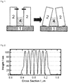
- Fig. 1 is of exemplary nature, the depicted spatial and dimensional relationships are not to be construed as an exact replica of the practical conditions.
- Silicon wafers were provided with 100 nm thick layers of an immersion photoresist.
- the photoresist layers were exposed to UV radiation of a wavelength of 193 through a mask using ultrapure water as the immersion liquid. Thereafter, the exposed photoresist layers were baked and developed with an aqueous developer solution containing tetramethylammonium hydroxide (TMAH).
- TMAH tetramethylammonium hydroxide
- the baked and developed photoresist layers were subjected to a chemical rinse treatment using a chemical rinse solution containing 0.002% by weight of surfactant (A1).
- the chemical rinse solution was applied on the wafer as a puddle. Thereafter, the silicon wafers were spun dry.
- Fig. 2 shows the respective height profile measured by AFM after the rinse treatment by using gemini surfactant A1.
- the dried patterned photoresist layers having patterns with line-space dimensions of 40 nm and an aspect ratio of about 2.5 did not show any pattern collapse.
- Example 1 was repeated except that gemini surfactant A2 was used instead of gemini surfactant A1 in the chemical rinse solution.
- Fig. 3 shows the respective height profile measured by AFM after the rinse treatment by using gemini surfactant A2.
- the dried patterned photoresist layers having photoresist line-width dimensions of 40 nm and an aspect ratio of about 2.5 did not show any pattern collapse.
- Example 1 was repeated except that ultra pure water without any additive was used in the chemical rinse solution.
- Fig. 4 shows the result of a photoresist development treatment by using ultra pure water without any additive.
- the dried patterned photoresist layers having photoresist line-width dimensions of 40 nm and an aspect ratio of about 2.5 showed significantly increased pattern collapse compared to the rinse according to examples 1 and 2.
Landscapes
- Chemical & Material Sciences (AREA)
- Physics & Mathematics (AREA)
- General Physics & Mathematics (AREA)
- Oil, Petroleum & Natural Gas (AREA)
- Life Sciences & Earth Sciences (AREA)
- Wood Science & Technology (AREA)
- Organic Chemistry (AREA)
- Chemical Kinetics & Catalysis (AREA)
- Engineering & Computer Science (AREA)
- Photosensitive Polymer And Photoresist Processing (AREA)
- Preparing Plates And Mask In Photomechanical Process (AREA)
- Exposure Of Semiconductors, Excluding Electron Or Ion Beam Exposure (AREA)
- Cleaning Or Drying Semiconductors (AREA)
- Materials For Photolithography (AREA)
- Exposure And Positioning Against Photoresist Photosensitive Materials (AREA)
- Detergent Compositions (AREA)
Claims (15)
- Utilisation d'un additif géminé représenté par la formule générale I dans des compositions aqueuses pour un rinçage de réduction de défauts de substrats en semi-conducteur après le développement de la résine photosensible ou de masques photolithographiques :
 X est un groupe divalent, pour chaque motif répété 1 à n indépendamment choisi entre(a) un groupe alcanediyle en C1 à C20 linéaire ou ramifié, qui peut éventuellement être substitué et qui peut éventuellement être interrompu par jusqu'à 5 hétéroatomes choisis entre O et N,(b) un groupe cycloalcanediyle en C5 à C20, qui peut éventuellement être substitué et qui peut éventuellement être interrompu par jusqu'à 5 hétéroatomes choisis entre O et N,(c) un groupe organique en C6 à C20 de formule -X1-A-X2-, dans lequel X1 et X2 sont indépendamment choisis parmi les groupes alcanediyle en C1 à C7 linéaires ou ramifiés et A est choisi entre une fraction aromatique en C5 à C12 ou un groupe cycloalcanediyle en C5 à C30, dont les atomes H peuvent éventuellement être remplacés et dont les atomes C peuvent éventuellement être interrompus par jusqu'à 5 hétéroatomes choisis entre O et N,(d) un radical divalent de polyoxyalkylène de formule II :
 R1 et R2 sont des groupes monovalents indépendamment choisis entre H, un groupe alkyle en C1 à C20 linéaire ou ramifié, cycloalkyle en C5 à C20, aryle en C5 à C20, alkylaryle en C6 à C20, arylalkyle en C6 à C20 ou hydroxyalkyle en C1 à C20 ou des homopolymères ou copolymères d'oxyalkylène en C2 à C4, tous pouvant éventuellement être en outre substitués ;R3 et R4 sont des groupes monovalents indépendamment choisis entre un groupe alkyle en C5 à C30 linéaire ou ramifié, un groupe cycloalkyle en C5 à C30, un groupe hydroxyalkyle en C1 à C20 et des homopolymères ou copolymères d'oxyalkylène en C2 à C4, tous pouvant éventuellement être substitués, et les R3-R4 par paires et R4-R4 et R3-R3 adjacents pouvant éventuellement former ensemble un groupe divalent X, et peuvent également être un prolongement Q de la molécule par ramification et, si n est supérieur ou égal à 2, R3, R4 ou R3 et R4 peuvent également être des atomes d'hydrogène ;n est un nombre entier de 1 à 5 ou, dans le cas où au moins l'un de X, R3 et R4 comprend un groupe polyoxyalkylène en C2 à C4, n peut être un nombre entier de 1 à 10000 et à condition que, si au moins un Q est présent, n comprenne tous les motifs répétés de ramifications Q ;Q est
 z est un nombre entier, qui est choisi pour que le tensioactif global ne soit pas électriquement chargé ;Z est un contre-ion.
 - Utilisation selon la revendication 1, dans laquelle X est choisi parmi les groupes alcanediyle en C3-C12 linéaires ou ramifiés non substitués.
- Utilisation selon la revendication 1, dans laquelle X est choisi parmi les groupes butane-1,6-diyle, hexane-1,6-diyle ou octane-1,8-diyle.
- Utilisation selon la revendication 1, dans laquelle X est choisi parmi les groupes de formule X3-O-X4, X3 et X4 étant des groupes alcanediyle en C1-C9 linéaires ou ramifiés.
- Utilisation selon la revendication 1, dans laquelle X1 et X2 sont indépendamment choisis parmi les groupes méthanediyle, éthanediyle, propanediyle et butanediyle et A est choisi entre le benzène et l'anthracène.
- Utilisation selon l'une quelconque des revendications précédentes, dans laquelle R1 et R2 sont indépendamment choisis parmi les groupes alcanediyle en C1-C12
- Utilisation selon l'une quelconque des revendications précédentes, dans laquelle R1 est choisi parmi H et R2 est indépendamment choisi entre H, un groupe alkyle en C1 à C20 linéaire ou ramifié, cycloalkyle en C5 à C20, aryle en C5 à C20, alkylaryle en C6 à C20, arylalkyle en C6 à C20 ou hydroxyalkyle en C1 à C20 ou des homopolymères ou copolymères d'oxyalkylène en C2 à C4, tous pouvant éventuellement être en outre substitués.
- Utilisation selon l'une quelconque des revendications précédentes, dans laquelle R3 et R4 sont choisis parmi les groupes de formule VI
 X3 est choisi entre une liaison chimique et un groupe alcanediyle en C1 à C4 linéaire ou ramifié, de préférence linéaire, de préférence par-dessus tout X3 est un groupe méthanediyle,R5 est choisi entre OH, H et un groupe alkyle en C1-C5 linéaire ou ramifié, de préférence R5 est un groupe méthyle ou OH,R6 est choisi entre H et un groupe alkyle en C1 à C20 linéaire ou ramifié, un groupe cycloalkyle en C1 à C20, un groupe aryle en C1 à C20, un groupe alkylaryle en C1 à C20 et un groupe arylalkyle en C1 à C20,R7 est choisi entre H et un groupe alkyle en C1 à C10 linéaire ou ramifié, de préférence R7 est un groupe méthyle ou tert-butyle.
 - Utilisation selon l'une quelconque des revendications 1 à 7, dans laquelle R3 et R4 sont choisis parmi les groupes de formule V
 u est un nombre entier de 0 à 100 ;R8 est, pour chaque motif répété u indépendamment, choisi entre H et un groupe alkyle en C1 à C2 linéaire ou ramifié etR10 est choisi parmi les groupes hydroxy (-OH), carboxy (-CO-OH ou ses sels), amine (-NH2), amide (-CO-NH2), sulfonamide (-SO2-NH2), sulfonate (-SO2OH ou ses sels), sulfate (-OSO2OH ou ses sels), phosphonate (-PO(OH)2 ou ses sels) et phosphate (-O-PO(OH)2 ou ses sels).
 - Utilisation selon l'une quelconque des revendications précédentes, dans laquelle le substrat comprend des structures comprenant des ouvertures inférieures ou égales à 30 nm.
- Procédé pour la fabrication de dispositifs à circuit intégré, de dispositifs optiques, de micromachines et de dispositifs mécaniques de précision, le procédé comprenant les étapes consistant à(a) fournir un substrat,(b) doter le substrat d'une couche de résine photosensible,(c) exposer la couche de résine photosensible à un rayonnement actinique à travers un masque avec ou sans un liquide d'immersion,(d) mettre en contact le substrat au moins une fois avec une composition de développement pour le développement de la résine photosensible pour obtenir un motif ayant une dimension des espaces entre les lignes inférieure ou égale à 32 nm et un rapport de forme > 2,(e) mettre en contact le substrat au moins une fois avec une composition aqueuse de nettoyage,dans lequel l'au moins une composition de nettoyage de l'étape (e) comprend un additif géminé de formule (I).
- Procédé selon la revendication 11, dans lequel les couches de matériau à motif ont des dimensions des espaces entre les lignes inférieures ou égales à 32 nm et des rapports de forme supérieurs à 10 pour les structures qui ne sont pas en résine photosensible et des rapports de forme supérieurs à 2 pour des structures en résine photosensible.
- Procédé selon l'une quelconque des revendications 11 à 12, dans lequel la composition contient, par rapport au poids total de la solution, 0, 0005 à 1 % en poids de l'additif géminé.
- Procédé selon l'une quelconque des revendications 11 à 13, dans lequel le substrat est fourni par un processus photolithographique comprenant les étapes consistant à(i) doter le substrat d'une résine photosensible par immersion, d'une résine photosensible par EUV ou d'une résine photosensible par faisceau d'électrons ;(ii) exposer la couche de résine photosensible à un rayonnement actinique à travers un masque avec ou sans un liquide d'immersion ;(iii)développer la couche de résine photosensible exposée avec une solution d'agent de développement pour obtenir un motif ayant des dimensions des espaces entre les lignes inférieures ou égales à 32 nm et un rapport de forme > 2 ;(iv) appliquer une solution de rinçage chimique à la couche de résine photosensible à motif développée ; et(v) sécher par centrifugation le substrat en semi-conducteur après l'application de la solution de rinçage chimique ;dans lequel au moins l'un des suivants . le liquide d'immersion et la solution de rinçage chimique, est une solution aqueuse comprenant un additif géminé.
- Procédé selon l'une quelconque des revendications 11 à 14, caractérisé en ce qu'il est utilisé pour la prévention de l'affaissement de motif, pour la réduction de la rugosité de bord de ligne, pour la prévention et l'élimination de défauts de type traces d'eau et pour la réduction de défauts par élimination de particules.
Priority Applications (1)
| Application Number | Priority Date | Filing Date | Title |
|---|---|---|---|
| EP17195200.5A EP3299891B1 (fr) | 2012-07-10 | 2013-07-01 | Utilisation de compositions comprenant des additifs géminés pour le traitement de substrats semiconducteurs. |
Applications Claiming Priority (2)
| Application Number | Priority Date | Filing Date | Title |
|---|---|---|---|
| US201261669686P | 2012-07-10 | 2012-07-10 | |
| PCT/IB2013/055392 WO2014009847A1 (fr) | 2012-07-10 | 2013-07-01 | Compositions pour traitement anti-affaissement de motif comprenant des additifs géminés |
Related Child Applications (1)
| Application Number | Title | Priority Date | Filing Date |
|---|---|---|---|
| EP17195200.5A Division EP3299891B1 (fr) | 2012-07-10 | 2013-07-01 | Utilisation de compositions comprenant des additifs géminés pour le traitement de substrats semiconducteurs. |
Publications (3)
| Publication Number | Publication Date |
|---|---|
| EP2872948A1 EP2872948A1 (fr) | 2015-05-20 |
| EP2872948A4 EP2872948A4 (fr) | 2016-11-02 |
| EP2872948B1 true EP2872948B1 (fr) | 2017-10-11 |
Family
ID=49915473
Family Applications (2)
| Application Number | Title | Priority Date | Filing Date |
|---|---|---|---|
| EP17195200.5A Active EP3299891B1 (fr) | 2012-07-10 | 2013-07-01 | Utilisation de compositions comprenant des additifs géminés pour le traitement de substrats semiconducteurs. |
| EP13816602.0A Not-in-force EP2872948B1 (fr) | 2012-07-10 | 2013-07-01 | Compositions pour traitement anti-affaissement de motif comprenant des additifs géminés |
Family Applications Before (1)
| Application Number | Title | Priority Date | Filing Date |
|---|---|---|---|
| EP17195200.5A Active EP3299891B1 (fr) | 2012-07-10 | 2013-07-01 | Utilisation de compositions comprenant des additifs géminés pour le traitement de substrats semiconducteurs. |
Country Status (11)
| Country | Link |
|---|---|
| US (1) | US10385295B2 (fr) |
| EP (2) | EP3299891B1 (fr) |
| JP (1) | JP6324955B2 (fr) |
| KR (1) | KR102107367B1 (fr) |
| CN (1) | CN104428716B (fr) |
| IL (1) | IL236408B (fr) |
| MY (1) | MY184912A (fr) |
| RU (1) | RU2015104112A (fr) |
| SG (1) | SG11201500098XA (fr) |
| TW (1) | TWI611274B (fr) |
| WO (1) | WO2014009847A1 (fr) |
Families Citing this family (7)
| Publication number | Priority date | Publication date | Assignee | Title |
|---|---|---|---|---|
| JP2015168680A (ja) * | 2014-03-11 | 2015-09-28 | 東ソー株式会社 | ジェミニ型界面活性剤 |
| JP6325464B2 (ja) * | 2015-01-05 | 2018-05-16 | 信越化学工業株式会社 | 現像液及びこれを用いたパターン形成方法 |
| JP2016139774A (ja) * | 2015-01-23 | 2016-08-04 | 富士フイルム株式会社 | パターン処理方法、半導体基板製品の製造方法およびパターン構造の前処理液 |
| KR102760295B1 (ko) * | 2017-11-28 | 2025-01-24 | 바스프 에스이 | 제품을 세정하거나 또는 헹구기 위한, 1 차 및 2 차 계면활성제를 포함하는 조성물 |
| JP7498544B2 (ja) * | 2018-05-08 | 2024-06-12 | 日本化薬株式会社 | 洗浄液及びインクジェットプリンタの洗浄方法 |
| US12518960B2 (en) * | 2020-07-09 | 2026-01-06 | Basf Se | Composition comprising a siloxane and an alkane for avoiding pattern collapse when treating patterned materials with line-space dimensions of 50 NM or below |
| JP7802644B2 (ja) * | 2021-11-09 | 2026-01-20 | 信越化学工業株式会社 | 半導体基板パターン倒壊抑制用充填膜形成材料及び半導体基板の処理方法 |
Family Cites Families (20)
| Publication number | Priority date | Publication date | Assignee | Title |
|---|---|---|---|---|
| JP4027494B2 (ja) * | 1998-04-07 | 2007-12-26 | 花王株式会社 | リンス剤組成物 |
| US7129199B2 (en) * | 2002-08-12 | 2006-10-31 | Air Products And Chemicals, Inc. | Process solutions containing surfactants |
| TW558736B (en) | 2000-02-26 | 2003-10-21 | Shipley Co Llc | Method of reducing defects |
| US20050164903A1 (en) * | 2001-08-03 | 2005-07-28 | Ki-Hwan Ko | Complexed surfactant system |
| KR20030012692A (ko) * | 2001-08-03 | 2003-02-12 | 주식회사 엘지생활건강 | 계면활성제 시스템 |
| US6641986B1 (en) | 2002-08-12 | 2003-11-04 | Air Products And Chemicals, Inc. | Acetylenic diol surfactant solutions and methods of using same |
| US7700257B2 (en) * | 2003-03-28 | 2010-04-20 | Tokyo Ohka Kogyo Co., Ltd. | Photoresist composition and resist pattern formation method by the use thereof |
| US20040259371A1 (en) * | 2003-06-18 | 2004-12-23 | Zhijian Lu | Reduction of resist defects |
| US20050158672A1 (en) | 2003-12-22 | 2005-07-21 | Matsushita Electric Industrial Co., Ltd. | Pattern formation method |
| KR100574349B1 (ko) * | 2004-02-03 | 2006-04-27 | 삼성전자주식회사 | 세정액 조성물 및 이를 이용한 반도체 장치의 세정방법 |
| US20080299487A1 (en) | 2007-05-31 | 2008-12-04 | Taiwan Semiconductor Manufacturing Company, Ltd. | Lithography material and lithography process |
| CN101236357B (zh) * | 2007-01-30 | 2012-07-04 | 住友化学株式会社 | 化学放大型抗蚀剂组合物 |
| US20080280230A1 (en) | 2007-05-10 | 2008-11-13 | Taiwan Semiconductor Manufacturing Company, Ltd. | Photolithography process including a chemical rinse |
| JP2009237169A (ja) * | 2008-03-26 | 2009-10-15 | Fujifilm Corp | 平版印刷版の作製方法 |
| JP2009237168A (ja) * | 2008-03-26 | 2009-10-15 | Fujifilm Corp | 平版印刷版の作製方法 |
| CN101766973B (zh) * | 2009-01-07 | 2012-06-13 | 湖北大学 | 一种对称型阳离子表面活性剂及其制备方法 |
| JP5624753B2 (ja) | 2009-03-31 | 2014-11-12 | 東京応化工業株式会社 | リソグラフィー用洗浄液及びこれを用いたレジストパターンの形成方法 |
| MY161218A (en) | 2011-01-25 | 2017-04-14 | Basf Se | Use of surfactants having at least three short-chain perfluorinated groups rf for manufacturing integrated circuits having patterns with line-space dimensions below 50nm |
| RU2585322C2 (ru) | 2011-03-18 | 2016-05-27 | Басф Се | Способ получения интегральных схем, оптических устройств, микромашин и механических высокоточных устройств, имеющих слои структурированного материала со строчным интервалом 50 нм и менее |
| SG11201504607QA (en) * | 2012-12-14 | 2015-07-30 | Basf Se | Use of compositions comprising a surfactant and a hydrophobizer for avoiding anti pattern collapse when treating patterned materials with line-space dimensions of 50 nm or below |
-
2013
- 2013-07-01 SG SG11201500098XA patent/SG11201500098XA/en unknown
- 2013-07-01 CN CN201380035822.7A patent/CN104428716B/zh active Active
- 2013-07-01 WO PCT/IB2013/055392 patent/WO2014009847A1/fr not_active Ceased
- 2013-07-01 US US14/412,737 patent/US10385295B2/en active Active
- 2013-07-01 EP EP17195200.5A patent/EP3299891B1/fr active Active
- 2013-07-01 KR KR1020157003355A patent/KR102107367B1/ko active Active
- 2013-07-01 JP JP2015521102A patent/JP6324955B2/ja active Active
- 2013-07-01 RU RU2015104112A patent/RU2015104112A/ru not_active Application Discontinuation
- 2013-07-01 MY MYPI2015000032A patent/MY184912A/en unknown
- 2013-07-01 EP EP13816602.0A patent/EP2872948B1/fr not_active Not-in-force
- 2013-07-08 TW TW102124316A patent/TWI611274B/zh active
-
2014
- 2014-12-23 IL IL236408A patent/IL236408B/en active IP Right Grant
Non-Patent Citations (1)
| Title |
|---|
| None * |
Also Published As
| Publication number | Publication date |
|---|---|
| EP2872948A1 (fr) | 2015-05-20 |
| RU2015104112A (ru) | 2016-08-27 |
| CN104428716A (zh) | 2015-03-18 |
| MY184912A (en) | 2021-04-30 |
| IL236408A0 (en) | 2015-02-26 |
| TW201418910A (zh) | 2014-05-16 |
| EP3299891A1 (fr) | 2018-03-28 |
| WO2014009847A1 (fr) | 2014-01-16 |
| US10385295B2 (en) | 2019-08-20 |
| JP6324955B2 (ja) | 2018-05-16 |
| EP3299891B1 (fr) | 2019-05-15 |
| IL236408B (en) | 2020-03-31 |
| KR102107367B1 (ko) | 2020-05-07 |
| US20150159123A1 (en) | 2015-06-11 |
| JP2015529840A (ja) | 2015-10-08 |
| KR20150036461A (ko) | 2015-04-07 |
| EP2872948A4 (fr) | 2016-11-02 |
| TWI611274B (zh) | 2018-01-11 |
| CN104428716B (zh) | 2019-06-14 |
| SG11201500098XA (en) | 2015-02-27 |
Similar Documents
| Publication | Publication Date | Title |
|---|---|---|
| EP2872948B1 (fr) | Compositions pour traitement anti-affaissement de motif comprenant des additifs géminés | |
| US9557652B2 (en) | Use of compositions comprising a surfactant and a hydrophobizer for avoiding anti pattern collapse when treating patterned materials with line-space dimensions of 50 nm or below | |
| US9184057B2 (en) | Method for manufacturing integrated circuit devices, optical devices, micromachines and mechanical precision devices having patterned material layers with line-space dimensions of 50 nm and less | |
| TWI772552B (zh) | 含矽氧烷型添加劑之組成物用於在處理具有50nm或低於50nm之線性空間尺寸之圖案材料時避免圖案塌陷之用途 | |
| US12146125B2 (en) | Use of compositions comprising a solvent mixture for avoiding pattern collapse when treating patterned materials with line-space dimensions of 50 nm or below | |
| KR102107370B1 (ko) | 집적 회로 기기, 광학 기기, 초소형 기계 장비 및 정밀 기계 장비 제조용 조성물 | |
| EP2500777A1 (fr) | Procédé de fabrication de dispositifs de circuit intégré, dispositifs optiques, micromachines et de dispositifs de précision mécanique dotés de couches de matériau avec des motifs de dimensions inférieures ou égales à 50 nm |
Legal Events
| Date | Code | Title | Description |
|---|---|---|---|
| PUAI | Public reference made under article 153(3) epc to a published international application that has entered the european phase |
Free format text: ORIGINAL CODE: 0009012 |
|
| 17P | Request for examination filed |
Effective date: 20150210 |
|
| AK | Designated contracting states |
Kind code of ref document: A1 Designated state(s): AL AT BE BG CH CY CZ DE DK EE ES FI FR GB GR HR HU IE IS IT LI LT LU LV MC MK MT NL NO PL PT RO RS SE SI SK SM TR |
|
| AX | Request for extension of the european patent |
Extension state: BA ME |
|
| DAX | Request for extension of the european patent (deleted) | ||
| REG | Reference to a national code |
Ref country code: DE Ref legal event code: R079 Ref document number: 602013027898 Country of ref document: DE Free format text: PREVIOUS MAIN CLASS: G03F0007320000 Ipc: G03F0007400000 |
|
| RA4 | Supplementary search report drawn up and despatched (corrected) |
Effective date: 20160929 |
|
| RIC1 | Information provided on ipc code assigned before grant |
Ipc: G03F 7/40 20060101AFI20160923BHEP Ipc: C11D 1/40 20060101ALI20160923BHEP |
|
| GRAP | Despatch of communication of intention to grant a patent |
Free format text: ORIGINAL CODE: EPIDOSNIGR1 |
|
| INTG | Intention to grant announced |
Effective date: 20170531 |
|
| GRAS | Grant fee paid |
Free format text: ORIGINAL CODE: EPIDOSNIGR3 |
|
| GRAA | (expected) grant |
Free format text: ORIGINAL CODE: 0009210 |
|
| AK | Designated contracting states |
Kind code of ref document: B1 Designated state(s): AL AT BE BG CH CY CZ DE DK EE ES FI FR GB GR HR HU IE IS IT LI LT LU LV MC MK MT NL NO PL PT RO RS SE SI SK SM TR |
|
| REG | Reference to a national code |
Ref country code: GB Ref legal event code: FG4D |
|
| REG | Reference to a national code |
Ref country code: CH Ref legal event code: EP |
|
| REG | Reference to a national code |
Ref country code: IE Ref legal event code: FG4D |
|
| REG | Reference to a national code |
Ref country code: AT Ref legal event code: REF Ref document number: 936574 Country of ref document: AT Kind code of ref document: T Effective date: 20171115 |
|
| REG | Reference to a national code |
Ref country code: DE Ref legal event code: R096 Ref document number: 602013027898 Country of ref document: DE |
|
| REG | Reference to a national code |
Ref country code: NL Ref legal event code: FP |
|
| REG | Reference to a national code |
Ref country code: LT Ref legal event code: MG4D |
|
| REG | Reference to a national code |
Ref country code: AT Ref legal event code: MK05 Ref document number: 936574 Country of ref document: AT Kind code of ref document: T Effective date: 20171011 |
|
| PG25 | Lapsed in a contracting state [announced via postgrant information from national office to epo] |
Ref country code: ES Free format text: LAPSE BECAUSE OF FAILURE TO SUBMIT A TRANSLATION OF THE DESCRIPTION OR TO PAY THE FEE WITHIN THE PRESCRIBED TIME-LIMIT Effective date: 20171011 Ref country code: LT Free format text: LAPSE BECAUSE OF FAILURE TO SUBMIT A TRANSLATION OF THE DESCRIPTION OR TO PAY THE FEE WITHIN THE PRESCRIBED TIME-LIMIT Effective date: 20171011 Ref country code: FI Free format text: LAPSE BECAUSE OF FAILURE TO SUBMIT A TRANSLATION OF THE DESCRIPTION OR TO PAY THE FEE WITHIN THE PRESCRIBED TIME-LIMIT Effective date: 20171011 Ref country code: SE Free format text: LAPSE BECAUSE OF FAILURE TO SUBMIT A TRANSLATION OF THE DESCRIPTION OR TO PAY THE FEE WITHIN THE PRESCRIBED TIME-LIMIT Effective date: 20171011 Ref country code: NO Free format text: LAPSE BECAUSE OF FAILURE TO SUBMIT A TRANSLATION OF THE DESCRIPTION OR TO PAY THE FEE WITHIN THE PRESCRIBED TIME-LIMIT Effective date: 20180111 |
|
| PG25 | Lapsed in a contracting state [announced via postgrant information from national office to epo] |
Ref country code: LV Free format text: LAPSE BECAUSE OF FAILURE TO SUBMIT A TRANSLATION OF THE DESCRIPTION OR TO PAY THE FEE WITHIN THE PRESCRIBED TIME-LIMIT Effective date: 20171011 Ref country code: GR Free format text: LAPSE BECAUSE OF FAILURE TO SUBMIT A TRANSLATION OF THE DESCRIPTION OR TO PAY THE FEE WITHIN THE PRESCRIBED TIME-LIMIT Effective date: 20180112 Ref country code: RS Free format text: LAPSE BECAUSE OF FAILURE TO SUBMIT A TRANSLATION OF THE DESCRIPTION OR TO PAY THE FEE WITHIN THE PRESCRIBED TIME-LIMIT Effective date: 20171011 Ref country code: HR Free format text: LAPSE BECAUSE OF FAILURE TO SUBMIT A TRANSLATION OF THE DESCRIPTION OR TO PAY THE FEE WITHIN THE PRESCRIBED TIME-LIMIT Effective date: 20171011 Ref country code: AT Free format text: LAPSE BECAUSE OF FAILURE TO SUBMIT A TRANSLATION OF THE DESCRIPTION OR TO PAY THE FEE WITHIN THE PRESCRIBED TIME-LIMIT Effective date: 20171011 Ref country code: BG Free format text: LAPSE BECAUSE OF FAILURE TO SUBMIT A TRANSLATION OF THE DESCRIPTION OR TO PAY THE FEE WITHIN THE PRESCRIBED TIME-LIMIT Effective date: 20180111 Ref country code: IS Free format text: LAPSE BECAUSE OF FAILURE TO SUBMIT A TRANSLATION OF THE DESCRIPTION OR TO PAY THE FEE WITHIN THE PRESCRIBED TIME-LIMIT Effective date: 20180211 |
|
| REG | Reference to a national code |
Ref country code: DE Ref legal event code: R097 Ref document number: 602013027898 Country of ref document: DE |
|
| REG | Reference to a national code |
Ref country code: FR Ref legal event code: PLFP Year of fee payment: 6 |
|
| PG25 | Lapsed in a contracting state [announced via postgrant information from national office to epo] |
Ref country code: EE Free format text: LAPSE BECAUSE OF FAILURE TO SUBMIT A TRANSLATION OF THE DESCRIPTION OR TO PAY THE FEE WITHIN THE PRESCRIBED TIME-LIMIT Effective date: 20171011 Ref country code: CZ Free format text: LAPSE BECAUSE OF FAILURE TO SUBMIT A TRANSLATION OF THE DESCRIPTION OR TO PAY THE FEE WITHIN THE PRESCRIBED TIME-LIMIT Effective date: 20171011 Ref country code: SK Free format text: LAPSE BECAUSE OF FAILURE TO SUBMIT A TRANSLATION OF THE DESCRIPTION OR TO PAY THE FEE WITHIN THE PRESCRIBED TIME-LIMIT Effective date: 20171011 Ref country code: DK Free format text: LAPSE BECAUSE OF FAILURE TO SUBMIT A TRANSLATION OF THE DESCRIPTION OR TO PAY THE FEE WITHIN THE PRESCRIBED TIME-LIMIT Effective date: 20171011 |
|
| PLBE | No opposition filed within time limit |
Free format text: ORIGINAL CODE: 0009261 |
|
| STAA | Information on the status of an ep patent application or granted ep patent |
Free format text: STATUS: NO OPPOSITION FILED WITHIN TIME LIMIT |
|
| PG25 | Lapsed in a contracting state [announced via postgrant information from national office to epo] |
Ref country code: PL Free format text: LAPSE BECAUSE OF FAILURE TO SUBMIT A TRANSLATION OF THE DESCRIPTION OR TO PAY THE FEE WITHIN THE PRESCRIBED TIME-LIMIT Effective date: 20171011 Ref country code: RO Free format text: LAPSE BECAUSE OF FAILURE TO SUBMIT A TRANSLATION OF THE DESCRIPTION OR TO PAY THE FEE WITHIN THE PRESCRIBED TIME-LIMIT Effective date: 20171011 Ref country code: SM Free format text: LAPSE BECAUSE OF FAILURE TO SUBMIT A TRANSLATION OF THE DESCRIPTION OR TO PAY THE FEE WITHIN THE PRESCRIBED TIME-LIMIT Effective date: 20171011 |
|
| 26N | No opposition filed |
Effective date: 20180712 |
|
| PGFP | Annual fee paid to national office [announced via postgrant information from national office to epo] |
Ref country code: CY Payment date: 20180420 Year of fee payment: 14 |
|
| PG25 | Lapsed in a contracting state [announced via postgrant information from national office to epo] |
Ref country code: SI Free format text: LAPSE BECAUSE OF FAILURE TO SUBMIT A TRANSLATION OF THE DESCRIPTION OR TO PAY THE FEE WITHIN THE PRESCRIBED TIME-LIMIT Effective date: 20171011 |
|
| REG | Reference to a national code |
Ref country code: CH Ref legal event code: PL |
|
| PG25 | Lapsed in a contracting state [announced via postgrant information from national office to epo] |
Ref country code: MC Free format text: LAPSE BECAUSE OF FAILURE TO SUBMIT A TRANSLATION OF THE DESCRIPTION OR TO PAY THE FEE WITHIN THE PRESCRIBED TIME-LIMIT Effective date: 20171011 Ref country code: LU Free format text: LAPSE BECAUSE OF NON-PAYMENT OF DUE FEES Effective date: 20180701 |
|
| REG | Reference to a national code |
Ref country code: BE Ref legal event code: MM Effective date: 20180731 |
|
| PG25 | Lapsed in a contracting state [announced via postgrant information from national office to epo] |
Ref country code: LI Free format text: LAPSE BECAUSE OF NON-PAYMENT OF DUE FEES Effective date: 20180731 Ref country code: CH Free format text: LAPSE BECAUSE OF NON-PAYMENT OF DUE FEES Effective date: 20180731 |
|
| PG25 | Lapsed in a contracting state [announced via postgrant information from national office to epo] |
Ref country code: BE Free format text: LAPSE BECAUSE OF NON-PAYMENT OF DUE FEES Effective date: 20180731 |
|
| PG25 | Lapsed in a contracting state [announced via postgrant information from national office to epo] |
Ref country code: MT Free format text: LAPSE BECAUSE OF NON-PAYMENT OF DUE FEES Effective date: 20180701 |
|
| PG25 | Lapsed in a contracting state [announced via postgrant information from national office to epo] |
Ref country code: TR Free format text: LAPSE BECAUSE OF FAILURE TO SUBMIT A TRANSLATION OF THE DESCRIPTION OR TO PAY THE FEE WITHIN THE PRESCRIBED TIME-LIMIT Effective date: 20171011 |
|
| PG25 | Lapsed in a contracting state [announced via postgrant information from national office to epo] |
Ref country code: NL Free format text: LAPSE BECAUSE OF NON-PAYMENT OF DUE FEES Effective date: 20190801 |
|
| REG | Reference to a national code |
Ref country code: NL Ref legal event code: MM Effective date: 20190801 |
|
| PG25 | Lapsed in a contracting state [announced via postgrant information from national office to epo] |
Ref country code: HU Free format text: LAPSE BECAUSE OF FAILURE TO SUBMIT A TRANSLATION OF THE DESCRIPTION OR TO PAY THE FEE WITHIN THE PRESCRIBED TIME-LIMIT; INVALID AB INITIO Effective date: 20130701 Ref country code: PT Free format text: LAPSE BECAUSE OF FAILURE TO SUBMIT A TRANSLATION OF THE DESCRIPTION OR TO PAY THE FEE WITHIN THE PRESCRIBED TIME-LIMIT Effective date: 20171011 |
|
| PG25 | Lapsed in a contracting state [announced via postgrant information from national office to epo] |
Ref country code: MK Free format text: LAPSE BECAUSE OF NON-PAYMENT OF DUE FEES Effective date: 20171011 Ref country code: CY Free format text: LAPSE BECAUSE OF FAILURE TO SUBMIT A TRANSLATION OF THE DESCRIPTION OR TO PAY THE FEE WITHIN THE PRESCRIBED TIME-LIMIT Effective date: 20171011 |
|
| PG25 | Lapsed in a contracting state [announced via postgrant information from national office to epo] |
Ref country code: AL Free format text: LAPSE BECAUSE OF FAILURE TO SUBMIT A TRANSLATION OF THE DESCRIPTION OR TO PAY THE FEE WITHIN THE PRESCRIBED TIME-LIMIT Effective date: 20171011 |
|
| PGFP | Annual fee paid to national office [announced via postgrant information from national office to epo] |
Ref country code: IE Payment date: 20200721 Year of fee payment: 8 Ref country code: GB Payment date: 20200724 Year of fee payment: 8 |
|
| PGFP | Annual fee paid to national office [announced via postgrant information from national office to epo] |
Ref country code: IT Payment date: 20200721 Year of fee payment: 8 |
|
| GBPC | Gb: european patent ceased through non-payment of renewal fee |
Effective date: 20210701 |
|
| PG25 | Lapsed in a contracting state [announced via postgrant information from national office to epo] |
Ref country code: GB Free format text: LAPSE BECAUSE OF NON-PAYMENT OF DUE FEES Effective date: 20210701 |
|
| PG25 | Lapsed in a contracting state [announced via postgrant information from national office to epo] |
Ref country code: IT Free format text: LAPSE BECAUSE OF NON-PAYMENT OF DUE FEES Effective date: 20210701 Ref country code: IE Free format text: LAPSE BECAUSE OF NON-PAYMENT OF DUE FEES Effective date: 20210701 |
|
| PGFP | Annual fee paid to national office [announced via postgrant information from national office to epo] |
Ref country code: DE Payment date: 20240730 Year of fee payment: 12 |
|
| PGFP | Annual fee paid to national office [announced via postgrant information from national office to epo] |
Ref country code: FR Payment date: 20240725 Year of fee payment: 12 |
|
| REG | Reference to a national code |
Ref country code: DE Ref legal event code: R119 Ref document number: 602013027898 Country of ref document: DE |
|
| PG25 | Lapsed in a contracting state [announced via postgrant information from national office to epo] |
Ref country code: DE Free format text: LAPSE BECAUSE OF NON-PAYMENT OF DUE FEES Effective date: 20260203 |
|
| PG25 | Lapsed in a contracting state [announced via postgrant information from national office to epo] |
Ref country code: FR Free format text: LAPSE BECAUSE OF NON-PAYMENT OF DUE FEES Effective date: 20250731 |