EP2873079B1 - Couche magnétique modifiée ayant une anisotropie perpendiculaire améliorée utilisant des agents vitrifiants pour des applications spintroniques - Google Patents
Couche magnétique modifiée ayant une anisotropie perpendiculaire améliorée utilisant des agents vitrifiants pour des applications spintroniques Download PDFInfo
- Publication number
- EP2873079B1 EP2873079B1 EP13740162.6A EP13740162A EP2873079B1 EP 2873079 B1 EP2873079 B1 EP 2873079B1 EP 13740162 A EP13740162 A EP 13740162A EP 2873079 B1 EP2873079 B1 EP 2873079B1
- Authority
- EP
- European Patent Office
- Prior art keywords
- layer
- concentration
- free
- free layer
- tunnel barrier
- Prior art date
- Legal status (The legal status is an assumption and is not a legal conclusion. Google has not performed a legal analysis and makes no representation as to the accuracy of the status listed.)
- Active
Links
Images



Classifications
-
- H—ELECTRICITY
- H01—ELECTRIC ELEMENTS
- H01F—MAGNETS; INDUCTANCES; TRANSFORMERS; SELECTION OF MATERIALS FOR THEIR MAGNETIC PROPERTIES
- H01F10/00—Thin magnetic films, e.g. of one-domain structure
- H01F10/32—Spin-exchange-coupled multilayers, e.g. nanostructured superlattices
- H01F10/324—Exchange coupling of magnetic film pairs via a very thin non-magnetic spacer, e.g. by exchange with conduction electrons of the spacer
- H01F10/3254—Exchange coupling of magnetic film pairs via a very thin non-magnetic spacer, e.g. by exchange with conduction electrons of the spacer the spacer being semiconducting or insulating, e.g. for spin tunnel junction [STJ]
-
- G—PHYSICS
- G11—INFORMATION STORAGE
- G11C—STATIC STORES
- G11C11/00—Digital stores characterised by the use of particular electric or magnetic storage elements; Storage elements therefor
- G11C11/02—Digital stores characterised by the use of particular electric or magnetic storage elements; Storage elements therefor using magnetic elements
- G11C11/16—Digital stores characterised by the use of particular electric or magnetic storage elements; Storage elements therefor using magnetic elements using elements in which the storage effect is based on magnetic spin effect
- G11C11/161—Digital stores characterised by the use of particular electric or magnetic storage elements; Storage elements therefor using magnetic elements using elements in which the storage effect is based on magnetic spin effect details concerning the memory cell structure, e.g. the layers of the ferromagnetic memory cell
-
- H—ELECTRICITY
- H01—ELECTRIC ELEMENTS
- H01F—MAGNETS; INDUCTANCES; TRANSFORMERS; SELECTION OF MATERIALS FOR THEIR MAGNETIC PROPERTIES
- H01F10/00—Thin magnetic films, e.g. of one-domain structure
- H01F10/32—Spin-exchange-coupled multilayers, e.g. nanostructured superlattices
- H01F10/324—Exchange coupling of magnetic film pairs via a very thin non-magnetic spacer, e.g. by exchange with conduction electrons of the spacer
- H01F10/3286—Spin-exchange coupled multilayers having at least one layer with perpendicular magnetic anisotropy
-
- H—ELECTRICITY
- H01—ELECTRIC ELEMENTS
- H01F—MAGNETS; INDUCTANCES; TRANSFORMERS; SELECTION OF MATERIALS FOR THEIR MAGNETIC PROPERTIES
- H01F41/00—Apparatus or processes specially adapted for manufacturing or assembling magnets, inductances or transformers; Apparatus or processes specially adapted for manufacturing materials characterised by their magnetic properties
- H01F41/14—Apparatus or processes specially adapted for manufacturing or assembling magnets, inductances or transformers; Apparatus or processes specially adapted for manufacturing materials characterised by their magnetic properties for applying magnetic films to substrates
- H01F41/30—Apparatus or processes specially adapted for manufacturing or assembling magnets, inductances or transformers; Apparatus or processes specially adapted for manufacturing materials characterised by their magnetic properties for applying magnetic films to substrates for applying nanostructures, e.g. by molecular beam epitaxy [MBE]
- H01F41/302—Apparatus or processes specially adapted for manufacturing or assembling magnets, inductances or transformers; Apparatus or processes specially adapted for manufacturing materials characterised by their magnetic properties for applying magnetic films to substrates for applying nanostructures, e.g. by molecular beam epitaxy [MBE] for applying spin-exchange-coupled multilayers, e.g. nanostructured superlattices
- H01F41/305—Apparatus or processes specially adapted for manufacturing or assembling magnets, inductances or transformers; Apparatus or processes specially adapted for manufacturing materials characterised by their magnetic properties for applying magnetic films to substrates for applying nanostructures, e.g. by molecular beam epitaxy [MBE] for applying spin-exchange-coupled multilayers, e.g. nanostructured superlattices applying the spacer or adjusting its interface, e.g. in order to enable particular effect different from exchange coupling
- H01F41/307—Apparatus or processes specially adapted for manufacturing or assembling magnets, inductances or transformers; Apparatus or processes specially adapted for manufacturing materials characterised by their magnetic properties for applying magnetic films to substrates for applying nanostructures, e.g. by molecular beam epitaxy [MBE] for applying spin-exchange-coupled multilayers, e.g. nanostructured superlattices applying the spacer or adjusting its interface, e.g. in order to enable particular effect different from exchange coupling insulating or semiconductive spacer
-
- H—ELECTRICITY
- H10—SEMICONDUCTOR DEVICES; ELECTRIC SOLID-STATE DEVICES NOT OTHERWISE PROVIDED FOR
- H10N—ELECTRIC SOLID-STATE DEVICES NOT OTHERWISE PROVIDED FOR
- H10N50/00—Galvanomagnetic devices
- H10N50/10—Magnetoresistive devices
-
- H—ELECTRICITY
- H10—SEMICONDUCTOR DEVICES; ELECTRIC SOLID-STATE DEVICES NOT OTHERWISE PROVIDED FOR
- H10N—ELECTRIC SOLID-STATE DEVICES NOT OTHERWISE PROVIDED FOR
- H10N50/00—Galvanomagnetic devices
- H10N50/80—Constructional details
- H10N50/85—Materials of the active region
-
- B—PERFORMING OPERATIONS; TRANSPORTING
- B82—NANOTECHNOLOGY
- B82Y—SPECIFIC USES OR APPLICATIONS OF NANOSTRUCTURES; MEASUREMENT OR ANALYSIS OF NANOSTRUCTURES; MANUFACTURE OR TREATMENT OF NANOSTRUCTURES
- B82Y25/00—Nanomagnetism, e.g. magnetoimpedance, anisotropic magnetoresistance, giant magnetoresistance or tunneling magnetoresistance
-
- H—ELECTRICITY
- H01—ELECTRIC ELEMENTS
- H01F—MAGNETS; INDUCTANCES; TRANSFORMERS; SELECTION OF MATERIALS FOR THEIR MAGNETIC PROPERTIES
- H01F10/00—Thin magnetic films, e.g. of one-domain structure
- H01F10/32—Spin-exchange-coupled multilayers, e.g. nanostructured superlattices
- H01F10/324—Exchange coupling of magnetic film pairs via a very thin non-magnetic spacer, e.g. by exchange with conduction electrons of the spacer
- H01F10/3254—Exchange coupling of magnetic film pairs via a very thin non-magnetic spacer, e.g. by exchange with conduction electrons of the spacer the spacer being semiconducting or insulating, e.g. for spin tunnel junction [STJ]
- H01F10/3259—Spin-exchange-coupled multilayers comprising at least a nanooxide layer [NOL], e.g. with a NOL spacer
Definitions
- the present disclosure relates to a magnetic tunnel junction element comprised of at least one ferromagnetic layer or multilayer exhibiting perpendicular magnetic anisotropy (PMA) wherein the ferromagnetic layer is doped with a glassing agent to retain an amorphous character in a center region thereof and thereby reduce crystalline anisotropy and provide a higher PMA for a given magnetic moment along with higher thermal stability for the device.
- PMA perpendicular magnetic anisotropy
- Magnetoresistive Random Access Memory based on the integration of silicon CMOS with magnetic tunnel junction (MTJ) technology, is a major emerging technology that is highly competitive with existing semiconductor memories such as SRAM, DRAM, and Flash.
- spin-transfer (spin torque) magnetization switching described by C. Slonczewski in "Current driven excitation of magnetic multilayers", J. Magn. Magn. Mater. V 159, L1-L7 (1996 ), has recently stimulated considerable interest due to its potential application for spintronic devices such as STT-MRAM on a gigabit scale.
- Both field-MRAM and STT-MRAM have a MTJ element based on a tunneling magneto-resistance (TMR) effect wherein a stack of layers has a configuration in which two ferromagnetic layers are separated by a thin non-magnetic dielectric layer.
- TMR tunneling magneto-resistance
- One of the ferromagnetic layers has a magnetic moment that is pinned in a first direction while the other ferromagnetic layer has a magnetic moment which is free to rotate in a direction that is either parallel or anti-parallel to the first direction.
- the use of external magnetic fields generated by current carrying lines to switch the magnetic moment direction of the free layer becomes problematic.
- spin transfer (spin torque) device One of the keys to manufacturability of ultra-high density MRAMs is to provide a robust magnetic switching margin by eliminating the half-select disturb issue. For this reason, a new type of device called a spin transfer (spin torque) device was developed. Compared with conventional MRAM, spin-transfer torque or STT-MRAM has an advantage in avoiding the half select problem and writing disturbance between adjacent cells. The spin-transfer effect arises from the spin dependent electron transport properties of ferromagnetic-spacer-ferromagnetic multilayers.
- spin-polarized current When a spin-polarized current transverses a magnetic multilayer in a current perpendicular to plane (CPP) configuration, the spin angular moment of electrons incident on a ferromagnetic layer interacts with magnetic moments of the ferromagnetic layer near the interface between the ferromagnetic layer and non-magnetic spacer. Through this interaction, the electrons transfer a portion of their angular momentum to the ferromagnetic free layer. As a result, spin-polarized current can switch the magnetization direction of the ferromagnetic free layer if the current density is sufficiently high, and if the dimensions of the multilayer are small.
- CPP current perpendicular to plane
- the ultra-small MTJs (also referred to as nanomagnets) must exhibit a magnetoresistive (MR) ratio that is much higher than in a conventional MRAM-MTJ which uses a NiFe free layer and AlOx as the tunnel barrier layer.
- MR magnetoresistive
- Jc critical current density
- a critical current for spin transfer switching which is defined as [(Ic + + Ic - ) /2], for the present 180 nm node sub-micron MTJ having a top-down oval shaped area of about 0.2 x 0.4 micron, is generally a few milliamperes.
- the critical current density (Jc), for example (Ic/A), is on the order of several 10 7 A/cm 2 . This high current density, which is required to induce the spin-transfer effect, could destroy a thin tunnel barrier made of AlOx, MgO, or the like.
- Ic and its Jc
- a preferred implementation is to employ a magnetic tunnel junction (MTJ) with a pinned ferromagnetic layer and free ferromagnetic layer separated by a tunneling oxide layer in a TMR configuration.
- MTJ magnetic tunnel junction
- this scheme has been widely studied, further improvements in overall performance are needed before a domain wall motion device is used commercially as a memory element in MRAM or as a sensor in hard disk drive (HDD) heads.
- the two magnetic layers in a TMR configuration can either have their magnetization pointing in the plane or out of the plane of the film.
- An example of in-plane magnetization is shown on side (a) of FIG. 1 where a pinned layer 10 has a magnetic moment along an x-axis and the free layer 12 has a magnetic moment free to rotate in a (+) or (-) x-axis direction.
- An insulating (tunnel barrier) layer 11 separates the aforementioned two ferromagnetic layers.
- Out of plane magnetization (PMA) is depicted on side (b) of FIG.
- pinned layer 20 has a magnetization pointing in a y-axis direction or perpendicular to the film plane and the free layer 21 has a magnetic moment that is free to rotate either in a (+) or (-) y-axis direction.
- the free layer and pinned layer magnetizations are parallel or anti-parallel in a quiescent state.
- storage of the digital information as a "1" or "0" magnetic state is provided by the direction of magnetization in the free layer 12 (or 21 ).
- the spin polarized current must be as small as possible.
- H k eff , ⁇ ⁇ DM s + 2 K U ⁇ , s M s d + H k , ⁇
- D (approximately 4 ⁇ ) is the demagnetizing factor of the structure
- M s is the saturation magnetization
- d is the thickness of the magnetic element
- H k, ⁇ is the crystalline anisotropy field
- K U ⁇ , s is the surface perpendicular anisotropy of the top and bottom surfaces of the magnetic element.
- H k, ⁇ is the sum of the crystalline anisotropy of all the grains defining the region of interest.
- the perpendicular anisotropy field of a magnetic layer is dominated by the shape anisotropy field on which little control is available.
- lower magnetization saturation decreases shape anisotropy and the spin-polarized switching current but also decreases thermal stability which is not desirable. Therefore, an improved configuration for a magnetic element is needed that provides improved thermal stability for a free layer with perpendicular magnetic anisotropy.
- perpendicular magnetic anisotropy can be enhanced at first and second free layer interfaces with adjoining layers in a MTJ stack while selectively crystallizing portions of the free layer adjacent to these interfaces, and maintaining amorphous character (lower magnetic moment) in a middle portion of the free layer.
- US 2012/0068285 A1 relates to a magnetoresistive effect element including a first magnetic layer including perpendicular anisotropy to a film surface and an invariable magnetization direction, the first magnetic layer having a magnetic film including an element selected from a first group including Tb, Gd, and Dy and an element selected from a second group including Co and Fe, a second magnetic layer including perpendicular magnetic anisotropy to the film surface and a variable magnetization direction, and a nonmagnetic layer between the first magnetic layer and the second magnetic layer.
- the magnetic film includes amorphous phases and crystals whose particle sizes are 0.5 nm or more.
- US 2010/0096716 A1 relates to a spin-torque transfer memory random access memory (STTMRAM) element including a fixed layer formed on top of a substrate and a tunnel layer formed upon the fixed layer and a composite free layer formed upon the tunnel barrier layer and made of an iron platinum alloy with at least one of X or Y material, X being from a group consisting of: boron (B), phosphorous (P), carbon (C), and nitride (N) and Y being from a group consisting of: tantalum (Ta), titanium (Ti), niobium (Nb), zirconium (Zr), tungsten (W), silicon (Si), copper (Cu), silver (Ag), aluminum (Al), chromium (Cr), tin (Sn), lead (Pb), antimony (Sb), hafnium (Hf) and bismuth (Bi), molybdenum (Mo) or rhodium (Ru), the magnetization direction of each of the composite
- US 2011/0032644 A1 relates to a method and system for providing a magnetic element and a magnetic memory utilizing the magnetic element.
- the magnetic element is used in a magnetic device that includes a contact electrically coupled to the magnetic element.
- the method and system include providing pinned, nonmagnetic spacer, and free layers.
- the free layer has an out-of-plane demagnetization energy and a perpendicular magnetic anisotropy corresponding to a perpendicular anisotropy energy that is less than the out-of-plane demagnetization energy.
- the nonmagnetic spacer layer is between the pinned and free layers.
- the method and system also include providing a perpendicular capping layer adjoining the free layer and the contact. The perpendicular capping layer induces at least part of the perpendicular magnetic anisotropy in the free layer.
- the magnetic element is configured to allow the free layer to be switched between magnetic states when a write current is passed through the magnetic element.
- One objective of the present disclosure is to provide a MTJ with one or both of a free layer and reference layer having perpendicular magnetic anisotropy (PMA) wherein a middle region of the magnetic layer remains amorphous while regions along interfaces with adjoining MTJ layers are selectively crystallized during annealing which results in higher thermal stability and tolerance to higher annealing temperatures.
- PMA perpendicular magnetic anisotropy
- a second objective of the present disclosure is to provide a MTJ according to the first objective wherein the materials used for the PMA layers are compatible with a variety of magnetic device applications including STT-MRAM, current induced domain wall motion based MRAM, logic, and read head sensors.
- a MTJ structure comprised of a pinned magnetic layer, a magnetic free layer (hereafter referred to as free layer), and a tunnel barrier layer formed between the pinned layer and free layer.
- the free layer has a first surface that forms a first interface with the tunnel barrier layer thereby inducing PMA in a first region of the free layer adjacent to the first interface.
- first and second regions are a middle or third region of the free layer which has an amorphous character that is maintained even at elevated annealing temperatures by the presence of one or more glassing agents such as Mo, W, Si, Ta, P, Nb, Hf, Ti, Pd, Be, Cr, Zr, Cu, Os, V, or Mg in a concentration of 1 % to 30% of the ferromagnetic free layer.
- one or more glassing agents are codeposited or "doped" into the free layer which is comprised of a plurality of layers.
- the first through third regions may comprise three distinct layers in a composite free layer configuration.
- the first region may be a CoFeB layer formed on the tunnel barrier
- the second region may be a CoFeBG (or CoFeB:G) layer where G is a first glassing agent
- the third region may be a second CoFeB layer.
- B is considered to be a second glassing agent.
- the glassing agents are distributed such that a first or higher concentration (B + G) is formed in the middle region of the free layer and a second or lower concentration (B + G) is formed in the free layer proximate to the first and second interfaces. In the second concentration, G may be zero.
- Ta which has a low diffusion coefficient is not deposited proximate to the first or second interfaces.
- B has a relatively high diffusion coefficient and tends to migrate out of the first and third regions near the first and second interfaces thereby enabling a lower crystallization temperature in those regions.
- a glassing agent with a relatively low diffusion coefficient such as Ta is deposited in the form of one or more layers.
- the free layer may be formed by sequentially depositing a first CoFeB layer, a Ta glassing agent layer with about a nanolayer thickness or less, and then a second CoFeB layer.
- the glassing layer may be comprised of a plurality of layers that form a laminated structure with one or more glassing agents such as Ta/Mg/Ta, or Ta/Ta/Ta. It should be understood that during a subsequent annealing step, the glassing agent layer with low diffusion coefficient may form nano-crystals along the CoFeB grain boundaries.
- the glassing agent concentration gradually increases as one approaches the middle of the free layer from either the first or second interfaces.
- the free layer may be comprised of an alloy of Co, Fe, Ni, and B with a thickness between 5 and 25 Angstroms.
- the free layer is thin enough so that the perpendicular surface anisotropy field is significant compared with the shape anisotropy field.
- the free layer may be engineered such that the interfacial perpendicular anisotropy dominates the anisotropy field in an out-of-plane magnetization configuration also known as a perpendicular magnetic anisotropy (PMA) structure.
- the MTJ may have a bottom spin valve structure represented by seed layer/AFM layer/pinned layer/tunnel barrier/free layer/Hk enhancing layer/capping layer.
- the perpendicular Hk enhancing layer is made of a material that provides additional interfacial perpendicular anisotropy when contacting a surface of the free magnetic layer, and is formed on an opposite side of the free layer with respect to the tunnel barrier layer interface with the free layer.
- Both of the tunnel barrier layer and perpendicular Hk enhancing layer are made of MgO.
- the thickness and oxidation state of the MgO perpendicular Hk enhancing layer are controlled to give a resistance x area (RA) product smaller than that of the tunnel barrier layer to minimize the reduction in the magnetoresistive (MR) ratio.
- RA resistance x area
- the perpendicular Hk enhancing layer may be comprised of other oxides including SiOx, SrTiOx, BaTiOx, CaTiOx, LaAlOx, MnOx, VOx, AlOx, TiOx, and HfOx.
- the perpendicular Hk enhancing layer may be one of Ru, Ta, Ti, B, V, Mg, Ag, Au, Cu or Cr.
- an oxide perpendicular Hk enhancing layer may be embedded with conductive particles made of one or more of Fe, Co, Ni, Ru, Cr, Au, Ag, and Cu to lower the resistivity therein.
- the capping layer which is also referred to as the buffer layer is made of Ru.
- the perpendicular Hk enhancing layer is an oxide, it is important to select a buffer layer to have a free energy of formation substantially higher than that of the Hk enhancing layer so that the buffer layer does not change the oxidation state of the Hk enhancing layer during an anneal step.
- the metal selected for the buffer layer should not attract oxygen from an oxide Hk enhancing layer during an anneal step which would undesirably decrease the induced perpendicular anisotropy at the interface of the free layer and perpendicular Hk enhancing layer.
- the free layer may be formed below the tunnel barrier in a top spin valve structure represented by seed layer/Hk enhancing layer/free layer/ tunnel barrier/pinned layer/AFM layer/capping layer.
- the seed layer is preferably Ru so that the seed layer has a free energy of oxide formation substantially less than that of a perpendicular Hk enhancing layer comprised of an oxide.
- both of the free layer and pinned layer may be comprised of one or more glassing agents having a first or higher concentration in a middle region of the free layer and pinned layer, and a second or lower concentration in a region adjacent to interfaces formed with adjoining layers in the MTJ stack.
- the present disclosure is a magnetic tunnel junction (MTJ) element in which one or both of a free layer and pinned layer have a gradient of glassing agent concentration with a highest concentration in a middle region of the free layer and/or pinned layer to maintain an amorphous character in the middle region and thereby increase thermal stability of the magnetic device.
- glassing agent concentration is understood to mean the total concentration of all glassing agents in a certain region or layer.
- the engineered free layer and/or pinned layer preferably exhibit perpendicular surface anisotropy (PMA) and selectively crystallize at interfaces with a tunnel barrier layer and a second adjoining layer in the MTJ stack.
- PMA perpendicular surface anisotropy
- the MTJ may be employed in a STT-MRAM or other spintronic device, in a logic device design, in a read head sensor, or as a propagation medium for a domain wall in a domain wall motion device.
- the terms interfacial perpendicular anisotropy and surface perpendicular anisotropy may be used interchangeably.
- the middle of the free layer or pinned layer is defined as a plane parallel to the substrate and essentially equidistant from top and bottom surfaces of the free layer wherein a top surface is defined as a surface facing away from the substrate and a bottom surface faces the substrate.
- One of the top and bottom surfaces forms a first interface with the adjoining tunnel barrier layer and the second surface forms a second interface with a perpendicular Hk enhancing layer on the opposite side of the free layer (or pinned layer) with respect to the tunnel barrier.
- a MTJ structure is shown wherein a pinned magnetic layer 31 or reference layer, tunnel barrier layer 32, free layer 36, perpendicular Hk enhancing layer 37, and capping layer 38 are sequentially formed on a substrate 30 that may be a seed layer in the MTJ stack, or a bottom electrode in a MRAM device, or a bottom shield in a sensor, for example.
- the pinned layer 31 may have in-plane magnetization and a synthetic anti-ferromagnetic (SAF) configuration (not shown) in which a first ferromagnetic layer also referred to as an AP2 layer adjoining the substrate has a magnetic moment in a "+ x" direction, a second ferromagnetic layer also referred to as an AP1 layer adjoining the tunnel barrier has a magnetic moment aligned anti-parallel to that of the first ferromagnetic layer, and there is a coupling layer such as Ru formed between the AP1 and AP2 layers.
- SAF synthetic anti-ferromagnetic
- the pinned layer has perpendicular magnetic anisotropy with a magnetization in the "+y” or "-y” direction and may be comprised of a laminate such as (Co/Ni)n or the like where "n” is the lamination number, a L1 0 ordered alloy, or a rare earth-transition metal (RE-TM) alloy as appreciated by those skilled in the art.
- a laminate such as (Co/Ni)n or the like where "n” is the lamination number, a L1 0 ordered alloy, or a rare earth-transition metal (RE-TM) alloy as appreciated by those skilled in the art.
- the tunnel barrier 32 is made of MgO that is formed by depositing a first Mg layer on the pinned layer, performing a natural oxidation (NOX) or radical oxidation (ROX) process, and then depositing a second Mg layer on the oxidized first Mg layer.
- NOX natural oxidation
- ROX radical oxidation
- a subsequent annealing step after the remaining MTJ layers are laid down forms an essentially uniform MgO tunnel barrier layer wherein the second Mg layer in the tunnel barrier stack is oxidized by oxygen diffusion from the underlying MgO layer and by gettering oxygen from the free layer 36.
- the tunnel barrier layer is made of an oxide or nitride of one or more of Si, Ti, Ba, Ca, La, Mn, V, Al, Ti, Zn, Hf, Mg, Ta, Ti, B, Cu, and Cr. Furthermore, the tunnel barrier layer may be a laminate of one or more of the aforementioned oxide or nitride layers.
- a key feature of the present disclosure is that the free layer 36 is engineered such that a first region 33 which forms a first interface with the tunnel barrier 32, and a second region 35 which forms a second interface with the perpendicular Hk enhancing layer are selectively crystallized during a subsequent annealing step once all of the MTJ layers have been deposited.
- a middle or third region 34 maintains an amorphous character even after an elevated annealing treatment because the layer includes one or more glassing agents including a glassing agent (G) such as Mo, W, Si, Ta, P, Nb, Hf, Ti, Pd, Be, Cr, Zr, Cu, Os, V, or Mg in a concentration of 1 % to 30%.
- G glassing agent
- the first and second regions have a lower crystallization temperature than that of the middle region.
- the anneal temperature and the maximum temperature applied during subsequent processing is below the crystallization temperature of the middle region 34 .
- the free layer 36 exhibits perpendicular magnetic anisotropy and is a ferromagnetic material that comprises an alloy of one or more of Co, Fe, and Ni with a thickness between 5 and 30 Angstroms.
- the free layer may be a ferromagnetic material comprising an alloy of one or more of Co, Fe, Ni, and B with a thickness from 5 to 30 Angstroms.
- the third region 34 has a certain concentration of one or more glassing agents while first and second regions 33, 35, respectively, have a lower concentration of the one or more glassing agents than in the third region.
- the glassing agents suppresses crystallization and as a glassing agent concentration increases, the middle layer 34 which is preferably deposited as an amorphous film, retains the amorphous character even at annealing temperatures of up to 400°C or higher.
- the first glassing agent (G) concentration is smaller in the first and second regions than in the third region or layer 34, and the total concentration of glassing agents (B + G) is also less in the first and second regions than in the third region.
- glassing agent concentration (G) may be zero in the first and second regions 33, 35.
- B is considered a high diffusing glassing agent meaning that diffusion within a ferromagnetic layer begins to occur around 240°C
- Ta is a low diffusing glassing agent and does not begin to diffuse until around 400°C.
- the total thickness ( d parameter in equation 3) of the free layer 36 is thin enough so that the interfacial perpendicular anisotropy is significant compared with the shape anisotropy field.
- the shape anisotropy field for a Co 20 Fe 60 B 20 free layer is approximately 954929.64 A/m (12000 Oe).
- interfacial perpendicular anisotropy may be greater than 954929.64 A/m (12000 Oe) by adjusting the thickness in a range of 5 to about 30 Angstroms. Under such conditions, an out-of-plane magnetization (PMA) is established in the free layer. When interfacial perpendicular anisotropy is less than the magnitude of the shape anisotropy field, the magnetization remains in the plane of the free layer. It should be understood that instead of an amorphous character, the middle region may be comprised of nano-crystals with a diameter less than about 10 Angstroms and with random magnetic moments such that the net magnetization of the middle region is essentially zero.
- CoFe or CoFeB layer which normally has in-plane magnetization, adjoins an oxide layer such as MgO
- the magnetization of the CoFe or CoFeB layers can be aligned out-of-plane under conditions where interfacial perpendicular anisotropy exceeds the shape anisotropy field for the magnetic layer.
- a Fe rich (Fe > Co content) CoFeB layer is preferred for a high MR ratio in a MgO/CoFeB tunnel barrier/free layer configuration.
- the tunnel barrier is Al 2 O 3
- a Co rich alloy is preferred for the free layer.
- the three regions of the free layer are distinct layers and one or more glassing agents are introduced into at least the third region or middle layer 34 by a co-sputtering deposition process.
- a first CoFeB layer or CoFe alloy is sputter deposited in a chamber of an Anelva 7100 sputter deposition mainframe or the like to form the first region or bottom most layer 33 on the tunnel barrier layer 32.
- two targets made of CoFeB and Ta may be co-sputtered to form a CoFeBTa layer 34 on layer 33.
- another glassing agent as described previously may be co-sputtered with a ferromagnetic alloy of one or more of Co, Fe, and Ni, or with an alloy of one or more of Co, Fe, Ni, and B to give a middle layer 34 with a CoFeG, CoFeNiG, CoBG, FeBG, CoFeBG, or CoFeNiBG composition wherein G is a first glassing agent and B is a second glassing agent.
- the second region or uppermost layer 35 comprised of CoFeB or CoFe alloy, for example, is sputter deposited on the middle layer.
- the present disclosure also anticipates that all three layers 33-35 may be deposited with at least two glassing agents.
- the glassing agent concentration [(B + G), or (G) only for a non-B alloy free layer] in the lower layer 33 and upper layer 35 is less than that in the middle layer 34.
- at least one glassing agent may diffuse away from the first and second interfaces during an annealing process such that the glassing agent content (B + G) or (G) in the lower and upper layers 33, 35 increases with increasing distance from the first and second interfaces, respectively.
- the present disclosure also encompasses an embodiment wherein the free layer 36 comprises a plurality of layers such that each of the lower layer 33 and upper layer 35 are composites with up to n layers where n > 1.
- n 2 and lower layer 33 is a composite with a first layer 33a contacting the tunnel barrier layer 32 and a second layer 33b which contacts middle layer 34.
- upper layer 35 is a composite with a first layer 35a contacting middle layer 34 and a second layer 35b which forms an interface with the perpendicular Hk enhancing layer (not shown).
- layers 33a, 35b have the lowest glassing agent concentration
- middle layer 34 has the highest glassing agent concentration in free layer 36.
- Layer 33b has a glassing agent content that is intermediate between that of layer 33a and layer 34.
- layer 35a has a glassing agent content intermediate between that of middle layer 34 and layer 35b.
- Layers 33a, 33b, 34, 35a, and 35b are sequentially deposited on tunnel barrier 32.
- layers 33a, 35b are CoFeB layers
- layers 33b, 35a have a CoFeBG composition with a first glassing agent concentration
- layer 34 has a CoFeBG composition with a second glassing agent concentration where the second concentration is greater than the first concentration.
- CoFeB may be replaced by an alloy of one or more of Co, Fe, Ni, and B in one or more of layers 33-35.
- layers 33a, 35b may initially have no G content immediately after deposition but a certain amount of glassing agent from layers 33b, 35a may diffuse into the bottommost layer 33a and uppermost layer 35b, respectively, during a high temperature anneal process after all MTJ layers are deposited.
- a glassing agent (G) is deposited in a separate process from the free layer ferromagnetic material deposition. Furthermore, one or more of the aforementioned glassing agents (G) may be deposited in a laminated configuration wherein each glassing agent layer is from 0.1 to 5 Angstroms thick. According to this embodiment, a first CoFeB layer or an alloy of one or more of Co, Fe, Ni, and B may be deposited on the tunnel barrier layer 32. Thereafter, one or more glassing agents are deposited in one or more layers to form a glassing agent layer or laminate on the first CoFeB layer or alloy layer.
- a second CoFeB layer or alloy of one or more of Co, Fe, Ni, and B is deposited on the glassing agent layer.
- the one or more glassing agents (G) may form nano-crystals along the grain boundaries of the CoFeB or alloy layer.
- the nano-crystals in the middle region 34 have random magnetic moments and contribute essentially zero to the magnetization of free layer 36.
- Regions 33, 35 have a lower glassing agent concentration (G) or (B + G) than in the center or middle region 34.
- the glassing agent concentration (G) or (B + G) may increase incrementally or gradually from a first concentration in a sub-region adjacent to the first and second interfaces to a second concentration in the middle region 34.
- the free layer configuration may be represented by CoFeBG/G/CoFeBG or alloyG/G/alloyG where the alloy has a CoFe, CoFeNi, CoB, FeB, or CoFeNiB composition.
- FIG. 4 an embodiment of the present disclosure is shown wherein the MTJ stack described previously is formed in a bottom spin valve configuration in which a seed layer 30, pinned layer 31, tunnel barrier 32, free layer 36, perpendicular Hk enhancing layer 37, and capping layer 38 are sequentially formed on a substrate 28 that may be a bottom electrode in a MRAM device or a bottom shield in a sensor.
- the seed layer 30 may be NiCr or other seed materials used in the art.
- Within the free layer 36 there is a gradual change in glassing agent concentration with the lowest concentration of glassing agent found proximate to the first interface 71 with the tunnel barrier layer and proximate to the second interface 72 with the perpendicular Hk enhancing layer.
- the glassing agent content gradually increases with increasing distance away from the interfaces 71, 72 so that the highest concentration is reached near the middle of free layer 36 and within the middle or third region 34 ( FIG. 2 ).
- the perpendicular Hk enhancing layer 37 is made of a material that provides interfacial perpendicular anisotropy when contacting a top surface of free layer 36 as depicted in FIGS. 2, 3 , or a bottom surface of the free layer in a top spin valve configuration shown in FIG. 5 .
- the perpendicular Hk enhancing layer 37 is comprised of MgO having a thickness and oxidation state that are controlled to give a resistance x area (RA) product smaller than that of the MgO layer in the tunnel barrier layer 32 in order to minimize a reduction in the MR ratio (TMR ratio in a TMR configuration).
- RA resistance x area
- the perpendicular Hk enhancing layer may be comprised of an oxide, nitride, or lamination of one or more oxide and/or nitrides of Si, Ti, Ba, Ca, La, Mn, V, Al, Ti, Zn, Hf, Mg, Ta, B, Cu, and Cr.
- the perpendicular Hk enhancing layer may be one or more of Ta, Ti, B, Ag, Au, Cu, Cr, Nb, Zr, V, Mg and Al.
- the perpendicular Hk enhancing layer 37 is an oxide, the layer may be embedded with an alloy made of one or more of Fe, Co, Ni, and B to lower the resistivity therein.
- the embedded particles may be 20% to 45% by weight of the perpendicular Hk enhancing layer.
- the perpendicular Hk enhancing layer may be a laminate that includes a plurality of oxide layers comprised of one or more of the oxides described above.
- the material selected for the capping layer 38 is the material selected for the capping layer 38.
- the capping layer is made of Ru.
- other elements may be chosen for the capping layer.
- materials with a substantially higher free energy of oxide formation compared with the free energy of the oxide employed in the perpendicular Hk enhancing layer 37 are most suitable.
- FIG. 9 lists the free energy of oxide formation of various elements. Note that if MgO is selected as the perpendicular Hk enhancing layer, a capping layer material having a free energy of oxide formation substantially higher than -1146 kJ/mole is preferred. Thus, elements near the top of the table in FIG.
- Ta is less desirable than Ru as the capping layer since Ta has an affinity for oxygen close to that of Mg which means oxygen is more likely to migrate from a MgO perpendicular Hk enhancing layer into a Ta capping layer than into a Ru capping layer during annealing.
- a loss of oxygen from an oxide perpendicular Hk enhancing layer lowers the interfacial perpendicular anisotropy at the interface with the free layer thereby reducing the induced PMA in the free layer 36.
- the largest advantage provided by a tunnel barrier layer/free layer/Hk enhancing layer/capping layer configuration according to the present disclosure occurs when the greatest amount of PMA is induced in the free layer as a result of the interfacial perpendicular anisotropy associated with the free layer interfaces 71, 72 mentioned previously.
- the capping layer 38 is a composite as in Ru/Ta or Ru/Ta/Ru
- the lowermost layer (not shown) contacting the Hk enhancing layer should have the high energy of oxide formation relative to an oxide perpendicular Hk enhancing layer.
- a perpendicular Hk enhancing layer 37, free layer 36, tunnel barrier 32, pinned layer 31 , and capping layer 38 are consecutively formed on a seed layer 30.
- the seed layer is made of a metal or alloy, preferably Ru that has a free energy of oxide formation substantially greater than that of the oxide selected for the perpendicular Hk enhancing layer.
- the uppermost layer (not shown) contacting the perpendicular Hk enhancing layer should have a high energy of oxide formation relative to that of an oxide perpendicular Hk enhancing layer.
- the pinned layer 31 may have a SAF structure with an AP1/coupling/AP2 configuration where the AP1 layer contacts the tunnel barrier to improve thermal stability of the MTJ and also reduce the interlayer coupling Hin (offset) field applied to the free layer.
- the AP2 and AP1 layers (not shown) are comprised of one or more of CoFe and CoFeB, and the coupling layer is Ru.
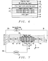
- a MTJ structure has a bottom spin valve configuration in which both of the free layer 36 and pinned layer 40 are comprised of one or more glassing agents, and preferably at least two glassing agents within each layer.
- the free layer 36 composition and interfaces 71, 72 with tunnel barrier layer and perpendicular Hk enhancing layer were previously described.
- the pinned layer 40 is comprised of at least three regions with a middle region 42 having a higher glassing agent concentration than that of lower region 41 and upper region 43.
- Glassing agent G is one of Mo, W, Si, Ta, P, Nb, Hf, Ti, Pd, Be, Cr, Zr, Cu, Os, V, or Mg and has a concentration from 1% to 30% in the pinned layer.
- B may be added as a second glassing agent in at least regions 33, 35 of the free layer and in regions 41, 43 of the pinned layer.
- pinned layer 40 may be comprised of CoFeB or an alloy of one or more of Co, Fe, Ni, and B.
- the three regions of the pinned layer 40 are distinct layers and the one or more glassing agents are introduced into at least the third region or middle layer 42 by a co-sputtering deposition process.
- a bottom layer 41 comprised of CoFeB or an alloy of one or more of Co, Fe, Ni, and B is deposited on a substrate such as a perpendicular Hk enhancing layer (not shown).
- a glassing agent G as described previously may be co-sputtered with a ferromagnetic alloy of one or more of Co, Fe, and Ni, or with an alloy of one or more of Co, Fe, Ni, and B to give a middle layer 42 with a CoFeG, CoFeNiG, CoBG, FeBG, CoFeBG, or CoFeNiBG composition wherein G is a second glassing agent and B is a first glassing agent.
- the upper layer 43 comprised of CoFeB or an alloy of one or more of Co, Fe, Ni, and B, for example, is sputter deposited on the middle layer.
- each of the lower and upper layers 41, 43 may be comprised of a plurality of n layers as explained earlier with respect to layers 33, 35 in free layer 36.
- the one or more glassing agents may be deposited in a separate process from the pinned layer ferromagnetic material deposition. Furthermore, one or more of the aforementioned glassing agents may be deposited in a laminated configuration wherein each glassing agent layer is from 0.1 to 5 Angstroms thick. According to this embodiment, a first CoFeB layer or an alloy of one or more of Co, Fe, Ni, and B may be deposited on a perpendicular Hk enhancing layer. Thereafter, one or more glassing agents are deposited in one or more layers to form a glassing agent layer or laminate on the first CoFeB layer or alloy layer.
- a second CoFeB layer or alloy of one or more of Co, Fe, Ni, and B is deposited on the glassing agent layer.
- one or more glassing agents from the middle glassing agent layer may diffuse into the adjoining CoFeB (or alloy) layers.
- the glassing agent G in the middle glassing agent layer forms nano-crystals along the grain boundaries of the adjoining CoFeB or alloy layers. The nano-crystals have a net magnetic moment of essentially zero.
- the perpendicular interfacial anisotropy in the first and second regions (layers) near the first and second interfaces dominates the shape anisotropy field and PMA is established in the free layer 36 and in pinned layer 40.
- regions 41, 43 have a lower glassing agent concentration than in the center region 42.
- the pinned layer (and free layer) configuration may be represented by CoFeBG/G/CoFeBG or alloyG/G/alloyG where the alloy has a CoFe, CoFeNi, CoB, FeB, or CoFeNiB composition.
- free layer 36 is part of a domain wall motion device.
- Pinned layer 31, tunnel barrier layer 32, perpendicular Hk enhancing layer 37, and capping layer 38 are also retained from previous embodiments.
- free layer 36 is comprised of regions 33-35 with a gradient of glassing agent concentration as described previously that increases from a second concentration at interfaces with layers 32, 37 to a first concentration at a middle region 34.
- the glassing agent concentration may increase in continuous increments from the second concentration to first concentration.
- regions 33-35 may be distinct layers such that free layer 36 is considered to be a composite structure.
- the MTJ stack is shown with a bottom spin valve structure and has a pinned layer/tunnel barrier/free layer/perpendicular Hk enhancing layer/capping layer configuration.
- pinned layer 31 has a width along an in-plane x-axis direction that is substantially less than the width of the overlying stack of layers.
- the stack of layers including tunnel barrier 32, free layer 36 comprised of regions 33-35, perpendicular Hk enhancing layer 37, and capping layer 38 may be patterned to provide a wire which from a top-down view (not shown) is part of an array of wires that are employed for storage of digital information.
- free layer 36 has a plurality of domain walls ( 75a - 75d) each extending vertically from a top surface that forms a first interface with layer 37 to a bottom surface which forms a second interface with tunnel barrier layer 32. There is a magnetic domain bounded by each pair of domain walls within the free layer.
- the number of domain walls is variable but is selected as four in the exemplary embodiment for illustrative purposes.
- the magnetic domain 92 aligned in a z-axis direction above pinned layer 31 has a switchable magnetization that changes from a (+) z-direction to a (-) z-direction or vice versa when a switching current is applied during a write process.
- free layer has two ends 45, 46 connected to a current/voltage source 81 in a first electrical loop including wiring 85a to a junction 82 to wire 83 and to end 45, and a wire 84 attached to end 46 to enable a write process.
- there is a second electrical loop which allows a readout of digital information in the switchable magnetic domain 92 during a read process.
- MTJ elements typically an array of MTJ elements (or domain wall motion devices) are fabricated on a substrate.
- the array of MTJ elements or the array of domain wall motion devices are connected by an array of wires that allow one or more of the MTJ elements or domain wall motion devices to be selectively written to or read to determine a memory state therein during a write process or read process, respectively.
- a top surface of a MTJ element may be connected to one or more adjacent MTJs (or domain wall motion devices) by one or more wires.
- the ferromagnetic or free layer serves as the storage layer since it is the magnetization direction of the ferromagnetic or free layer which determines whether the MTJ or domain wall motion device has a "0" or "1" magnetic state.
- VSM vibrating sample magnetometer
- Full film MTJ samples were prepared by sequentially forming a 50 Angstrom thick layer Ta seed layer, 3 Angstrom thick CoFeB layer, MgO tunnel barrier, free layer, MgO perpendicular Hk enhancing layer, and a Ru capping layer on a Si/SiO 2 substrate.
- the thin CoFeB layer formed on the Ta layer serves as a seed layer for MgO formation. Thickness of the CoFeB layer is only 3 Angstroms to minimize any magnetic contribution to the MTJ stack. All samples were annealed at 300°C for 1 hour.
- samples 60 and 62 conventional free layers are formed as a 14 Angstrom thick Co 20 Fe 60 B 20 film and a 16 Angstrom thick Co 20 Fe 60 B 20 film, respectively, which serve as a reference.
- the free layer in sample 61 was prepared by sequentially depositing a first 10 Angstrom thick Co 20 Fe 60 B 20 film, a 1.5 Angstrom thick Ta layer (less than one monolayer), and then a second 10 Angstrom thick Co 20 Fe 60 B 20 film according to an embodiment described herein.
- the free layer in sample 63 was prepared by sequentially depositing a five Angstrom thick Co 20 Fe 60 B 20 film, a 10 Angstrom thick Co 20 Fe 60 B 20 :Ta layer, and then a second Co 20 Fe 60 B 20 film that is 10 Angstroms thick according to another previously described embodiment.
- the middle layer contains about 20% Ta glassing agent. In all samples, the perpendicular interfacial anisotropy is strong enough to overcome the demagnetizing field so that the magnetization of the MTJ is pointing out of the plane of the film
- the data in FIG. 8 illustrate the benefit of a glassing agent (in this case Ta) in maintaining interfacial perpendicular anisotropy and reducing the crystalline anisotropy as a result of nano-crystalline character or an amorphous character in the middle layer of samples 61, 63, respectively.
- a glassing agent in this case Ta
- higher perpendicular anisotropy is achieved for a given magnetic moment.
- MTJ samples 61 and 62 have nearly the same moment but MTJ 61 has a considerably higher perpendicular anisotropy field.
- a higher magnetic moment is realized at the same perpendicular anisotropy field as indicated by a comparison of MTJ sample 63 to MTJ 62.
- All layers in the MTJs depicted in FIGS. 2 , 4-7 may be formed in an Anelva C-7100 thin film sputtering system or the like which typically includes three physical vapor deposition (PVD) chambers each having five targets, an oxidation chamber, and a sputter etching chamber. At least one of the PVD chambers is capable of co-sputtering.
- the sputter deposition process involves an argon sputter gas and the targets are made of metal or alloys to be deposited on a substrate.
- a high temperature annealing may be performed in a vacuum oven at a temperature of about 300°C to 400°C.
- an array of MTJ elements with substantially vertical sidewalls may be fabricated by a process involving a conventional photolithography patterning and ion etch sequence as is well known in the art and will not be described herein.
- an insulation layer may be deposited to electrically isolate adjacent MTJ elements.
- a chemical mechanical polish (CMP) process is typically employed to form a smooth surface of the insulation layer which becomes coplanar with a top surface of the MTJ array.
- additional metal levels such as a bit line layer may be formed on the MTJs to continue the fabrication of a magnetic device.
Landscapes
- Engineering & Computer Science (AREA)
- Chemical & Material Sciences (AREA)
- Crystallography & Structural Chemistry (AREA)
- Power Engineering (AREA)
- Nanotechnology (AREA)
- Physics & Mathematics (AREA)
- Spectroscopy & Molecular Physics (AREA)
- Manufacturing & Machinery (AREA)
- Computer Hardware Design (AREA)
- Mram Or Spin Memory Techniques (AREA)
- Hall/Mr Elements (AREA)
Claims (20)
- Un Elément de jonction tunnel magnétique (MTJ) comprenant une couche ferromagnétique (FL) comportant au moins deux interfaces produisant une anisotropie interfaciale perpendiculaire dominant un champ anisotropique de forme de la FL de telle manière qu'une direction magnétique est orientée hors du plan de la FL, comprenant :(a) une couche barrière à effet tunnel (32);(b) la couche ferromagnétique (36) qui a une première interface avec ladite couche barrière à effet tunnel et une seconde interface avec une couche d'amélioration de Hk perpendiculaire formée sur une surface de la couche ferromagnétique qui est opposée à une surface adjacente à la couche barrière à effet tunnel, la couche ferromagnétique comprend un agent de vitrage (G) constitué de Mo ou de W et ayant une première concentration inhibant la cristallisation et maintenant un caractère amorphe dans sa partie centrale (34), et une seconde concentration inférieure à la première concentration dans des parties (33) et (35) de la couche ferromagnétique situées à proximité des première et seconde interfaces; et(c) la couche d'amélioration de Hk perpendiculaire,caractérisé en ce que la couche barrière à effet tunnel et la couche d'amélioration de Hk perpendiculaire sont faites de MgO et la couche ferromagnétique est parmi CoFe, CoFeB, CoB, FeB ou CoFeBNi.
- L'élément MTJ de la revendication 1, dans lequel la teneur en agent de vitrage augmente progressivement depuis la deuxième concentration aux première et deuxième interfaces jusqu'à la première concentration dans la partie centrale de la couche ferromagnétique.
- L'élément MTJ de la revendication 1, dans lequel l'agent de vitrage (G) est déposé en une seule couche ou suivant une configuration stratifiée, dans laquelle chaque couche d'agent de vitrage présente une épaisseur comprise entre 0,1 à 5 Angströms.
- L'élément MTJ de la revendication 1, dans lequel la couche ferromagnétique est un composite d'une pluralité de couches, ou un alliage, et est dopée avec l'agent de vitrage (G) ayant une concentration d'environ 1% à 30% dans la couche ferromagnétique.
- L'élément MTJ de la revendication 4, dans lequel la couche ferromagnétique a une épaisseur d'environ 5 à 30 Angströms.
- L'élément MTJ de la revendication 1, comprenant en outre une couche de germination, une couche ancrée et une couche de recouvrement dans une configuration de vanne de spin inférieure dans laquelle la couche de germination, la couche ancrée, la couche barrière à effet tunnel, la couche libre, la couche d'amélioration de Hk perpendiculaire, et la couche de recouvrement sont séquentiellement formées sur un substrat.
- L'élément MTJ de la revendication 1, comprenant en outre une couche de germination, une couche ancrée et une couche de recouvrement dans une configuration de vanne de spin supérieure dans laquelle la couche de germination, la couche d'amélioration de Hk perpendiculaire, la couche libre, la couche barrière à effet tunnel, la couche ancrée et la couche de recouvrement sont formées séquentiellement sur un substrat.
- L'élément MTJ de la revendication 6, dans lequel la couche ancrée a une interface avec la couche barrière à effet tunnel et une interface avec la couche de germination, avec une première concentration d'agent de vitrage dans une partie centrale de la couche ancrée et une seconde concentration d'agent de vitrage dans des parties de la couche ancrée proches des interfaces avec la couche barrière à effet tunnel et la couche de germination.
- Un dispositif de mouvement de paroi de domaine, comprenant:(a) une couche magnétique ancrée (31) ayant une première largeur;(b) une barrière à effet tunnel (32) en contact avec une surface supérieure de la couche ancrée;(c) une couche libre (36) ayant une largeur sensiblement plus grande que la première largeur et formant une première interface avec la couche barrière à effet tunnel et une seconde interface avec une couche d'amélioration de Hk perpendiculaire (37) formée sur une surface de la couche libre qui est opposée à la surface sur la première interface, avec un agent de vitrage en Mo ou en W avec une première concentration présentant une cristallisation et qui maintient un caractère amorphe dans une partie centrale (34) de la couche libre et une seconde concentration inférieure à la première concentration dans des parties (33) et (35) de la couche libre proches des première et seconde interfaces, et dans lequel les parois de domaine (75a-75d) s'étendent verticalement entre les première et seconde interfaces pour établir des domaines magnétiques comprenant un domaine magnétique commutable aligné au-dessus de la couche magnétique ancrée; les première et seconde interfaces générant une anisotropie perpendiculaire interfaciale qui domine un champ anisotropique de forme de la couche libre de telle sorte qu'une direction de magnétisation (90a) est orientée hors du plan de la couche libre ;(d) la couche d'amélioration de Hk perpendiculaire; et(e) une couche de recouvrement (38) qui entre en contact avec une surface supérieure de la couche d'amélioration de Hk perpendiculaire, le dispositif de mouvement de paroi de domaine étant connecté électriquement à une source de courant/tension et à un dispositif de lecture pour permettre des processus de lecture et d'écriture ;caractérisé en ce que la barrière à effet tunnel et la couche d'amélioration de Hk perpendiculaire sont faites de MgO et la couche libre est parmi CoFe, CoFeB, CoB, FeB ou CoFeBNi.
Caractérisé en ce que la seconde concentration est supérieure à zéro et la couche libre est l'une parmi CoFe, CoFeB, CoB, FeB ou CoFeBNi. - Le dispositif de mouvement de paroi de domaine de la revendication 9, dans lequel la teneur en agent de vitrage augmente progressivement depuis la deuxième concentration aux première et deuxième interfaces jusqu'à la première concentration dans la partie centrale de la couche libre.
- Le dispositif de mouvement de paroi de domaine de la revendication 9, dans lequel l'agent de vitrage (G) est déposé sous forme d'une couche unique ou sous forme d'une configuration stratifiée, dans laquelle chaque couche d'agent de vitrage a une épaisseur de 0,1 à 5 Angströms.
- Dispositif de mouvement de paroi de domaine de la revendication 9, dans lequel la couche libre est un composite d'une pluralité de couches, et est dopée avec l'agent de vitrage (G) avec une concentration d'environ 1% à 30% dans la couche libre.
- Le dispositif de mouvement de paroi de domaine de la revendication 9, dans lequel la couche libre est une couche unique ou un empilement stratifié de couches ayant une épaisseur d'environ 5 à 30 Angströms.
- Le dispositif de mouvement de paroi de domaine de la revendication 9, dans lequel une surface supérieure de celle-ci est connectée à un ou plusieurs autres dispositifs de mouvement de paroi de domaine adjacents au moyen d'un ou plusieurs conducteurs afin de former une matrice, permettant ainsi à un ou plusieurs des dispositifs de mouvement de paroi de domaine d'être écrits ou lus, de manière sélective, respectivement au cours d'un processus d'écriture ou de lecture.
- Un procédé de formation d'un élément MTJ présentant une anisotropie perpendiculaire interfaciale au niveau d'une première interface (71) entre une couche libre et une couche barrière à effet tunnel adjacente (32) et au niveau d'une seconde interface (72) entre la couche libre et une couche d'amélioration de Hk perpendiculaire adjacente (37), l'anisotropie perpendiculaire interfaciale dominant un champ anisotropique de forme de la couche libre de telle sorte qu'une direction magnétique est orientée hors du plan de la couche libre, ledit procédé comprenant les étapes consistant à:a) former une couche ancrée (31) formée sur un substrat (28);(b) former une couche barrière à effet tunnel sur la couche ancrée;(c) déposer une couche libre ayant une surface inférieure qui forme une première interface avec une surface supérieure de ladite barrière à effet tunnel et ayant une surface supérieure qui forme une seconde interface avec une couche d'amélioration de Hk perpendiculaire déposée ultérieurement, la couche libre comprenant un agent de vitrage constitué de Mo ou de W avec une première concentration dans sa partie centrale qui cristallise à une première température, et une seconde concentration d'agent de vitrage inférieure à la première concentration dans les parties supérieure et inférieure de la couche ferromagnétique proche des première et seconde interfaces, de telle sorte que les parties supérieure et inférieure cristallisent à une deuxième température supérieure à la première température;(d) former la couche d'amélioration de Hk perpendiculaire sur la couche libre;(e) former une couche de recouvrement (38) qui entre en contact avec une surface supérieure de la couche d'amélioration de Hk perpendiculaire; et(f) effectuer un processus de recuitcaractérisé en ce que la concentration de la barrière à effet tunnel et de la couche d'amélioration de Hk perpendiculaire sont en MgO et la couche libre est parmi CoFe, CoFeB, CoB, FeB ou CoFeBNi.
- Le procédé de la revendication 15, dans lequel le processus de recuit est effectué à une température inférieure à la première température et supérieure à la seconde température.
- Le procédé de la revendication 15, dans lequel l'agent de vitrage (G) est formé avec une concentration comprise entre environ 1% et 30% dans la couche libre.
- Le procédé de la revendication 15, dans lequel l'agent de vitrage (G) est déposé en une seule couche ou en tant que configuration stratifiée dans laquelle chaque couche d'agent de vitrage a une épaisseur de 0,1 à 5 Angströms.
- Le procédé de la revendication 15, dans lequel la couche libre est un composite avec une pluralité de couches, une ou plusieurs couches contenant l'agent de vitrage (G) et les couches adjacentes aux première et deuxième interfaces ont une concentration en agent de vitrage (G) inférieure à celle d'une couche proche du milieu de la couche libre.
- Le procédé de la revendication 15, dans lequel la couche libre est une couche unique ou un empilement stratifié de couches constituées d'un alliage d'un ou de plusieurs éléments parmi Co, Fe, Ni et B d'une épaisseur comprise entre environ 5 et 30 Angströms, ou est un alliage d'un ou plusieurs de Co, Fe et Ni avec une épaisseur d'environ 5 à 30 Angströms.
Applications Claiming Priority (1)
| Application Number | Priority Date | Filing Date | Title |
|---|---|---|---|
| US13/548,859 US8698260B2 (en) | 2012-02-29 | 2012-07-13 | Engineered magnetic layer with improved perpendicular anisotropy using glassing agents for spintronic applications |
Publications (2)
| Publication Number | Publication Date |
|---|---|
| EP2873079A1 EP2873079A1 (fr) | 2015-05-20 |
| EP2873079B1 true EP2873079B1 (fr) | 2019-12-04 |
Family
ID=48857003
Family Applications (1)
| Application Number | Title | Priority Date | Filing Date |
|---|---|---|---|
| EP13740162.6A Active EP2873079B1 (fr) | 2012-07-13 | 2013-07-12 | Couche magnétique modifiée ayant une anisotropie perpendiculaire améliorée utilisant des agents vitrifiants pour des applications spintroniques |
Country Status (3)
| Country | Link |
|---|---|
| US (1) | US8698260B2 (fr) |
| EP (1) | EP2873079B1 (fr) |
| WO (1) | WO2014011950A1 (fr) |
Families Citing this family (37)
| Publication number | Priority date | Publication date | Assignee | Title |
|---|---|---|---|---|
| US8946834B2 (en) * | 2012-03-01 | 2015-02-03 | Headway Technologies, Inc. | High thermal stability free layer with high out-of-plane anisotropy for magnetic device applications |
| JP5765721B2 (ja) * | 2012-03-22 | 2015-08-19 | 国立研究開発法人物質・材料研究機構 | 高い垂直磁気異方性を示す極薄垂直磁化膜、その製造方法及び用途 |
| US9368176B2 (en) * | 2012-04-20 | 2016-06-14 | Alexander Mikhailovich Shukh | Scalable magnetoresistive element |
| US9461242B2 (en) * | 2013-09-13 | 2016-10-04 | Micron Technology, Inc. | Magnetic memory cells, methods of fabrication, semiconductor devices, memory systems, and electronic systems |
| US9214625B2 (en) * | 2014-03-18 | 2015-12-15 | International Business Machines Corporation | Thermally assisted MRAM with increased breakdown voltage using a double tunnel barrier |
| US9281466B2 (en) | 2014-04-09 | 2016-03-08 | Micron Technology, Inc. | Memory cells, semiconductor structures, semiconductor devices, and methods of fabrication |
| KR101549625B1 (ko) * | 2014-04-18 | 2015-09-04 | 한양대학교 산학협력단 | 메모리 소자 |
| US9324939B2 (en) | 2014-07-01 | 2016-04-26 | Qualcomm Incorporated | Synthetic antiferromagnet (SAF) coupled free layer for perpendicular magnetic tunnel junction (p-MTJ) |
| US9559296B2 (en) | 2014-07-03 | 2017-01-31 | Samsung Electronics Co., Ltd. | Method for providing a perpendicular magnetic anisotropy magnetic junction usable in spin transfer torque magnetic devices using a sacrificial insertion layer |
| US9444035B2 (en) * | 2014-09-10 | 2016-09-13 | Qualcomm Incorporated | Magnesium oxide capping with a shorted path for perpendicular magnetic tunnel junction devices and method for fabrication |
| US9620706B2 (en) | 2014-12-02 | 2017-04-11 | Qualcomm Incorporated | Magnetic etch stop layer for spin-transfer torque magnetoresistive random access memory magnetic tunnel junction device |
| KR102465539B1 (ko) | 2015-09-18 | 2022-11-11 | 삼성전자주식회사 | 자기 터널 접합 구조체를 포함하는 반도체 소자 및 그의 형성 방법 |
| US10134808B2 (en) | 2015-11-02 | 2018-11-20 | Qualcomm Incorporated | Magnetic tunnel junction (MTJ) devices with heterogeneous free layer structure, particularly suited for spin-torque-transfer (STT) magnetic random access memory (MRAM) (STT MRAM) |
| US10833253B2 (en) | 2016-02-05 | 2020-11-10 | International Business Machines Corporation | Low magnetic moment materials for spin transfer torque magnetoresistive random access memory devices |
| US20170263679A1 (en) * | 2016-03-11 | 2017-09-14 | Kabushiki Kaisha Toshiba | Magnetic memory device |
| US9893273B2 (en) | 2016-04-08 | 2018-02-13 | International Business Machines Corporation | Light element doped low magnetic moment material spin torque transfer MRAM |
| US10043607B2 (en) | 2016-05-02 | 2018-08-07 | International Business Machines Corporation | Electrolessly formed high resistivity magnetic materials |
| US10475564B2 (en) | 2016-06-29 | 2019-11-12 | Taiwan Semiconductor Manufacturing Company, Ltd. | Perpendicularly magnetized ferromagnetic layers having an oxide interface allowing for improved control of oxidation |
| US10635970B2 (en) * | 2016-08-04 | 2020-04-28 | International Business Machines Corporation | Racetrack synapse for neuromorphic applications |
| US10153423B2 (en) * | 2017-01-06 | 2018-12-11 | SK Hynix Inc. | Electronic device |
| US9966529B1 (en) | 2017-03-17 | 2018-05-08 | Headway Technologies, Inc. | MgO insertion into free layer for magnetic memory applications |
| JP2018157161A (ja) * | 2017-03-21 | 2018-10-04 | 東芝メモリ株式会社 | 磁気記憶装置及びその製造方法 |
| US11189781B2 (en) * | 2017-07-10 | 2021-11-30 | Everspin Technologies, Inc. | Magnetoresistive stack/structure including metal insertion substance |
| US11264290B2 (en) | 2017-09-06 | 2022-03-01 | Tdk Corporation | Tunnel magnetoresistive effect element and magnetic memory |
| US10665773B2 (en) * | 2018-01-26 | 2020-05-26 | Taiwan Semiconductor Manufacturing Company, Ltd. | Nitride capping layer for spin torque transfer (STT)-magnetoresistive random access memory (MRAM) |
| US10802087B2 (en) | 2018-09-11 | 2020-10-13 | Honeywell International Inc. | Spintronic accelerometer |
| US10871529B2 (en) | 2018-09-11 | 2020-12-22 | Honeywell International Inc. | Spintronic mechanical shock and vibration sensor device |
| US10876839B2 (en) * | 2018-09-11 | 2020-12-29 | Honeywell International Inc. | Spintronic gyroscopic sensor device |
| US10797225B2 (en) * | 2018-09-18 | 2020-10-06 | Taiwan Semiconductor Manufacturing Company, Ltd. | Dual magnetic tunnel junction (DMTJ) stack design |
| US10950782B2 (en) | 2019-02-14 | 2021-03-16 | Headway Technologies, Inc. | Nitride diffusion barrier structure for spintronic applications |
| US11264566B2 (en) | 2019-06-21 | 2022-03-01 | Headway Technologies, Inc. | Magnetic element with perpendicular magnetic anisotropy (PMA) and improved coercivity field (Hc)/switching current ratio |
| KR20230012371A (ko) * | 2021-07-15 | 2023-01-26 | 삼성전자주식회사 | 자기터널접합 소자 및 자기터널접합 소자를 포함하는 메모리 장치 |
| KR102906616B1 (ko) * | 2021-07-15 | 2025-12-30 | 삼성전자주식회사 | 자기터널접합 소자 및 자기터널접합 소자를 포함하는 메모리 장치 |
| US12150387B2 (en) | 2021-07-15 | 2024-11-19 | Samsung Electronics Co., Ltd. | Magnetic tunneling junction device and memory device including the same |
| EP4358139A4 (fr) * | 2021-08-19 | 2024-07-31 | Huawei Technologies Co., Ltd. | Dispositif magnétique et son procédé de fabrication, mémoire magnétique et dispositif électronique |
| US12266384B2 (en) * | 2023-01-05 | 2025-04-01 | Headway Technologies, Inc. | Tunneling magnetoresistance device with magnetically soft high moment free layer |
| US20250364006A1 (en) * | 2024-05-24 | 2025-11-27 | Headway Technologies, Inc. | High Unidirectional Anisotropy Constant Amorphous Shield Layer For Shield Application |
Family Cites Families (15)
| Publication number | Priority date | Publication date | Assignee | Title |
|---|---|---|---|---|
| US6166948A (en) | 1999-09-03 | 2000-12-26 | International Business Machines Corporation | Magnetic memory array with magnetic tunnel junction memory cells having flux-closed free layers |
| US6614630B2 (en) | 2001-04-23 | 2003-09-02 | Headway Technologies, Inc. | Top spin valve heads for ultra-high recording density |
| TWI222630B (en) | 2001-04-24 | 2004-10-21 | Matsushita Electric Industrial Co Ltd | Magnetoresistive element and magnetoresistive memory device using the same |
| US7394626B2 (en) * | 2002-11-01 | 2008-07-01 | Nec Corporation | Magnetoresistance device with a diffusion barrier between a conductor and a magnetoresistance element and method of fabricating the same |
| US20050264952A1 (en) * | 2004-05-28 | 2005-12-01 | Fujitsu Limited | Magneto-resistive element, magnetic head and magnetic storage apparatus |
| US7351483B2 (en) | 2004-11-10 | 2008-04-01 | International Business Machines Corporation | Magnetic tunnel junctions using amorphous materials as reference and free layers |
| US7285835B2 (en) | 2005-02-24 | 2007-10-23 | Freescale Semiconductor, Inc. | Low power magnetoelectronic device structures utilizing enhanced permeability materials |
| US8063459B2 (en) * | 2007-02-12 | 2011-11-22 | Avalanche Technologies, Inc. | Non-volatile magnetic memory element with graded layer |
| US8593862B2 (en) | 2007-02-12 | 2013-11-26 | Avalanche Technology, Inc. | Spin-transfer torque magnetic random access memory having magnetic tunnel junction with perpendicular magnetic anisotropy |
| US20090122450A1 (en) * | 2007-11-08 | 2009-05-14 | Headway Technologies, Inc. | TMR device with low magnetostriction free layer |
| JP4764466B2 (ja) | 2008-09-25 | 2011-09-07 | 株式会社東芝 | ホイスラー合金を有する積層体、この積層体を用いた磁気抵抗素子、及びスピントランジスタ |
| US8183653B2 (en) | 2009-07-13 | 2012-05-22 | Seagate Technology Llc | Magnetic tunnel junction having coherent tunneling structure |
| US8913350B2 (en) | 2009-08-10 | 2014-12-16 | Grandis, Inc. | Method and system for providing magnetic tunneling junction elements having improved performance through capping layer induced perpendicular anisotropy and memories using such magnetic elements |
| JP5177585B2 (ja) | 2010-09-17 | 2013-04-03 | 株式会社東芝 | 磁気抵抗効果素子及び磁気メモリ |
| US8912614B2 (en) * | 2011-11-11 | 2014-12-16 | International Business Machines Corporation | Magnetic tunnel junction devices having magnetic layers formed on composite, obliquely deposited seed layers |
-
2012
- 2012-07-13 US US13/548,859 patent/US8698260B2/en active Active
-
2013
- 2013-07-12 WO PCT/US2013/050190 patent/WO2014011950A1/fr not_active Ceased
- 2013-07-12 EP EP13740162.6A patent/EP2873079B1/fr active Active
Non-Patent Citations (1)
| Title |
|---|
| None * |
Also Published As
| Publication number | Publication date |
|---|---|
| US8698260B2 (en) | 2014-04-15 |
| EP2873079A1 (fr) | 2015-05-20 |
| WO2014011950A1 (fr) | 2014-01-16 |
| US20130221460A1 (en) | 2013-08-29 |
Similar Documents
| Publication | Publication Date | Title |
|---|---|---|
| EP2873079B1 (fr) | Couche magnétique modifiée ayant une anisotropie perpendiculaire améliorée utilisant des agents vitrifiants pour des applications spintroniques | |
| EP2820680B1 (fr) | Couche magnétique manipulée à anisotropie perpendiculaire améliorée au moyen d'agents de vitrification pour des applications spintroniques | |
| US11930717B2 (en) | Minimal thickness synthetic antiferromagnetic (SAF) structure with perpendicular magnetic anisotropy for STT-MRAM | |
| US11672182B2 (en) | Seed layer for multilayer magnetic materials | |
| EP2705518B1 (fr) | Couches multiples ayant un champ de démagnétisation perpendiculaire réduit en utilisant un moment de dilution pour des applications spintroniques | |
| EP2673807B1 (fr) | Élément magnétique à anisotropie hors du plan améliorée pour applications spintroniques | |
| EP2987190B1 (fr) | Jonction tunnel magnétique comprenant un antiferro-aimant synthétique complètement compensé pour applications de spintronique | |
| US20140217530A1 (en) | Co/Ni Multilayers with Improved Out-of-Plane Anisotropy for Magnetic Device Applications | |
| CN112838160B (zh) | 磁性结、磁性装置和用于提供磁性结的方法 | |
| CN104733606B (zh) | 一种具有双层优化层的磁电阻元件 | |
| CN104766923B (zh) | 一种三层结构记忆层的磁电阻元件 | |
| CN204481057U (zh) | 一种具有单层辅助层的磁电阻元件 | |
| CN204481055U (zh) | 一种具有多层辅助层的磁电阻元件 |
Legal Events
| Date | Code | Title | Description |
|---|---|---|---|
| PUAI | Public reference made under article 153(3) epc to a published international application that has entered the european phase |
Free format text: ORIGINAL CODE: 0009012 |
|
| 17P | Request for examination filed |
Effective date: 20150210 |
|
| AK | Designated contracting states |
Kind code of ref document: A1 Designated state(s): AL AT BE BG CH CY CZ DE DK EE ES FI FR GB GR HR HU IE IS IT LI LT LU LV MC MK MT NL NO PL PT RO RS SE SI SK SM TR |
|
| AX | Request for extension of the european patent |
Extension state: BA ME |
|
| DAX | Request for extension of the european patent (deleted) | ||
| STAA | Information on the status of an ep patent application or granted ep patent |
Free format text: STATUS: EXAMINATION IS IN PROGRESS |
|
| 17Q | First examination report despatched |
Effective date: 20181004 |
|
| GRAP | Despatch of communication of intention to grant a patent |
Free format text: ORIGINAL CODE: EPIDOSNIGR1 |
|
| STAA | Information on the status of an ep patent application or granted ep patent |
Free format text: STATUS: GRANT OF PATENT IS INTENDED |
|
| INTG | Intention to grant announced |
Effective date: 20190627 |
|
| GRAS | Grant fee paid |
Free format text: ORIGINAL CODE: EPIDOSNIGR3 |
|
| GRAA | (expected) grant |
Free format text: ORIGINAL CODE: 0009210 |
|
| STAA | Information on the status of an ep patent application or granted ep patent |
Free format text: STATUS: THE PATENT HAS BEEN GRANTED |
|
| AK | Designated contracting states |
Kind code of ref document: B1 Designated state(s): AL AT BE BG CH CY CZ DE DK EE ES FI FR GB GR HR HU IE IS IT LI LT LU LV MC MK MT NL NO PL PT RO RS SE SI SK SM TR |
|
| REG | Reference to a national code |
Ref country code: GB Ref legal event code: FG4D |
|
| REG | Reference to a national code |
Ref country code: CH Ref legal event code: EP |
|
| REG | Reference to a national code |
Ref country code: AT Ref legal event code: REF Ref document number: 1210422 Country of ref document: AT Kind code of ref document: T Effective date: 20191215 |
|
| REG | Reference to a national code |
Ref country code: DE Ref legal event code: R096 Ref document number: 602013063595 Country of ref document: DE |
|
| REG | Reference to a national code |
Ref country code: IE Ref legal event code: FG4D |
|
| REG | Reference to a national code |
Ref country code: NL Ref legal event code: MP Effective date: 20191204 |
|
| REG | Reference to a national code |
Ref country code: LT Ref legal event code: MG4D |
|
| PG25 | Lapsed in a contracting state [announced via postgrant information from national office to epo] |
Ref country code: LT Free format text: LAPSE BECAUSE OF FAILURE TO SUBMIT A TRANSLATION OF THE DESCRIPTION OR TO PAY THE FEE WITHIN THE PRESCRIBED TIME-LIMIT Effective date: 20191204 Ref country code: NO Free format text: LAPSE BECAUSE OF FAILURE TO SUBMIT A TRANSLATION OF THE DESCRIPTION OR TO PAY THE FEE WITHIN THE PRESCRIBED TIME-LIMIT Effective date: 20200304 Ref country code: GR Free format text: LAPSE BECAUSE OF FAILURE TO SUBMIT A TRANSLATION OF THE DESCRIPTION OR TO PAY THE FEE WITHIN THE PRESCRIBED TIME-LIMIT Effective date: 20200305 Ref country code: ES Free format text: LAPSE BECAUSE OF FAILURE TO SUBMIT A TRANSLATION OF THE DESCRIPTION OR TO PAY THE FEE WITHIN THE PRESCRIBED TIME-LIMIT Effective date: 20191204 Ref country code: BG Free format text: LAPSE BECAUSE OF FAILURE TO SUBMIT A TRANSLATION OF THE DESCRIPTION OR TO PAY THE FEE WITHIN THE PRESCRIBED TIME-LIMIT Effective date: 20200304 Ref country code: FI Free format text: LAPSE BECAUSE OF FAILURE TO SUBMIT A TRANSLATION OF THE DESCRIPTION OR TO PAY THE FEE WITHIN THE PRESCRIBED TIME-LIMIT Effective date: 20191204 Ref country code: LV Free format text: LAPSE BECAUSE OF FAILURE TO SUBMIT A TRANSLATION OF THE DESCRIPTION OR TO PAY THE FEE WITHIN THE PRESCRIBED TIME-LIMIT Effective date: 20191204 Ref country code: SE Free format text: LAPSE BECAUSE OF FAILURE TO SUBMIT A TRANSLATION OF THE DESCRIPTION OR TO PAY THE FEE WITHIN THE PRESCRIBED TIME-LIMIT Effective date: 20191204 |
|
| PG25 | Lapsed in a contracting state [announced via postgrant information from national office to epo] |
Ref country code: HR Free format text: LAPSE BECAUSE OF FAILURE TO SUBMIT A TRANSLATION OF THE DESCRIPTION OR TO PAY THE FEE WITHIN THE PRESCRIBED TIME-LIMIT Effective date: 20191204 Ref country code: RS Free format text: LAPSE BECAUSE OF FAILURE TO SUBMIT A TRANSLATION OF THE DESCRIPTION OR TO PAY THE FEE WITHIN THE PRESCRIBED TIME-LIMIT Effective date: 20191204 |
|
| PG25 | Lapsed in a contracting state [announced via postgrant information from national office to epo] |
Ref country code: AL Free format text: LAPSE BECAUSE OF FAILURE TO SUBMIT A TRANSLATION OF THE DESCRIPTION OR TO PAY THE FEE WITHIN THE PRESCRIBED TIME-LIMIT Effective date: 20191204 |
|
| PG25 | Lapsed in a contracting state [announced via postgrant information from national office to epo] |
Ref country code: PT Free format text: LAPSE BECAUSE OF FAILURE TO SUBMIT A TRANSLATION OF THE DESCRIPTION OR TO PAY THE FEE WITHIN THE PRESCRIBED TIME-LIMIT Effective date: 20200429 Ref country code: CZ Free format text: LAPSE BECAUSE OF FAILURE TO SUBMIT A TRANSLATION OF THE DESCRIPTION OR TO PAY THE FEE WITHIN THE PRESCRIBED TIME-LIMIT Effective date: 20191204 Ref country code: RO Free format text: LAPSE BECAUSE OF FAILURE TO SUBMIT A TRANSLATION OF THE DESCRIPTION OR TO PAY THE FEE WITHIN THE PRESCRIBED TIME-LIMIT Effective date: 20191204 Ref country code: NL Free format text: LAPSE BECAUSE OF FAILURE TO SUBMIT A TRANSLATION OF THE DESCRIPTION OR TO PAY THE FEE WITHIN THE PRESCRIBED TIME-LIMIT Effective date: 20191204 Ref country code: EE Free format text: LAPSE BECAUSE OF FAILURE TO SUBMIT A TRANSLATION OF THE DESCRIPTION OR TO PAY THE FEE WITHIN THE PRESCRIBED TIME-LIMIT Effective date: 20191204 |
|
| PG25 | Lapsed in a contracting state [announced via postgrant information from national office to epo] |
Ref country code: SK Free format text: LAPSE BECAUSE OF FAILURE TO SUBMIT A TRANSLATION OF THE DESCRIPTION OR TO PAY THE FEE WITHIN THE PRESCRIBED TIME-LIMIT Effective date: 20191204 Ref country code: IS Free format text: LAPSE BECAUSE OF FAILURE TO SUBMIT A TRANSLATION OF THE DESCRIPTION OR TO PAY THE FEE WITHIN THE PRESCRIBED TIME-LIMIT Effective date: 20200404 Ref country code: SM Free format text: LAPSE BECAUSE OF FAILURE TO SUBMIT A TRANSLATION OF THE DESCRIPTION OR TO PAY THE FEE WITHIN THE PRESCRIBED TIME-LIMIT Effective date: 20191204 |
|
| REG | Reference to a national code |
Ref country code: DE Ref legal event code: R097 Ref document number: 602013063595 Country of ref document: DE |
|
| REG | Reference to a national code |
Ref country code: AT Ref legal event code: MK05 Ref document number: 1210422 Country of ref document: AT Kind code of ref document: T Effective date: 20191204 |
|
| PLBE | No opposition filed within time limit |
Free format text: ORIGINAL CODE: 0009261 |
|
| STAA | Information on the status of an ep patent application or granted ep patent |
Free format text: STATUS: NO OPPOSITION FILED WITHIN TIME LIMIT |
|
| PG25 | Lapsed in a contracting state [announced via postgrant information from national office to epo] |
Ref country code: DK Free format text: LAPSE BECAUSE OF FAILURE TO SUBMIT A TRANSLATION OF THE DESCRIPTION OR TO PAY THE FEE WITHIN THE PRESCRIBED TIME-LIMIT Effective date: 20191204 |
|
| 26N | No opposition filed |
Effective date: 20200907 |
|
| PG25 | Lapsed in a contracting state [announced via postgrant information from national office to epo] |
Ref country code: AT Free format text: LAPSE BECAUSE OF FAILURE TO SUBMIT A TRANSLATION OF THE DESCRIPTION OR TO PAY THE FEE WITHIN THE PRESCRIBED TIME-LIMIT Effective date: 20191204 Ref country code: PL Free format text: LAPSE BECAUSE OF FAILURE TO SUBMIT A TRANSLATION OF THE DESCRIPTION OR TO PAY THE FEE WITHIN THE PRESCRIBED TIME-LIMIT Effective date: 20191204 Ref country code: SI Free format text: LAPSE BECAUSE OF FAILURE TO SUBMIT A TRANSLATION OF THE DESCRIPTION OR TO PAY THE FEE WITHIN THE PRESCRIBED TIME-LIMIT Effective date: 20191204 |
|
| PG25 | Lapsed in a contracting state [announced via postgrant information from national office to epo] |
Ref country code: IT Free format text: LAPSE BECAUSE OF FAILURE TO SUBMIT A TRANSLATION OF THE DESCRIPTION OR TO PAY THE FEE WITHIN THE PRESCRIBED TIME-LIMIT Effective date: 20191204 |
|
| REG | Reference to a national code |
Ref country code: DE Ref legal event code: R082 Ref document number: 602013063595 Country of ref document: DE Representative=s name: 2K PATENTANWAELTE BLASBERG KEWITZ & REICHEL PA, DE Ref country code: DE Ref legal event code: R081 Ref document number: 602013063595 Country of ref document: DE Owner name: TAIWAN SEMICONDUCTOR MANUFACTURING COMPANY, LT, TW Free format text: FORMER OWNER: HEADWAY TECHNOLOGIES, INC., MILPITAS, CALIF., US |
|
| PG25 | Lapsed in a contracting state [announced via postgrant information from national office to epo] |
Ref country code: MC Free format text: LAPSE BECAUSE OF FAILURE TO SUBMIT A TRANSLATION OF THE DESCRIPTION OR TO PAY THE FEE WITHIN THE PRESCRIBED TIME-LIMIT Effective date: 20191204 |
|
| REG | Reference to a national code |
Ref country code: CH Ref legal event code: PL |
|
| GBPC | Gb: european patent ceased through non-payment of renewal fee |
Effective date: 20200712 |
|
| REG | Reference to a national code |
Ref country code: BE Ref legal event code: MM Effective date: 20200731 |
|
| PG25 | Lapsed in a contracting state [announced via postgrant information from national office to epo] |
Ref country code: LU Free format text: LAPSE BECAUSE OF NON-PAYMENT OF DUE FEES Effective date: 20200712 Ref country code: FR Free format text: LAPSE BECAUSE OF NON-PAYMENT OF DUE FEES Effective date: 20200731 Ref country code: LI Free format text: LAPSE BECAUSE OF NON-PAYMENT OF DUE FEES Effective date: 20200731 Ref country code: GB Free format text: LAPSE BECAUSE OF NON-PAYMENT OF DUE FEES Effective date: 20200712 Ref country code: CH Free format text: LAPSE BECAUSE OF NON-PAYMENT OF DUE FEES Effective date: 20200731 |
|
| PG25 | Lapsed in a contracting state [announced via postgrant information from national office to epo] |
Ref country code: BE Free format text: LAPSE BECAUSE OF NON-PAYMENT OF DUE FEES Effective date: 20200731 |
|
| PG25 | Lapsed in a contracting state [announced via postgrant information from national office to epo] |
Ref country code: IE Free format text: LAPSE BECAUSE OF NON-PAYMENT OF DUE FEES Effective date: 20200712 |
|
| PG25 | Lapsed in a contracting state [announced via postgrant information from national office to epo] |
Ref country code: TR Free format text: LAPSE BECAUSE OF FAILURE TO SUBMIT A TRANSLATION OF THE DESCRIPTION OR TO PAY THE FEE WITHIN THE PRESCRIBED TIME-LIMIT Effective date: 20191204 Ref country code: MT Free format text: LAPSE BECAUSE OF FAILURE TO SUBMIT A TRANSLATION OF THE DESCRIPTION OR TO PAY THE FEE WITHIN THE PRESCRIBED TIME-LIMIT Effective date: 20191204 Ref country code: CY Free format text: LAPSE BECAUSE OF FAILURE TO SUBMIT A TRANSLATION OF THE DESCRIPTION OR TO PAY THE FEE WITHIN THE PRESCRIBED TIME-LIMIT Effective date: 20191204 |
|
| PG25 | Lapsed in a contracting state [announced via postgrant information from national office to epo] |
Ref country code: MK Free format text: LAPSE BECAUSE OF FAILURE TO SUBMIT A TRANSLATION OF THE DESCRIPTION OR TO PAY THE FEE WITHIN THE PRESCRIBED TIME-LIMIT Effective date: 20191204 |
|
| PGFP | Annual fee paid to national office [announced via postgrant information from national office to epo] |
Ref country code: DE Payment date: 20250729 Year of fee payment: 13 |