EP2874477B1 - Carte de câblage - Google Patents
Carte de câblage Download PDFInfo
- Publication number
- EP2874477B1 EP2874477B1 EP13821782.3A EP13821782A EP2874477B1 EP 2874477 B1 EP2874477 B1 EP 2874477B1 EP 13821782 A EP13821782 A EP 13821782A EP 2874477 B1 EP2874477 B1 EP 2874477B1
- Authority
- EP
- European Patent Office
- Prior art keywords
- layer
- connecting terminal
- width
- wiring board
- principal surface
- Prior art date
- Legal status (The legal status is an assumption and is not a legal conclusion. Google has not performed a legal analysis and makes no representation as to the accuracy of the status listed.)
- Not-in-force
Links
Images






Classifications
-
- H—ELECTRICITY
- H05—ELECTRIC TECHNIQUES NOT OTHERWISE PROVIDED FOR
- H05K—PRINTED CIRCUITS; CASINGS OR CONSTRUCTIONAL DETAILS OF ELECTRIC APPARATUS; MANUFACTURE OF ASSEMBLAGES OF ELECTRICAL COMPONENTS
- H05K1/00—Printed circuits
- H05K1/18—Printed circuits structurally associated with non-printed electric components
- H05K1/181—Printed circuits structurally associated with non-printed electric components associated with surface mounted components
-
- H—ELECTRICITY
- H05—ELECTRIC TECHNIQUES NOT OTHERWISE PROVIDED FOR
- H05K—PRINTED CIRCUITS; CASINGS OR CONSTRUCTIONAL DETAILS OF ELECTRIC APPARATUS; MANUFACTURE OF ASSEMBLAGES OF ELECTRICAL COMPONENTS
- H05K3/00—Apparatus or processes for manufacturing printed circuits
- H05K3/22—Secondary treatment of printed circuits
- H05K3/28—Applying non-metallic protective coatings
-
- H—ELECTRICITY
- H05—ELECTRIC TECHNIQUES NOT OTHERWISE PROVIDED FOR
- H05K—PRINTED CIRCUITS; CASINGS OR CONSTRUCTIONAL DETAILS OF ELECTRIC APPARATUS; MANUFACTURE OF ASSEMBLAGES OF ELECTRICAL COMPONENTS
- H05K3/00—Apparatus or processes for manufacturing printed circuits
- H05K3/40—Forming printed elements for providing electric connections to or between printed circuits
- H05K3/4007—Surface contacts, e.g. bumps
-
- H—ELECTRICITY
- H10—SEMICONDUCTOR DEVICES; ELECTRIC SOLID-STATE DEVICES NOT OTHERWISE PROVIDED FOR
- H10W—GENERIC PACKAGES, INTERCONNECTIONS, CONNECTORS OR OTHER CONSTRUCTIONAL DETAILS OF DEVICES COVERED BY CLASS H10
- H10W70/00—Package substrates; Interposers; Redistribution layers [RDL]
- H10W70/60—Insulating or insulated package substrates; Interposers; Redistribution layers
-
- H—ELECTRICITY
- H10—SEMICONDUCTOR DEVICES; ELECTRIC SOLID-STATE DEVICES NOT OTHERWISE PROVIDED FOR
- H10W—GENERIC PACKAGES, INTERCONNECTIONS, CONNECTORS OR OTHER CONSTRUCTIONAL DETAILS OF DEVICES COVERED BY CLASS H10
- H10W70/00—Package substrates; Interposers; Redistribution layers [RDL]
- H10W70/60—Insulating or insulated package substrates; Interposers; Redistribution layers
- H10W70/62—Insulating or insulated package substrates; Interposers; Redistribution layers characterised by their interconnections
- H10W70/65—Shapes or dispositions of interconnections
- H10W70/652—Cross-sectional shapes
- H10W70/6525—Cross-sectional shapes for securing the interconnections to the substrate, e.g. to prevent peeling
-
- H—ELECTRICITY
- H05—ELECTRIC TECHNIQUES NOT OTHERWISE PROVIDED FOR
- H05K—PRINTED CIRCUITS; CASINGS OR CONSTRUCTIONAL DETAILS OF ELECTRIC APPARATUS; MANUFACTURE OF ASSEMBLAGES OF ELECTRICAL COMPONENTS
- H05K1/00—Printed circuits
- H05K1/02—Details
- H05K1/11—Printed elements for providing electric connections to or between printed circuits
- H05K1/111—Pads for surface mounting, e.g. lay-out
- H05K1/112—Pads for surface mounting, e.g. lay-out directly combined with via connections
- H05K1/113—Via provided in pad; Pad over filled via
-
- H—ELECTRICITY
- H05—ELECTRIC TECHNIQUES NOT OTHERWISE PROVIDED FOR
- H05K—PRINTED CIRCUITS; CASINGS OR CONSTRUCTIONAL DETAILS OF ELECTRIC APPARATUS; MANUFACTURE OF ASSEMBLAGES OF ELECTRICAL COMPONENTS
- H05K2201/00—Indexing scheme relating to printed circuits covered by H05K1/00
- H05K2201/09—Shape and layout
- H05K2201/09209—Shape and layout details of conductors
- H05K2201/09654—Shape and layout details of conductors covering at least two types of conductors provided for in H05K2201/09218 - H05K2201/095
- H05K2201/09672—Superposed layout, i.e. in different planes
-
- H—ELECTRICITY
- H05—ELECTRIC TECHNIQUES NOT OTHERWISE PROVIDED FOR
- H05K—PRINTED CIRCUITS; CASINGS OR CONSTRUCTIONAL DETAILS OF ELECTRIC APPARATUS; MANUFACTURE OF ASSEMBLAGES OF ELECTRICAL COMPONENTS
- H05K2201/00—Indexing scheme relating to printed circuits covered by H05K1/00
- H05K2201/09—Shape and layout
- H05K2201/09209—Shape and layout details of conductors
- H05K2201/09654—Shape and layout details of conductors covering at least two types of conductors provided for in H05K2201/09218 - H05K2201/095
- H05K2201/098—Special shape of the cross-section of conductors, e.g. very thick plated conductors
-
- H—ELECTRICITY
- H05—ELECTRIC TECHNIQUES NOT OTHERWISE PROVIDED FOR
- H05K—PRINTED CIRCUITS; CASINGS OR CONSTRUCTIONAL DETAILS OF ELECTRIC APPARATUS; MANUFACTURE OF ASSEMBLAGES OF ELECTRICAL COMPONENTS
- H05K2201/00—Indexing scheme relating to printed circuits covered by H05K1/00
- H05K2201/20—Details of printed circuits not provided for in H05K2201/01 - H05K2201/10
- H05K2201/2072—Anchoring, i.e. one structure gripping into another
-
- H—ELECTRICITY
- H05—ELECTRIC TECHNIQUES NOT OTHERWISE PROVIDED FOR
- H05K—PRINTED CIRCUITS; CASINGS OR CONSTRUCTIONAL DETAILS OF ELECTRIC APPARATUS; MANUFACTURE OF ASSEMBLAGES OF ELECTRICAL COMPONENTS
- H05K2203/00—Indexing scheme relating to apparatus or processes for manufacturing printed circuits covered by H05K3/00
- H05K2203/05—Patterning and lithography; Masks; Details of resist
- H05K2203/0562—Details of resist
- H05K2203/0597—Resist applied over the edges or sides of conductors, e.g. for protection during etching or plating
-
- H—ELECTRICITY
- H05—ELECTRIC TECHNIQUES NOT OTHERWISE PROVIDED FOR
- H05K—PRINTED CIRCUITS; CASINGS OR CONSTRUCTIONAL DETAILS OF ELECTRIC APPARATUS; MANUFACTURE OF ASSEMBLAGES OF ELECTRICAL COMPONENTS
- H05K3/00—Apparatus or processes for manufacturing printed circuits
- H05K3/30—Assembling printed circuits with electric components, e.g. with resistors
- H05K3/32—Assembling printed circuits with electric components, e.g. with resistors electrically connecting electric components or wires to printed circuits
- H05K3/34—Assembling printed circuits with electric components, e.g. with resistors electrically connecting electric components or wires to printed circuits by soldering
- H05K3/341—Surface mounted components
- H05K3/3431—Leadless components
- H05K3/3436—Leadless components having an array of bottom contacts, e.g. pad grid array or ball grid array components
-
- H—ELECTRICITY
- H05—ELECTRIC TECHNIQUES NOT OTHERWISE PROVIDED FOR
- H05K—PRINTED CIRCUITS; CASINGS OR CONSTRUCTIONAL DETAILS OF ELECTRIC APPARATUS; MANUFACTURE OF ASSEMBLAGES OF ELECTRICAL COMPONENTS
- H05K3/00—Apparatus or processes for manufacturing printed circuits
- H05K3/46—Manufacturing multilayer circuits
- H05K3/4602—Manufacturing multilayer circuits characterized by a special circuit board as base or central core whereon additional circuit layers are built or additional circuit boards are laminated
-
- H—ELECTRICITY
- H10—SEMICONDUCTOR DEVICES; ELECTRIC SOLID-STATE DEVICES NOT OTHERWISE PROVIDED FOR
- H10W—GENERIC PACKAGES, INTERCONNECTIONS, CONNECTORS OR OTHER CONSTRUCTIONAL DETAILS OF DEVICES COVERED BY CLASS H10
- H10W70/00—Package substrates; Interposers; Redistribution layers [RDL]
- H10W70/60—Insulating or insulated package substrates; Interposers; Redistribution layers
- H10W70/67—Insulating or insulated package substrates; Interposers; Redistribution layers characterised by their insulating layers or insulating parts
- H10W70/68—Shapes or dispositions thereof
- H10W70/685—Shapes or dispositions thereof comprising multiple insulating layers
Definitions
- the present invention relates to a wiring board that includes a plurality of connecting terminals on a principal surface for connecting to a semiconductor chip.
- a terminal for connection to a semiconductor chip (hereinafter referred to as a connecting terminal) is formed on a principal surface (front face) of a wiring board.
- a connecting terminal is formed on a principal surface (front face) of a wiring board.
- the density of the connecting terminals has been becoming high, and therefore the distance (pitch) of the arranged connecting terminals has been narrow.
- a wiring board adopting a Non-Solder Mask Defined (NSMD) shape where a plurality of connecting terminals is disposed in the same opening of a solder resist has been proposed.
- the connecting terminals are disposed at narrow pitches in the same opening, a solder coated on the surface of the connecting terminal possibly flows out to adjacent connecting terminals, resulting in a short circuit between the connecting terminals. Since the connecting terminals are disposed at high density, the wiring widths of the connecting terminals become narrow. Accordingly, there is a possibility that the connecting terminals cannot obtain sufficient adhesion strength. In this case, the connecting terminal may be fallen over or peeled off under fabrication process.
- Patent Document 1 JP-A-2011-192692
- the connecting terminal may be fallen over or peeled off under fabrication process until the solder resist is filled up between the connecting terminals.
- the present invention has been made to solve the above-described circumstances.
- the present invention aims to provide a wiring board that ensures adhesion strength of the connecting terminals to reduce the connecting terminal from being fallen over or peeled off under fabrication process.
- WO 2012/056883 A1 discloses a wiring board according to the preamble of claim 1.
- the present invention provides a wiring board with a laminated body where one or more layer of each of an insulating layer and a conductor layer are laminated.
- the wiring board includes a plurality of connecting terminals formed separately from one another on the laminated body, a filling member filled up between the plurality of connecting terminals.
- the filling member is filled up to a position lower than a height of the plurality of connecting terminals.
- the connecting terminal has a cross section with a trapezoidal shape where a width of a first principal surface on a side contacting the laminated body is wider than a width of a second principal surface facing the first principal surface.
- the connecting terminal has the first principal surface that includes a contact surface and spaced surfaces.
- the contact surface contacts the laminated body.
- the spaced surfaces are disposed on both ends of the contact surface and not in contact with the laminated body.
- the cross sections of the connecting terminals which are formed separately from one another on the laminated body, has a trapezoidal shape where the width of the first principal surface on the side contacting the laminated body is wider than the width of the second principal surface facing the first principal surface.
- the trapezoidal cross sectional shape of the connecting terminal inhibits generation of a void between the connecting terminal and the filling member. Furthermore, the width of the second principal surface of the connecting terminal is narrow. This inhibits the solder coated on the surface of the connecting terminal to flow out to adjacent connecting terminals and inhibits causing a short circuit between the connecting terminals.
- the contact surface has a width wider than a width of the second principal surface. Since the width of the contact surface is wider than the width of the second principal surface, this ensures sufficient adhesion strength. This reduces the connecting terminal from being fallen over or peeled off under fabrication process.
- the filling member functions as a solder resist.
- the filling member that functions as the solder resist reduces a solder from remaining on the filling member, thus reducing a short circuit between the connecting terminals.
- a solder resist layer is provided on the laminate body.
- the solder resist layer has openings that expose the plurality of connecting terminals.
- the solder resist layer covers a wiring pattern connected to the plurality of connecting terminals.
- the wiring pattern has a cross section with a trapezoidal shape where a width of a third principal surface on a side contacting the laminated body is wider than a width of a fourth principal surface facing the third principal surface.
- At least a part of the plurality of connecting terminals has a ratio of a width of the first principal surface with respect to a width of the second principal surface larger than a ratio of width of the third principal surface with respect to a width of the fourth principal surface of the wiring pattern.
- the width of the second principal surface of the connecting terminal becomes narrow.
- a distance between the connecting terminals is lengthened.
- a short circuit between the connecting terminals can be further efficiently inhibited.
- the width of the fourth principal surface of the wiring pattern becomes large, the cross sectional area of the wiring becomes large. This ensures a low electrical resistance of the wiring pattern.
- a wiring board that ensures adhesion strength of the connecting terminal to reduce the connecting terminal from being fallen over or peeled off under fabrication process can be provided.
- the wiring board is only necessary to include a plurality of connecting terminals whose top surface and the side surfaces are exposed.
- the wiring board may be, for example, formed without a core substrate.
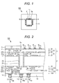
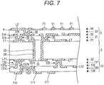
- Fig. 1 is a top view (front face side) of a wiring board 100 according to a first embodiment.
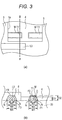
- Fig. 2 is a partial sectional view of the wiring board 100 taken along the line I-I of Fig. 1 .
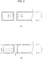
- Fig. 3 is a configuration diagram of connecting terminals T1 and a metal wiring L3 (wiring pattern) on the front face side of the wiring board 100.
- Fig. 3A is a top view.
- Fig. 3B is a sectional view taken along the line II-II of Fig. 3A .
- a side to which a semiconductor chip is connected is referred to as a front face side while a side to which a motherboard, a socket, or a similar member (hereinafter referred to as a motherboard or a similar member) is connected is referred to as a reverse face side.
- the connecting terminal T1 and the metal wiring L3 constitute a conductor layer 34.
- the wiring board 100 illustrated in Fig. 1 to Fig. 3 includes a core substrate 2, a buildup layer 3 (front face side), a filling member 4, a solder resist layer 5, a buildup layer 13 (reverse face side), and a solder resist layer 14.
- the buildup layer 3 includes the plurality of connecting terminals T1 for connection to a semiconductor chip (not shown).
- the buildup layer 3 is laminated on the front face side of the core substrate 2.
- the filling member 4 is laminated on the front surface side of the buildup layer 3.
- the filling member 4 fills up between the plurality of connecting terminals T1.
- the solder resist layer 5 is laminated on the front surface side of the filling member 4.
- the solder resist layer 5 includes an opening 5a to expose the plurality of connecting terminals T1.
- the buildup layer 13 includes a plurality of connecting terminals T11 for connection to a motherboard or a similar member (not shown).
- the buildup layer 13 is laminated on the reverse face side of the core substrate 2.
- the solder resist layer 14 is laminated on the reverse face side of the buildup layer 13.
- the solder resist layer 14 includes an opening 14a to at least partially expose the connecting terminal T11.
- the core substrate 2 is a plate-shaped substrate made of resin.
- the core substrate 2 is constituted of a heat-resistant resin plate (for example, a bismaleimide-triazine resin plate), a fiber reinforced resin plate (for example, a glass fiber reinforced epoxy resin), or a similar plate.
- the core substrate 2 includes core conductor layers 21 and 22, which form metal wirings L1 and L11, on the respective front face and reverse face.
- the core substrate 2 includes a through-hole 23 drilled by a drill or similar tool.
- a through-hole conductor 24 is formed on the inner wall surface of the through-hole 23.
- the through-hole conductor 24 conducts the core conductor layers 21 and 22 to one another.
- the through-hole 23 is filled up with a resin-made plug 25 made of resin such as epoxy resin.
- the buildup layer 3 includes resin insulating layers 31 and 33 and conductor layers 32 and 34 laminated on the front face side of the core substrate 2.
- the resin insulating layer 31 is made of thermosetting resin composition.
- the conductor layer 32 is formed on the surface of the resin insulating layer 31.
- the conductor layer 32 forms a metal wiring L2.
- a via 35 that electrically connects the core conductor layer 21 and the conductor layer 32 is formed in the resin insulating layer 31.
- the resin insulating layer 33 is made of thermosetting resin composition.
- the conductor layer 34 is formed on the surface layer of the resin insulating layer 33.
- the conductor layer 34 includes the plurality of connecting terminals T1.
- a via 36 that electrically connects the conductor layer 32 and the conductor layer 34 is formed in the insulating layer 33.
- the resin insulating layers 31 and 33 and the conductor layer 32 constitute a laminated body.
- the vias 35 and 36 include a via hole 37a, a via conductor 37b, a via pad 37c, and a via land 37d.
- the via conductor 37b is disposed on the inner peripheral surface of the via hole 37a.
- the via pad 37c is disposed so as to be conducted with the via conductor 37b at the bottom surface side.
- the via land 37d is disposed on the opposite side of the via pad 37c.
- the via land 37d outwardly projects from the opening peripheral edge of the via conductor 37b.
- the connecting terminal T1 is a connecting terminal for connection to the semiconductor chip.
- the connecting terminal T1 is a so-called peripheral connecting terminal disposed along the inner peripheral of the mounting region for the semiconductor chip.
- the semiconductor chip is mounted on the wiring board 100.
- Each connecting terminal T1 has a rough surface to improve an adhesive property with the filling member 4, which will be described below.
- each connecting terminal T1 has a trapezoidal shape where a width W1 is wider than a width W2.
- the width W1 is a width of a first principal surface F1 on the side contacting a laminated body constituted by the resin insulating layers 31 and 33 and the conductor layer 32.
- the width W2 is a width of a second principal surface F2 facing the first principal surface F1.
- the first principal surface F1 of the connecting terminal T1 includes a contact surface C, which contacts the laminated body, and spaced surfaces N.
- the spaced surfaces N are disposed at both ends of the contact surface C and do not contact the laminated body.
- a width W3 of the contact surface C is wider than the width W2 of the second principal surface F2.
- the metal wiring L3 (wiring pattern) is covered with the solder resist layer 5.
- the cross section of the metal wiring L3 (wiring pattern) has a trapezoidal shape where a width W4 is wider than a width W5.
- the width W4 is a width of a third principal surface F3 on the side contacting the laminated body.
- the width W5 is a width of a fourth principal surface F4 facing the third principal surface F3.
- the third principal surface F3 of the metal wiring L3 (wiring pattern) includes the contact surface C, which contacts the laminated body, and spaced surfaces N.
- the spaced surfaces N are disposed at both ends of the contact surface C and do not contact the laminated body.
- a width W6 of the contact surface C is wider than the width W5 of the fourth principal surface F4.
- At least a part of the plurality of connecting terminals T1 has a ratio W1/W2 larger than a ratio W4/W5.
- the ratio W1/W2 is a ratio of the width W1 of the first principal surface F1 with respect to the width W2 of the second principal surface F2.
- the ratio W4/W5 is a ratio of the width W4 of the third principal surface F3 with respect to the width W5 of the fourth principal surface F4 of the metal wiring L3 (wiring pattern).
- each of the connecting terminals T1 is covered with a metal plating layer M.
- the metal plating layer M is constituted of, for example, a single layer selected from metal layers such as a Ni layer, a Sn layer, an Ag layer, a Pd layer, and an Au layer, or a plurality of layers (such as, Ni layer/Au layer, and Ni layer/Pd layer/Au layer).
- a rustproof Organic Solderability Preservative (OSP) process may be performed instead of the metal plating layer M.
- a solder may be coated on the exposed surface of the connecting terminal T1. Furthermore, after covering the exposed surface of the connecting terminal T1 with the metal plating layer M, the metal plating layer M may be coated with the solder. A method for coating the solder on the exposed surface of the connecting terminal T1 will be described later.
- the filling member 4 is an insulating member laminated on the buildup layer 3.
- the material of the filling member 4 is preferred to be the same as a material of the solder resist layer 5.
- the filling member 4 is filled up between the connecting terminals T1 while contacting the side surface of each connecting terminal T1 formed on the surface layer of the buildup layer 3.
- a thickness D1 of the filling member 4 is thinner than a thickness (height) D2 of the connecting terminal T1.
- the solder resist layer 5 covers the wiring pattern connected to the connecting terminal T1 and includes the opening 5a.
- the opening 5a exposes the connecting terminal T1 disposed along the inner peripheral of the mounting region for the semiconductor chip.
- the opening 5a of the solder resist layer 5 forms an NSMD shape where the plurality of connecting terminals T1 are disposed in the same opening.
- the buildup layer 13 includes resin insulating layers 131 and 133 and conductor layers 132 and 134 laminated on the reverse face side of the core substrate 2.
- the resin insulating layer 131 is made of thermosetting resin composition.
- the conductor layer 132 including a metal wiring L12 is formed on the reverse face of the resin insulating layer 131.
- a via 135 that electrically connects the core conductor layer 22 and the conductor layer 132 is formed in the resin insulating layer 131.
- the resin insulating layer 133 is made of thermosetting resin composition.
- the conductor layer 134 that includes one or more connecting terminal T11 is formed on the surface layer of the resin insulating layer 133.
- a via 136 that electrically connects the conductor layer 132 and conductor layer 134 is formed in the resin insulating layer 133.
- Vias 135 and 136 include a via hole 137a, a via conductor 137b, a via pad 137c, and a via land 137d.
- the via conductor 137b is disposed at the inner peripheral surface of the via hole 137a.
- the via pad 137c is disposed so as to be conducted with the via conductor 137b at the bottom surface side.
- the via land 137d is disposed on the opposite side of the via pad 137c.
- the via land 137d outwardly projects from the opening peripheral edge of the via conductor 137b.
- the connecting terminal T11 is used as a reverse face land (PGA pad, BGA pad) to connect the wiring board 100 to a motherboard or a similar member.
- the connecting terminal T11 is formed at the outer peripheral region of the wiring board 100 excluding its approximate center portion and arranged in a rectangular shape so as to surround the approximate center portion. At least a part of the surface of the connecting terminal T11 is covered with the metal plating layer M.
- the solder resist layer 14 is formed by laminating a film solder resist on the surface of the buildup layer 13.
- the solder resist layer 14 includes the opening 14a that partially exposes the surface of each connecting terminal T11.
- the surface of each connecting terminal T11 is partially exposed from the solder resist layer 14 by the opening 14a. That is, the opening 14a of the solder resist layer 14 is formed to have a Solder Mask Defined (SMD) shape where the surface of each connecting terminal T11 is partially exposed. Different from the opening 5a of the solder resist layer 5, the opening 14a of the solder resist layer 14 is formed at each connecting terminal T11.
- SMD Solder Mask Defined
- a solder ball B made of a solder, such as Sn-Ag, Sn-Cu, Sn-Ag-Cu, and Sn-Sb that substantially do not contain Pb is formed in the opening 14a.
- the solder ball B is formed to electrically connect to the connecting terminal T11 via the metal plating layer M.
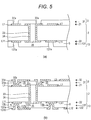
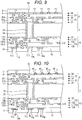
- Fig. 4 to Fig. 10 are process drawings for fabricating the wiring board 100 according to the first embodiment. The following describes methods for fabricating the wiring board 100 with reference to Fig. 4 to Fig. 10 .
- a copper-clad laminate which includes a plate-shaped substrate made of resin to which copper foils are pasted on the front face and the reverse face, is prepared.
- the copper-clad laminate is drilled with a drill to preliminarily form a penetration hole, which will be the through-hole 23, at a predetermined position.
- the through-hole conductor 24 is formed on the inner wall of the through-hole 23 by performing electroless copper plating and electrolytic copper plating in accordance with a conventionally known method.
- copper plating layers are formed on both surfaces of the copper-clad laminate (see Fig. 4A ).
- the inside of the through-hole conductor 24 is filled up with the resin plug 25 such as epoxy resin. Furthermore, the copper plating layer formed on the copper foils of both surfaces of the copper-clad laminate is etched to a desired shape. Thus, the core conductor layers 21 and 22 forming the metal wirings L1 and L11 on the respective front face and reverse face of the copper-clad laminate are formed, thus obtaining the core substrate 2 (see Fig. 4B ). After forming the through-hole 23, performing a desmear process, which removes a smear at a processed part, is preferred.
- Film insulating resin materials having main constituent of epoxy resin are disposed overlapping with one another on the front face and the reverse face of the core substrate 2 to form resin insulating layers 31 and 131. Then, this laminated product is pressed and heated with a vacuum thermocompression bonding machine, and the film insulating resin materials are press-bonded with heat hardening. Next, laser irradiation is performed using a conventionally well-known laser processing apparatus to form the via holes 37a and 137a at the respective resin insulating layers 31 and 131 (see Fig. 5A ).
- electroless copper plating is performed to form electroless copper plating layers on the resin insulating layers 31 and 131 including the inner walls of the via holes 37a and 137a.
- a photoresist is laminated on the electroless copper plating layers formed on the resin insulating layers 31 and 131 and then is exposed and developed to form a desired-shaped plating resist.
- the copper is plated by electrolytic plating to obtain a desired copper plating pattern.
- the plating resist is peeled off and the electroless copper plating layer, which was present under the plating resist, is removed to form the conductor layers 32 and 132 forming the metal wirings L2 and L12.
- the vias 35 and 135 including the via conductors 37b and 137b, the via pads 37c and 137c, and the via lands 37d and 137d are formed (see Fig. 5B ).
- film insulating resin materials having main constituent of epoxy resin are disposed overlapping with one another on the conductor layers 32 and 132 to form the resin insulating layers 33 and 133. Then, this laminated product is pressed and heated with a vacuum thermocompression bonding machine, and the film insulating resin materials are press-bonded with heat hardening. Next, laser irradiation is performed using a conventionally well-known laser processing apparatus to form the via holes 37a and 137a at the respective resin insulating layers 33 and 133 (see Fig. 6A ).
- the conductor layers 34 and 134 with connecting terminals T1 and T11 and the vias 36 and 136 are formed on the respective resin insulating layers 33 and 133 with the via holes 37a and 137a (see Fig. 6B ).
- the surfaces of the connecting terminal T1 can be roughened, for example, by processing using etchant, such as MEC-Etch-Bond (manufactured by MEC Company Ltd.).
- etchant such as MEC-Etch-Bond (manufactured by MEC Company Ltd.).
- the first filling up method thinly coats a thermosetting insulating resin on the surface of the buildup layer 3 including the connecting terminal T1 on the surface layer, performs heat hardening, and then polishes the hardened insulating resin until being lower than the top surface of the connecting terminals T1.
- the filling member 4 should not be removed to the extent that the surface of the resin insulating layer 33, which is a foundation layer, is exposed.
- the second filling up method thinly coats a thermosetting insulating resin on the surface of the buildup layer 3 including the connecting terminal T1 on the surface layer, removes extra insulating resin covering the top surface of the connecting terminals T1 with solvent that melts the insulating resin, and then performs heat hardening on the insulating resin. It is noted that the filling member 4 should not be removed to the extent that the surface of the resin insulating layer 33, which is a foundation layer, is exposed.
- the third filling up method thickly coats a thermosetting insulating resin on the surface of the buildup layer 3 with the connecting terminal T1 on the surface layer, performs heat hardening, masks the region other than the mounting region for the semiconductor device, and then dry-etches the insulating resin by, for example, Reactive Ion Etching (RIE) until being lower than the top surface of the connecting terminals T1.
- RIE Reactive Ion Etching
- the filling member 4 and the solder resist layer 5 are integrally formed. It is noted that the filling member 4 should not be removed to the extent that the surface of the resin insulating layer 33, which is a foundation layer, is exposed.
- Fig. 8 is an explanatory view of a fourth filling up method.
- the following describes the fourth filling up method with reference to Fig. 8 .
- the fourth filling up method thickly coats a photocurable insulating resin on the surface of the buildup layer 3 including the wiring conductor T1 on the surface layer (see Fig. 8A ), masks the inner region of the region, which will be the opening 5a of the solder resist layer later, and exposes and develops the insulating resin.
- the insulating resin which will be the outer region of the opening 5a, is photo-cured (see Fig. 8B ).
- the wiring board 100 under fabrication is immersed in a sodium carbonate solution (concentration: 1 weight%) for a short period (period to the extent that the insulating-resin surface of the unexposed portion is slightly swelled) (see Fig. 8C ).
- the insulating resin swelled is emulsified by water washing (see Fig. 8D ).
- the swelled and emulsified insulating resin is removed from the wiring board 100 under fabrication (see Fig. 8E ).
- the immersion and the water washing are performed by one time respectively or repeated by several times respectively until the upper end position of the insulating resin that has not been photo-cured is positioned lower than the top surface of each connecting terminal T1.
- the insulating resin is hardened by heat or ultraviolet rays.
- the filling member 4 should not be removed to the extent that the surface of the resin insulating layer 33, which is a foundation layer, is exposed.
- the filling member 4 and the solder resist layer 5 are integrally formed.
- Film solder resists are pressed and laminated on the surfaces of the filling member 4 and the conductor layer 134.
- the laminated film solder resists are exposed and developed to obtain the solder resist layer 5 with the NSMD-shaped opening 5a and the solder resist layer 14 with the SMD-shaped opening 14a.
- the opening 5a exposes the surface and the side surfaces of the plurality of connecting terminals T1 while the opening 14a exposes a part of the surface of each connecting terminal T11.
- the solder resist layer 5 does not have to be laminated at the process.
- the exposed surface of the connecting terminal T1 is etched using, for example, sodium persulfate to remove impurities, for example, an oxide film on the surface of the connecting terminal T1.
- a step is formed around the principal surface (outer periphery) of the connecting terminal T1 by ething.
- the metal plating layer M is formed on the exposed surfaces of the connecting terminals T1 and T11 by performing electroless reduction plating using a reduction agent.
- the metal plating layer M is formed on the exposed surface of the connecting terminal T1 by the electroless substitution plating, the metal on the exposed surface of the connecting terminal T1 is substituted, thus forming the metal plating layer M.
- the step is formed around the principal surface of the connecting terminal T1.
- solder is coated on the exposed surface of the connecting terminal T1
- the following two methods can be selected according to the thickness of the solder layer to be coated.
- the solder layer with a thickness of 5 to 30 ⁇ m is coated on the exposed surface of the connecting terminal T1
- the exposed surface of the connecting terminal T1 is etched little (soft etching) to remove the oxide film formed on the exposed surface of the connecting terminal T1.
- the step is formed around the principal surface of the connecting terminal T1.
- a paste for example, super solder (product name) of Harima Chemicals Group, Inc.
- a flux is thinly applied over the entire inside of the NSMD-shaped opening 5a so as to cover the entire exposed surface of the connecting terminal T1.
- reflow is performed to form a solder layer made of an alloy containing Sn and Ag, or Sn, Ag, and Cu on the exposed surface of the connecting terminal T1.
- the solder layer with a thickness of equal to or less than 10 ⁇ m is coated on the exposed surface of the connecting terminal T1
- the exposed surface of the connecting terminal T1 is etched little (soft etching) to remove the oxide film formed at the exposed surface of the connecting terminal T1.
- the step is formed around the principal surface of the connecting terminal T1.
- electroless tin (Sn) plating is performed on the exposed surface of the connecting terminal T1 to form an Sn plating layer, and the flux is applied so as to cover the entire surface of the Sn plating layer.
- a reflow is performed to melt the Sn plating layer plated on the connecting terminal T1 so as to form the solder layer on the principal surface of the connecting terminal T1.
- the melted Sn is condensed to the principal surface of the connecting terminal T1 by surface tension.
- solder paste is applied over the metal plating layer M formed on the connecting terminal T11 by solder printing, a reflow is performed at a predetermined temperature for a predetermined period, and the solder ball B is formed on the connecting terminal T11, thus the wiring board 100 illustrated in Fig. 1 and Fig. 2 is obtained.
- each connecting terminal T1 has a trapezoidal shape where the width W1 is wider than the width W2.
- the width W1 is the width of the first principal surface F1 on the side contacting the laminated body constituted by the resin insulating layers 31 and 33 and the conductor layer 32.
- the width W2 is the width of the second principal surface F2 facing the first principal surface F1.
- the first principal surface F1 of the connecting terminal T1 includes the contact surface C, which contacts the laminated body, and the spaced surfaces N.
- the spaced surfaces N are disposed at both ends of the contact surface C and do not contact the laminated body.
- the width W3 of the contact surface C is wider than the width W2 of the second principal surface F2.
- the area of the connecting terminal T1 contacting the laminated body becomes large, thus ensures to obtain sufficient adhesion strength. This reduces the connecting terminal T1 from being fallen over or peeled off under fabrication process.
- the trapezoidal cross sectional shape of the connecting terminal T1 inhibits generation of a void between the connecting terminal T1 and the filling member 4. Furthermore, the width W2 of the second principal surface F2 of the connecting terminal T1 is narrow. This inhibits the solder coated on the surface of the connecting terminal T1 to flow out to adjacent connecting terminals T1 and inhibits a short circuit caused between the connecting terminals T 1.
- the first principal surface F1 of the connecting terminal T1 includes the contact surface C, which contacts the laminated body, and the spaced surfaces N.
- the spaced surfaces N are disposed at both ends of the contact surface C and do not contact the laminated body.
- the width W3 of the contact surface C is wider than the width W2 of the second principal surface F2. This ensures sufficient adhesion strength. This reduces the connecting terminal from being fallen over or peeled off under fabrication process.
- the wiring board 100 of the embodiment at least a part of the plurality of connecting terminals T1 has the ratio W1/W2 larger than the ratio W4/W5.
- the ratio W1/W2 is a ratio of the width W1 of the first principal surface F1 with respect to the width W2 of the second principal surface F2.
- the ratio W4/W5 is a ratio of the width W4 of the third principal surface F3 with respect to the width W5 of the fourth principal surface F4 of the metal wiring L3 (wiring pattern).
- the above-described configuration narrows the width W2 of the second principal surface F2 of the connecting terminal T1, thus a distance between the connecting terminals T1 is lengthened. In view of this, a short circuit between the connecting terminals T1 can be further efficiently inhibited. Since the width W5 of the fourth principal surface F4 of the metal wiring L3 (wiring pattern) becomes large, the cross sectional area of the metal wiring L3 (wiring pattern) becomes large. This ensures a low electrical resistance of the metal wiring L3 (wiring pattern).
- the filling member 4 is filled up between the roughened connecting terminals T1, the adhesion strength between the connecting terminals T1 and the filling member 4 is improved. In view of this, peel-off of the connecting terminal 1 under fabrication process can be further efficiently inhibited.
- Use of the material same as the material of the solder resist layer 5 for the filling member 4 makes flowability of the solder of the filling member 4 to the same extent as that of the solder resist layer 5. This inhibits the solder from remaining on the filling member 4 and from resulting in a short circuit between the connecting terminals T1.
- the thickness D1 of the filling member 4 filled up between the connecting terminals T1 is thinner than the thickness (height) D2 of the connecting terminal T1. That is, the connecting terminal T1 slightly protrudes from the top surface of the filling member 4. In view of this, even if the center of the connecting terminal of the semiconductor chip is misaligned with the center of the connecting terminal T1, the connecting terminal of the semiconductor chip contacts the end portion of the connecting terminal T1, thus connection reliability between the connecting terminal T1 and the connecting terminal of the semiconductor chip is improved.
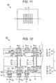
- Fig. 11 is a top view (front face side) of a wiring board 200 according to the second embodiment.
- Fig. 12 is a partial sectional view of the wiring board 200 taken along the line I-I of Fig. 11 .
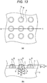
- Fig. 13 is a configuration diagram of a connecting terminal T2 on the front face side of the wiring board 200.
- Fig. 13A is a top view of the connecting terminal T2.
- Fig. 13B is a sectional view taken along the line II-II of Fig. 13A .
- a configuration of the wiring board 200 will now be described with reference to Fig. 11 to Fig. 13 , wherein the same reference numerals designate corresponding or identical elements with the wiring board 100 described with reference to Fig. 1 to Fig. 3 throughout the embodiments, and the repeated description will be omitted correspondingly.
- the wiring board 200 includes a lid plating layer 41 that electrically connects to the core conductor layer 21 on the front face side.
- the lid plating layer 41 and the conductor layer 32 are electrically connected with a filled via 42 while the conductor layer 32 and the conductor layer 34 are electrically connected with a filled via 43.
- the filled vias 42 and 43 include a via hole 44a and a via conductor 44b filled up inside of the via hole 44a by plating.
- the buildup layer 3 includes only a connecting terminal T2 (described later) at the outer most layer.
- the buildup layer 3 does not include a wiring pattern connected at the same layer as the connecting terminal T2 and a solder resist layer that covers the wiring pattern.
- the resin insulating layers 31 and 33 and the conductor layer 32 constitute a laminated body.
- the connecting terminal T2 formed on the front face side of the wiring board 200 is a so-called area bump type of connecting terminal disposed on the entire mounting region for the semiconductor chip.
- the connecting terminal T2 is a connecting terminal for the semiconductor chip.
- the semiconductor chip is mounted on the wiring board 200.
- Each connecting terminal T2 has a rough surface to improve an adhesive property with the filling member 4.
- the surfaces of the connecting terminal T2 can be roughened, for example, by processing using etchant, such as MEC-Etch-Bond (which is manufactured by MEC Company Ltd.).
- each connecting terminal T2 has a trapezoidal shape where the width W1 is wider than the width W2.
- the width W1 is the width of the first principal surface F1 on the side contacting the laminated body constituted by the resin insulating layers 31 and 33 and the conductor layer 32.
- the width W2 is the width of the second principal surface F2 facing the first principal surface F1.
- the first principal surface F1 of the connecting terminal T2 includes the contact surface C, which contacts the laminated body, and the spaced surfaces N.
- the spaced surfaces N are disposed at both ends of the contact surface C and do not contact the laminated body.
- the width W3 of the contact surface C is wider than the width W2 of the second principal surface F2.
- the exposed surface of the connecting terminal T2 is covered with the metal plating layer M.
- the connecting terminal of the semiconductor chip and the connecting terminal T2 are electrically connected by reflowing the solder coated on the connecting terminal of the semiconductor chip.
- a solder may be coated, or a rustproof OSP process may be performed.
- the metal plating layer M is formed on the connecting terminal T2 as follows.
- the exposed surface of the connecting terminal T2 is etched using, for example, sodium persulfate.
- the metal plating layer M is formed on the exposed surface of the connecting terminal T2 by performing electroless reduction plating using a reducing agent.
- etching using, for example, sodium persulfate a step is formed around the principal surface of the connecting terminal T2.
- the metal plating layer M is formed on the exposed surface of the connecting terminal T2 by the electroless substitution plating, the metal on the exposed surface of the connecting terminal T2 is substituted, thus forming the metal plating layer M.
- the step is formed around the principal surface of the connecting terminal T2.
- the plurality of connecting terminals T2 of the wiring board 200 projects from the resin insulating layer 33, and the surface and the side surfaces of the connecting terminals T2 are exposed.
- the filling member 4 which is an insulating member is filled up between the connection terminal.
- the thickness D1 of the filling member 4 is thinner than the thickness (height) D2 of the connecting terminal T2.
- the filling member 4 can be filled up between the connecting terminals T2 by the first to the fourth filling up methods described in the first embodiment.
- the wiring board 200 includes a lid plating layer 141 that electrically connects to the core conductor layer 22 on the reverse face side.
- the lid plating layer 141 and the conductor layer 132 are electrically connected with a filled via 142 while the conductor layer 132 and the conductor layer 134 are electrically connected with a filled via 143.
- the filled vias 142 and 143 include a via hole 144a and a via conductor 144b filled up inside of the via hole 144a by plating.
- the cross section of each connecting terminal T2 has a trapezoidal shape where the width W1 is wider than the width W2.
- the width W1 is the width of the first principal surface F1 on the side contacting the laminated body constituted by the resin insulating layers 31 and 33 and the conductor layer 32.
- the width W2 is the width of the second principal surface F2 facing the first principal surface F1.
- the wiring board 200 according to the second embodiment has the same effects as the effects of the wiring board 100 according to the first embodiment.
- Fig. 14 is a top view (front face side) of a wiring board 300 according to a third embodiment.
- Fig. 15 is a partial sectional view of the wiring board 300 taken along the line I-I of Fig. 14 .
- Fig. 16 is a configuration diagram of a connecting terminal T3 on the front face side of the wiring board 300.
- Fig. 16A is a top view of the connecting terminal T3.
- Fig. 16B is a sectional view taken along the line II-II of Fig. 16A .
- the wiring board 300 according to the third embodiment differs from the wiring board 200 described with reference to Fig. 11 to Fig. 13 in that the connecting terminals T3 and T11 are directly formed on the conductor layers 32 and 132 without through vias.
- a configuration of the wiring board 300 will now be described with reference to Fig. 14 to Fig. 16 , wherein the same reference numerals designate corresponding or identical elements with the wiring board 100 described with reference to Fig. 1 to Fig. 3 and the wiring board 200 described with reference to Fig. 11 to Fig. 13 throughout the embodiments, and the repeated description will be omitted correspondingly.
- the wiring board 300 includes the lid plating layer 41 that electrically connects to the core conductor layer 21 on the front surface side.
- the lid plating layer 41 and the conductor layer 32 are electrically connected with the filled via 42.
- the filled via 42 includes the via hole 44a and the via conductor 44b filled up inside of the via hole 44a by plating.
- the connecting terminals T3 formed on the conductor layer 32 of the wiring board 300 are disposed at approximately equal spacing and in a grid pattern on the entire mounting region for the semiconductor chip.
- the connecting terminal T3 has a pillar shape (for example, a column, a quadratic prism, and a triangular prism).
- the connecting terminal T3 is directly formed on the conductor layers 32 without through a via with the top portion projecting from the surface of the filling member 4.
- the connecting terminal T3 is a connecting terminal for the semiconductor chip.
- Each connecting terminal T3 has a rough surface to improve an adhesive property with the filling member 4.
- the surfaces of the connecting terminal T3 is processed, for example, using etchant, such as MEC-Etch-Bond (which is manufactured by MEC Company Ltd.).
- each connecting terminal T3 has a trapezoidal shape where the width W1 is wider than the width W2.
- the width W1 is the width of the first principal surface F1 on the side contacting the laminated body constituted by the resin insulating layers 31 and 33 and the conductor layer 32.
- the width W2 is the width of the second principal surface F2 facing the first principal surface F1.
- the first principal surface F1 of the connecting terminal T2 includes the contact surface C, which contacts the laminated body, and the spaced surfaces N.
- the spaced surfaces N are disposed at both ends of the contact surface C and do not contact the laminated body.
- the width W3 of the contact surface C is wider than the width W2 of the second principal surface F2.
- each connecting terminal T3 is covered with the metal plating layer M.
- the metal plating layer M is constituted of, for example, a single layer selected from metal layers such as a Ni layer, a Sn layer, an Ag layer, a Pd layer, and an Au layer, or a plurality of layers (for example, Ni layer/Au layer and Ni layer/Pd layer/Au layer).
- a rustproof Organic Solderability Preservative (OSP) process may be performed instead of the metal plating layer M.
- a solder may be coated on the exposed surface of the connecting terminal T3. Furthermore, after covering the exposed surface of the connecting terminal T3 with the metal plating layer M, the metal plating layer M may be coated with the solder.
- a method for coating the solder on the exposed surface of the connecting terminal T3 is described in the first embodiment, and the repeated description will be omitted correspondingly.
- the filling member 4 is filled up between the connecting terminals T3 while contacting the side surface of each connecting terminal T3 formed on the surface layer of the buildup layer 3.
- the thickness D1 of the filling member 4 is thinner than the thickness (height) D2 of the connecting terminal T3.
- the filling member 4 can be filled up between the connecting terminals T3 by the first to the fourth filling up methods described in the first embodiment.
- the solder resist layer 5 includes an opening 5b and an opening 5c.
- the opening 5b exposes the connecting terminals T3 disposed at approximately equal spacing on the mounting region for the semiconductor chip.
- the opening 5c exposes a pad P for mounting a chip capacitor.
- the opening 5b of the solder resist layer 5 forms an NSMD shape where the plurality of connecting terminals T3 are disposed in the same opening.
- An alignment mark AM is formed on the solder resist layer 5.
- the wiring board 300 has a configuration that includes the lid plating layer 141 that electrically connects to the core conductor layer 22 on the reverse face side.
- the lid plating layer 141 and the conductor layer 132 are electrically connected with the filled via 142.
- the filled via 142 includes the via hole 144a and the via conductor 144b filled up inside of the via hole 144a by plating.
- the connecting terminal T11 for connection to a motherboard or a similar member (not shown) is directly formed on the conductor layer 132 without through a via.
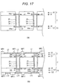
- Fig. 17 and Fig. 18 are process drawings for fabricating the wiring board 300 according to the third embodiment.
- the following describes methods for fabricating the wiring board 300 with reference to Fig. 17 and Fig. 18 . Since a core substrate process, a filling up process, a solder resist layer process, a plating process, and a back-end process are the same as the methods for fabricating the wiring board 100 according to the first embodiment described with reference to Fig. 4 and Fig. 7 to Fig. 10 , respectively, the repeated description will be omitted correspondingly.
- Film insulating resin materials having main constituent of epoxy resin are disposed overlapping with one another on the front face and the reverse face of the core substrate 2 to form the resin insulating layers 31 and 131. Then, this laminated product is pressed and heated with a vacuum thermocompression bonding machine, and the film insulating resin materials are press-bonded with heat hardening. Next, laser irradiation is performed using a conventionally well-known laser processing apparatus to form the via holes 44a and 144a in the respective resin insulating layers 31 and 131 (see Fig. 17A ).
- electroless copper plating is performed to form electroless copper plating layers on the resin insulating layers 31 and 131 including the inner walls of the via holes 44a and 144a.
- a photoresist is laminated on the electroless copper plating layers formed on the resin insulating layers 31 and 131 and then is exposed and developed to form desired-shaped plating resists MR1 and MR11.
- the copper is plated by electrolytic plating to obtain a desired copper plating pattern (see Fig. 17B ).
- a photoresist is laminated on the electroless copper plating layers formed on the resin insulating layers 31 and 131 without peeling off the plating resists MR1 and MR11, and then is exposed and developed to form desired-shaped plating resists MR2 and MR12. Afterwards, using the plating resists MR2 and MR12 as a mask, the copper is plated by electrolytic plating to obtain a desired copper plating pattern (see Fig. 18A ).
- the plating resists MR1, MR2, MR11, and MR12 are peeled off and the electroless copper plating layers present beneath the plating resists MR1 and MR2 are removed.
- the conductor layer 34 that includes the connecting terminal T3 and the pad P is formed on the conductor layer 32 while the conductor layer 134 that includes the connecting terminal T11 is formed on the conductor layer 132 (see Fig. 18B ).
- the connecting terminals T3 and T11 are directly formed on the conductor layers 32 and 132 without through vias. In view of this, fabrication processes for the wiring board 300 can be reduced, thus the production cost is reduced.
- the pillar-shaped connecting terminals T3 are projected from the surface of the filling member 4, thus the connecting terminals T3 can be disposed on the mounting region for the semiconductor chip at high density.
- the wiring board 300 according to the third embodiment has the same effects as the effects of the wiring board 100 according to the first embodiment and the wiring board 200 according to the second embodiment.
- the top surfaces of the filling members 4 to be filled up between the respective connecting terminals T1 to T3 are flat.
- the top surface of the filling member 4 is not necessarily to be a flat.
- the filling member 4 may form a so-called fillet shape with a rounded top surface as shown in Fig. 19 , for example.
- the wiring boards 100, 200, 300 are BGA substrates that connect to a motherboard or a similar member via the solder ball B is described.
- the wiring boards 100, 200, 300 may connect to the motherboard or a similar member as a so-called Pin Grid Array (PGA) substrate or a Land Grid Array (LGA) substrate where a pin or a land is disposed instead of the solder ball B.
- PGA Pin Grid Array
- LGA Land Grid Array
- the filling member 4 is formed and then the solder resist layer 5 is formed.
- the filling member 4 may be formed after formation of the solder resist layer 5.
Landscapes
- Engineering & Computer Science (AREA)
- Microelectronics & Electronic Packaging (AREA)
- Manufacturing & Machinery (AREA)
- Production Of Multi-Layered Print Wiring Board (AREA)
- Structure Of Printed Boards (AREA)
- Electric Connection Of Electric Components To Printed Circuits (AREA)
Claims (4)
- Carte de câblage (100, 200, 300) avec un corps stratifié où une ou plusieurs couches de chacune parmi une couche isolante (31, 33) et une couche conductrice (32, 34) sont stratifiées, la carte de câblage (100, 200, 300) comprenant :une pluralité de bornes de connexion (T1 à T3) formées séparément les unes des autres sur le corps stratifié ; etun élément de remplissage (4) versé entre la pluralité de bornes de connexion (T1 à T3), l'élément de remplissage (4) étant versé jusqu'à une position inférieure à une hauteur de la pluralité de bornes de connexion (T1 à T3), dans laquelleles bornes de connexion (T1 à T3) ont une section transversale avec une forme trapézoïdale où une largeur (W1) d'une première surface principale (F1) sur un côté en contact avec le corps stratifié est plus large qu'une largeur (W2) d'une deuxième surface principale (F2) faisant face à la première surface principale (F1), caractérisée en ce queles bornes de connexion (T1 à T3) ont la première surface principale (F1) qui comprend une surface de contact (C) et des surfaces espacées (N), la surface de contact (C) étant en contact avec le corps stratifié, les surfaces espacées (N) étant disposées sur les deux extrémités de la surface de contact (C) et pas en contact avec le corps stratifié.
- Carte de câblage (100, 200, 300) selon la revendication 1, dans laquelle :la surface de contact (C) a une largeur (W3) plus large qu'une largeur (W2) de la deuxième surface principale (F2).
- Carte de câblage (100, 200, 300) selon la revendication 1 ou 2, dans laquelle :l'élément de remplissage (4) sert d'épargne de soudage.
- Carte de câblage (100, 300) selon l'une quelconque des revendications 1 à 3, dans laquelle :une couche d'épargne de soudage (5) ayant une ouverture (5a) qui expose la pluralité de bornes de connexion (T1, T3) et couvrant un modèle de câblage (L3) raccordé à la pluralité de bornes de connexion (T1, T3), est prévue sur le corps stratifié,le modèle de câblage (L3) a une section transversale avec une forme trapézoïdale où une largeur (W4) d'une troisième surface principale (F3) sur un côté en contact avec le corps stratifié est plus large qu'une largeur (W5) d'une quatrième surface principale (F4) faisant face à la troisième surface principale (F3), etau moins une partie de la pluralité de bornes de connexion (T1, T3) a un rapport d'une largeur de la première surface principale (F1) par rapport à une largeur (W2) de la deuxième surface principale (F2) supérieur à un rapport d'une largeur (W4) de la troisième surface principale (F3) par rapport à une largeur (W5) de la quatrième surface principale (F4) du modèle de câblage (L3).
Applications Claiming Priority (2)
| Application Number | Priority Date | Filing Date | Title |
|---|---|---|---|
| JP2012177397A JP5410580B1 (ja) | 2012-08-09 | 2012-08-09 | 配線基板 |
| PCT/JP2013/004304 WO2014024381A1 (fr) | 2012-08-09 | 2013-07-12 | Carte de câblage |
Publications (3)
| Publication Number | Publication Date |
|---|---|
| EP2874477A1 EP2874477A1 (fr) | 2015-05-20 |
| EP2874477A4 EP2874477A4 (fr) | 2016-06-22 |
| EP2874477B1 true EP2874477B1 (fr) | 2017-08-30 |
Family
ID=50067651
Family Applications (1)
| Application Number | Title | Priority Date | Filing Date |
|---|---|---|---|
| EP13821782.3A Not-in-force EP2874477B1 (fr) | 2012-08-09 | 2013-07-12 | Carte de câblage |
Country Status (7)
| Country | Link |
|---|---|
| US (1) | US9699905B2 (fr) |
| EP (1) | EP2874477B1 (fr) |
| JP (1) | JP5410580B1 (fr) |
| KR (1) | KR101523479B1 (fr) |
| CN (1) | CN103733740B (fr) |
| TW (1) | TWI524830B (fr) |
| WO (1) | WO2014024381A1 (fr) |
Families Citing this family (14)
| Publication number | Priority date | Publication date | Assignee | Title |
|---|---|---|---|---|
| FR2634485B1 (fr) * | 1988-07-21 | 1992-02-28 | Sanopi | Glycosaminoglycanes selectivement o-acyles, leur preparation et compositions pharmaceutiques les contenant |
| JP2016071250A (ja) * | 2014-09-30 | 2016-05-09 | 住友大阪セメント株式会社 | 電極付き基板 |
| US9520352B2 (en) * | 2014-12-10 | 2016-12-13 | Shinko Electric Industries Co., Ltd. | Wiring board and semiconductor device |
| JP6593447B2 (ja) | 2015-10-13 | 2019-10-23 | 株式会社村田製作所 | 樹脂基板、部品実装樹脂基板、樹脂基板の製造方法、部品実装樹脂基板の製造方法 |
| CN106604540B (zh) * | 2015-10-19 | 2019-08-13 | 南昌欧菲光电技术有限公司 | 电路板 |
| JP2017152536A (ja) * | 2016-02-24 | 2017-08-31 | イビデン株式会社 | プリント配線板及びその製造方法 |
| JP2018019071A (ja) * | 2016-07-14 | 2018-02-01 | 住友ベークライト株式会社 | 半導体装置の製造方法 |
| KR20190012485A (ko) * | 2017-07-27 | 2019-02-11 | 삼성전기주식회사 | 인쇄회로기판 및 그 제조 방법 |
| CN112771722B (zh) | 2018-09-28 | 2024-06-25 | 大日本印刷株式会社 | 配线基板和配线基板的制造方法 |
| KR102898765B1 (ko) * | 2020-04-23 | 2025-12-12 | 엘지이노텍 주식회사 | 회로 기판 |
| KR20210154450A (ko) * | 2020-06-12 | 2021-12-21 | 엘지이노텍 주식회사 | 인쇄회로기판 및 이의 제조 방법 |
| CN112867243A (zh) * | 2021-01-06 | 2021-05-28 | 英韧科技(上海)有限公司 | 多层电路板 |
| KR20230170439A (ko) * | 2022-06-10 | 2023-12-19 | 엘지이노텍 주식회사 | 회로기판 및 이를 포함하는 반도체 패키지 |
| JP2024116689A (ja) * | 2023-02-16 | 2024-08-28 | Tdk株式会社 | 複合電子部品 |
Family Cites Families (21)
| Publication number | Priority date | Publication date | Assignee | Title |
|---|---|---|---|---|
| US5597469A (en) * | 1995-02-13 | 1997-01-28 | International Business Machines Corporation | Process for selective application of solder to circuit packages |
| JP3346263B2 (ja) * | 1997-04-11 | 2002-11-18 | イビデン株式会社 | プリント配線板及びその製造方法 |
| JP4066522B2 (ja) * | 1998-07-22 | 2008-03-26 | イビデン株式会社 | プリント配線板 |
| JP2002353593A (ja) * | 2001-05-25 | 2002-12-06 | Toppan Printing Co Ltd | プリント配線板およびその製造方法 |
| JP2003124590A (ja) * | 2001-10-17 | 2003-04-25 | Sumitomo Electric Ind Ltd | 回路基板とその製造方法及び高出力モジュール |
| JP2005166917A (ja) * | 2003-12-02 | 2005-06-23 | Fujikura Ltd | プリント配線板およびその製造方法 |
| TWI231028B (en) * | 2004-05-21 | 2005-04-11 | Via Tech Inc | A substrate used for fine-pitch semiconductor package and a method of the same |
| JP4609074B2 (ja) | 2005-01-13 | 2011-01-12 | 日立化成工業株式会社 | 配線板及び配線板の製造方法 |
| JP2006216842A (ja) * | 2005-02-04 | 2006-08-17 | Matsushita Electric Ind Co Ltd | メモリカードおよびプリント配線板 |
| TWI286454B (en) * | 2005-03-09 | 2007-09-01 | Phoenix Prec Technology Corp | Electrical connector structure of circuit board and method for fabricating the same |
| CN100589681C (zh) * | 2005-06-15 | 2010-02-10 | 日本特殊陶业株式会社 | 布线基板及其制造方法 |
| TWI267969B (en) | 2005-11-15 | 2006-12-01 | Advanced Semiconductor Eng | Circuit substrate, method of fabricating the same and chip package structure using the same |
| JP2008047655A (ja) * | 2006-08-11 | 2008-02-28 | Mitsui Mining & Smelting Co Ltd | 配線基板およびその製造方法 |
| KR100752672B1 (ko) * | 2006-09-06 | 2007-08-29 | 삼성전자주식회사 | 신뢰성 있는 범프 접속 구조를 갖는 인쇄 회로 기판 및 그제조방법, 및 이를 이용한 반도체 패키지 |
| JP4303282B2 (ja) * | 2006-12-22 | 2009-07-29 | Tdk株式会社 | プリント配線板の配線構造及びその形成方法 |
| JP4331769B2 (ja) * | 2007-02-28 | 2009-09-16 | Tdk株式会社 | 配線構造及びその形成方法並びにプリント配線板 |
| JP4548459B2 (ja) * | 2007-08-21 | 2010-09-22 | セイコーエプソン株式会社 | 電子部品の実装構造体 |
| KR101018161B1 (ko) * | 2009-09-07 | 2011-02-28 | 삼성전기주식회사 | 배선판 및 그 제조방법 |
| JP5444050B2 (ja) | 2010-03-12 | 2014-03-19 | 三菱製紙株式会社 | ソルダーレジストパターンの形成方法 |
| JP2012009586A (ja) * | 2010-06-24 | 2012-01-12 | Shinko Electric Ind Co Ltd | 配線基板、半導体装置及び配線基板の製造方法 |
| CN103181246A (zh) * | 2010-10-26 | 2013-06-26 | 株式会社村田制作所 | 复合基板、模块、复合基板的制造方法 |
-
2012
- 2012-08-09 JP JP2012177397A patent/JP5410580B1/ja not_active Expired - Fee Related
-
2013
- 2013-07-12 US US14/236,038 patent/US9699905B2/en not_active Expired - Fee Related
- 2013-07-12 EP EP13821782.3A patent/EP2874477B1/fr not_active Not-in-force
- 2013-07-12 WO PCT/JP2013/004304 patent/WO2014024381A1/fr not_active Ceased
- 2013-07-12 KR KR1020147001897A patent/KR101523479B1/ko not_active Expired - Fee Related
- 2013-07-12 CN CN201380002504.0A patent/CN103733740B/zh not_active Expired - Fee Related
- 2013-08-05 TW TW102127929A patent/TWI524830B/zh not_active IP Right Cessation
Non-Patent Citations (1)
| Title |
|---|
| None * |
Also Published As
| Publication number | Publication date |
|---|---|
| EP2874477A4 (fr) | 2016-06-22 |
| TW201414387A (zh) | 2014-04-01 |
| JP5410580B1 (ja) | 2014-02-05 |
| KR20140048214A (ko) | 2014-04-23 |
| WO2014024381A1 (fr) | 2014-02-13 |
| CN103733740A (zh) | 2014-04-16 |
| EP2874477A1 (fr) | 2015-05-20 |
| KR101523479B1 (ko) | 2015-05-27 |
| CN103733740B (zh) | 2016-08-31 |
| TWI524830B (zh) | 2016-03-01 |
| JP2014036160A (ja) | 2014-02-24 |
| US9699905B2 (en) | 2017-07-04 |
| US20150334837A1 (en) | 2015-11-19 |
Similar Documents
| Publication | Publication Date | Title |
|---|---|---|
| EP2874477B1 (fr) | Carte de câblage | |
| EP2747529B1 (fr) | Carte de câblage | |
| EP2632237B1 (fr) | Substrat de câblage | |
| KR101555460B1 (ko) | 배선기판 | |
| EP2927950B1 (fr) | Carte de câblage | |
| JP2013105908A (ja) | 配線基板 | |
| TWI566648B (zh) | Wiring board |
Legal Events
| Date | Code | Title | Description |
|---|---|---|---|
| PUAI | Public reference made under article 153(3) epc to a published international application that has entered the european phase |
Free format text: ORIGINAL CODE: 0009012 |
|
| 17P | Request for examination filed |
Effective date: 20140130 |
|
| AK | Designated contracting states |
Kind code of ref document: A1 Designated state(s): AL AT BE BG CH CY CZ DE DK EE ES FI FR GB GR HR HU IE IS IT LI LT LU LV MC MK MT NL NO PL PT RO RS SE SI SK SM TR |
|
| AX | Request for extension of the european patent |
Extension state: BA ME |
|
| DAX | Request for extension of the european patent (deleted) | ||
| RA4 | Supplementary search report drawn up and despatched (corrected) |
Effective date: 20160525 |
|
| RIC1 | Information provided on ipc code assigned before grant |
Ipc: H05K 3/34 20060101ALN20160519BHEP Ipc: H05K 3/46 20060101ALN20160519BHEP Ipc: H05K 1/11 20060101ALN20160519BHEP Ipc: H05K 3/40 20060101AFI20160519BHEP Ipc: H05K 3/28 20060101ALI20160519BHEP Ipc: H01L 23/498 20060101ALI20160519BHEP |
|
| REG | Reference to a national code |
Ref country code: DE Ref legal event code: R079 Ref document number: 602013025930 Country of ref document: DE Free format text: PREVIOUS MAIN CLASS: H05K0003340000 Ipc: H05K0003400000 |
|
| GRAP | Despatch of communication of intention to grant a patent |
Free format text: ORIGINAL CODE: EPIDOSNIGR1 |
|
| RIC1 | Information provided on ipc code assigned before grant |
Ipc: H01L 23/498 20060101ALI20170202BHEP Ipc: H05K 3/34 20060101ALN20170202BHEP Ipc: H05K 3/28 20060101ALI20170202BHEP Ipc: H05K 1/11 20060101ALN20170202BHEP Ipc: H05K 3/40 20060101AFI20170202BHEP Ipc: H05K 3/46 20060101ALN20170202BHEP |
|
| INTG | Intention to grant announced |
Effective date: 20170303 |
|
| RIN1 | Information on inventor provided before grant (corrected) |
Inventor name: MORI, SEIJI Inventor name: WAKAZONO, MAKOTO Inventor name: NISHIDA, TOMOHIRO |
|
| GRAS | Grant fee paid |
Free format text: ORIGINAL CODE: EPIDOSNIGR3 |
|
| GRAA | (expected) grant |
Free format text: ORIGINAL CODE: 0009210 |
|
| AK | Designated contracting states |
Kind code of ref document: B1 Designated state(s): AL AT BE BG CH CY CZ DE DK EE ES FI FR GB GR HR HU IE IS IT LI LT LU LV MC MK MT NL NO PL PT RO RS SE SI SK SM TR |
|
| REG | Reference to a national code |
Ref country code: GB Ref legal event code: FG4D |
|
| REG | Reference to a national code |
Ref country code: CH Ref legal event code: EP |
|
| REG | Reference to a national code |
Ref country code: AT Ref legal event code: REF Ref document number: 924827 Country of ref document: AT Kind code of ref document: T Effective date: 20170915 |
|
| REG | Reference to a national code |
Ref country code: IE Ref legal event code: FG4D |
|
| REG | Reference to a national code |
Ref country code: DE Ref legal event code: R096 Ref document number: 602013025930 Country of ref document: DE |
|
| REG | Reference to a national code |
Ref country code: NL Ref legal event code: MP Effective date: 20170830 |
|
| REG | Reference to a national code |
Ref country code: LT Ref legal event code: MG4D |
|
| REG | Reference to a national code |
Ref country code: AT Ref legal event code: MK05 Ref document number: 924827 Country of ref document: AT Kind code of ref document: T Effective date: 20170830 |
|
| PG25 | Lapsed in a contracting state [announced via postgrant information from national office to epo] |
Ref country code: AT Free format text: LAPSE BECAUSE OF FAILURE TO SUBMIT A TRANSLATION OF THE DESCRIPTION OR TO PAY THE FEE WITHIN THE PRESCRIBED TIME-LIMIT Effective date: 20170830 Ref country code: FI Free format text: LAPSE BECAUSE OF FAILURE TO SUBMIT A TRANSLATION OF THE DESCRIPTION OR TO PAY THE FEE WITHIN THE PRESCRIBED TIME-LIMIT Effective date: 20170830 Ref country code: SE Free format text: LAPSE BECAUSE OF FAILURE TO SUBMIT A TRANSLATION OF THE DESCRIPTION OR TO PAY THE FEE WITHIN THE PRESCRIBED TIME-LIMIT Effective date: 20170830 Ref country code: LT Free format text: LAPSE BECAUSE OF FAILURE TO SUBMIT A TRANSLATION OF THE DESCRIPTION OR TO PAY THE FEE WITHIN THE PRESCRIBED TIME-LIMIT Effective date: 20170830 Ref country code: HR Free format text: LAPSE BECAUSE OF FAILURE TO SUBMIT A TRANSLATION OF THE DESCRIPTION OR TO PAY THE FEE WITHIN THE PRESCRIBED TIME-LIMIT Effective date: 20170830 Ref country code: NO Free format text: LAPSE BECAUSE OF FAILURE TO SUBMIT A TRANSLATION OF THE DESCRIPTION OR TO PAY THE FEE WITHIN THE PRESCRIBED TIME-LIMIT Effective date: 20171130 |
|
| PG25 | Lapsed in a contracting state [announced via postgrant information from national office to epo] |
Ref country code: RS Free format text: LAPSE BECAUSE OF FAILURE TO SUBMIT A TRANSLATION OF THE DESCRIPTION OR TO PAY THE FEE WITHIN THE PRESCRIBED TIME-LIMIT Effective date: 20170830 Ref country code: BG Free format text: LAPSE BECAUSE OF FAILURE TO SUBMIT A TRANSLATION OF THE DESCRIPTION OR TO PAY THE FEE WITHIN THE PRESCRIBED TIME-LIMIT Effective date: 20171130 Ref country code: IS Free format text: LAPSE BECAUSE OF FAILURE TO SUBMIT A TRANSLATION OF THE DESCRIPTION OR TO PAY THE FEE WITHIN THE PRESCRIBED TIME-LIMIT Effective date: 20171230 Ref country code: LV Free format text: LAPSE BECAUSE OF FAILURE TO SUBMIT A TRANSLATION OF THE DESCRIPTION OR TO PAY THE FEE WITHIN THE PRESCRIBED TIME-LIMIT Effective date: 20170830 Ref country code: GR Free format text: LAPSE BECAUSE OF FAILURE TO SUBMIT A TRANSLATION OF THE DESCRIPTION OR TO PAY THE FEE WITHIN THE PRESCRIBED TIME-LIMIT Effective date: 20171201 Ref country code: ES Free format text: LAPSE BECAUSE OF FAILURE TO SUBMIT A TRANSLATION OF THE DESCRIPTION OR TO PAY THE FEE WITHIN THE PRESCRIBED TIME-LIMIT Effective date: 20170830 |
|
| PG25 | Lapsed in a contracting state [announced via postgrant information from national office to epo] |
Ref country code: NL Free format text: LAPSE BECAUSE OF FAILURE TO SUBMIT A TRANSLATION OF THE DESCRIPTION OR TO PAY THE FEE WITHIN THE PRESCRIBED TIME-LIMIT Effective date: 20170830 |
|
| PG25 | Lapsed in a contracting state [announced via postgrant information from national office to epo] |
Ref country code: RO Free format text: LAPSE BECAUSE OF FAILURE TO SUBMIT A TRANSLATION OF THE DESCRIPTION OR TO PAY THE FEE WITHIN THE PRESCRIBED TIME-LIMIT Effective date: 20170830 Ref country code: CZ Free format text: LAPSE BECAUSE OF FAILURE TO SUBMIT A TRANSLATION OF THE DESCRIPTION OR TO PAY THE FEE WITHIN THE PRESCRIBED TIME-LIMIT Effective date: 20170830 Ref country code: PL Free format text: LAPSE BECAUSE OF FAILURE TO SUBMIT A TRANSLATION OF THE DESCRIPTION OR TO PAY THE FEE WITHIN THE PRESCRIBED TIME-LIMIT Effective date: 20170830 Ref country code: DK Free format text: LAPSE BECAUSE OF FAILURE TO SUBMIT A TRANSLATION OF THE DESCRIPTION OR TO PAY THE FEE WITHIN THE PRESCRIBED TIME-LIMIT Effective date: 20170830 |
|
| PG25 | Lapsed in a contracting state [announced via postgrant information from national office to epo] |
Ref country code: SK Free format text: LAPSE BECAUSE OF FAILURE TO SUBMIT A TRANSLATION OF THE DESCRIPTION OR TO PAY THE FEE WITHIN THE PRESCRIBED TIME-LIMIT Effective date: 20170830 Ref country code: SM Free format text: LAPSE BECAUSE OF FAILURE TO SUBMIT A TRANSLATION OF THE DESCRIPTION OR TO PAY THE FEE WITHIN THE PRESCRIBED TIME-LIMIT Effective date: 20170830 Ref country code: IT Free format text: LAPSE BECAUSE OF FAILURE TO SUBMIT A TRANSLATION OF THE DESCRIPTION OR TO PAY THE FEE WITHIN THE PRESCRIBED TIME-LIMIT Effective date: 20170830 Ref country code: EE Free format text: LAPSE BECAUSE OF FAILURE TO SUBMIT A TRANSLATION OF THE DESCRIPTION OR TO PAY THE FEE WITHIN THE PRESCRIBED TIME-LIMIT Effective date: 20170830 |
|
| REG | Reference to a national code |
Ref country code: DE Ref legal event code: R097 Ref document number: 602013025930 Country of ref document: DE |
|
| REG | Reference to a national code |
Ref country code: FR Ref legal event code: PLFP Year of fee payment: 6 |
|
| PLBE | No opposition filed within time limit |
Free format text: ORIGINAL CODE: 0009261 |
|
| STAA | Information on the status of an ep patent application or granted ep patent |
Free format text: STATUS: NO OPPOSITION FILED WITHIN TIME LIMIT |
|
| 26N | No opposition filed |
Effective date: 20180531 |
|
| PG25 | Lapsed in a contracting state [announced via postgrant information from national office to epo] |
Ref country code: SI Free format text: LAPSE BECAUSE OF FAILURE TO SUBMIT A TRANSLATION OF THE DESCRIPTION OR TO PAY THE FEE WITHIN THE PRESCRIBED TIME-LIMIT Effective date: 20170830 |
|
| REG | Reference to a national code |
Ref country code: DE Ref legal event code: R119 Ref document number: 602013025930 Country of ref document: DE |
|
| REG | Reference to a national code |
Ref country code: CH Ref legal event code: PL |
|
| GBPC | Gb: european patent ceased through non-payment of renewal fee |
Effective date: 20180712 |
|
| PG25 | Lapsed in a contracting state [announced via postgrant information from national office to epo] |
Ref country code: LU Free format text: LAPSE BECAUSE OF NON-PAYMENT OF DUE FEES Effective date: 20180712 Ref country code: MC Free format text: LAPSE BECAUSE OF FAILURE TO SUBMIT A TRANSLATION OF THE DESCRIPTION OR TO PAY THE FEE WITHIN THE PRESCRIBED TIME-LIMIT Effective date: 20170830 |
|
| REG | Reference to a national code |
Ref country code: BE Ref legal event code: MM Effective date: 20180731 |
|
| REG | Reference to a national code |
Ref country code: IE Ref legal event code: MM4A |
|
| PG25 | Lapsed in a contracting state [announced via postgrant information from national office to epo] |
Ref country code: GB Free format text: LAPSE BECAUSE OF NON-PAYMENT OF DUE FEES Effective date: 20180712 Ref country code: DE Free format text: LAPSE BECAUSE OF NON-PAYMENT OF DUE FEES Effective date: 20190201 Ref country code: IE Free format text: LAPSE BECAUSE OF NON-PAYMENT OF DUE FEES Effective date: 20180712 Ref country code: CH Free format text: LAPSE BECAUSE OF NON-PAYMENT OF DUE FEES Effective date: 20180731 Ref country code: LI Free format text: LAPSE BECAUSE OF NON-PAYMENT OF DUE FEES Effective date: 20180731 |
|
| PG25 | Lapsed in a contracting state [announced via postgrant information from national office to epo] |
Ref country code: BE Free format text: LAPSE BECAUSE OF NON-PAYMENT OF DUE FEES Effective date: 20180731 |
|
| PG25 | Lapsed in a contracting state [announced via postgrant information from national office to epo] |
Ref country code: MT Free format text: LAPSE BECAUSE OF NON-PAYMENT OF DUE FEES Effective date: 20180712 |
|
| PG25 | Lapsed in a contracting state [announced via postgrant information from national office to epo] |
Ref country code: TR Free format text: LAPSE BECAUSE OF FAILURE TO SUBMIT A TRANSLATION OF THE DESCRIPTION OR TO PAY THE FEE WITHIN THE PRESCRIBED TIME-LIMIT Effective date: 20170830 |
|
| PG25 | Lapsed in a contracting state [announced via postgrant information from national office to epo] |
Ref country code: HU Free format text: LAPSE BECAUSE OF FAILURE TO SUBMIT A TRANSLATION OF THE DESCRIPTION OR TO PAY THE FEE WITHIN THE PRESCRIBED TIME-LIMIT; INVALID AB INITIO Effective date: 20130712 Ref country code: PT Free format text: LAPSE BECAUSE OF FAILURE TO SUBMIT A TRANSLATION OF THE DESCRIPTION OR TO PAY THE FEE WITHIN THE PRESCRIBED TIME-LIMIT Effective date: 20170830 |
|
| PG25 | Lapsed in a contracting state [announced via postgrant information from national office to epo] |
Ref country code: MK Free format text: LAPSE BECAUSE OF NON-PAYMENT OF DUE FEES Effective date: 20170830 Ref country code: CY Free format text: LAPSE BECAUSE OF FAILURE TO SUBMIT A TRANSLATION OF THE DESCRIPTION OR TO PAY THE FEE WITHIN THE PRESCRIBED TIME-LIMIT Effective date: 20170830 |
|
| PG25 | Lapsed in a contracting state [announced via postgrant information from national office to epo] |
Ref country code: AL Free format text: LAPSE BECAUSE OF FAILURE TO SUBMIT A TRANSLATION OF THE DESCRIPTION OR TO PAY THE FEE WITHIN THE PRESCRIBED TIME-LIMIT Effective date: 20170830 |
|
| PGFP | Annual fee paid to national office [announced via postgrant information from national office to epo] |
Ref country code: FR Payment date: 20220609 Year of fee payment: 10 |
|
| PG25 | Lapsed in a contracting state [announced via postgrant information from national office to epo] |
Ref country code: FR Free format text: LAPSE BECAUSE OF NON-PAYMENT OF DUE FEES Effective date: 20230731 |