EP2876422A2 - Dispositif de vérification pour plaquettes électro-optiques - Google Patents
Dispositif de vérification pour plaquettes électro-optiques Download PDFInfo
- Publication number
- EP2876422A2 EP2876422A2 EP14193011.5A EP14193011A EP2876422A2 EP 2876422 A2 EP2876422 A2 EP 2876422A2 EP 14193011 A EP14193011 A EP 14193011A EP 2876422 A2 EP2876422 A2 EP 2876422A2
- Authority
- EP
- European Patent Office
- Prior art keywords
- deflecting
- beamer
- optical
- camera
- mirror
- Prior art date
- Legal status (The legal status is an assumption and is not a legal conclusion. Google has not performed a legal analysis and makes no representation as to the accuracy of the status listed.)
- Granted
Links
Images


Classifications
-
- G—PHYSICS
- G01—MEASURING; TESTING
- G01M—TESTING STATIC OR DYNAMIC BALANCE OF MACHINES OR STRUCTURES; TESTING OF STRUCTURES OR APPARATUS, NOT OTHERWISE PROVIDED FOR
- G01M11/00—Testing of optical apparatus; Testing structures by optical methods not otherwise provided for
- G01M11/30—Testing of optical devices, constituted by fibre optics or optical waveguides
- G01M11/33—Testing of optical devices, constituted by fibre optics or optical waveguides with a light emitter being disposed at one fibre or waveguide end-face, and a light receiver at the other end-face
-
- H—ELECTRICITY
- H04—ELECTRIC COMMUNICATION TECHNIQUE
- H04B—TRANSMISSION
- H04B10/00—Transmission systems employing electromagnetic waves other than radio-waves, e.g. infrared, visible or ultraviolet light, or employing corpuscular radiation, e.g. quantum communication
- H04B10/03—Arrangements for fault recovery
-
- H—ELECTRICITY
- H04—ELECTRIC COMMUNICATION TECHNIQUE
- H04B—TRANSMISSION
- H04B10/00—Transmission systems employing electromagnetic waves other than radio-waves, e.g. infrared, visible or ultraviolet light, or employing corpuscular radiation, e.g. quantum communication
- H04B10/07—Arrangements for monitoring or testing transmission systems; Arrangements for fault measurement of transmission systems
- H04B10/075—Arrangements for monitoring or testing transmission systems; Arrangements for fault measurement of transmission systems using an in-service signal
- H04B10/077—Arrangements for monitoring or testing transmission systems; Arrangements for fault measurement of transmission systems using an in-service signal using a supervisory or additional signal
- H04B10/0775—Performance monitoring and measurement of transmission parameters
Definitions
- the invention relates to a test device for electro-optical circuit boards.
- Such circuit boards include a plurality of optical fibers, also referred to as optical channels, and electrical connection lines.
- the examination of the optical waveguides is usually realized by means of a light source (laser, LED, glass fiber, etc.) and an optical receiver (photodiode with or without optics).
- a light source laser, LED, glass fiber, etc.
- an optical receiver photodiode with or without optics.
- the optical losses and thus the quality of the optical fibers can be measured very precisely.
- the light source and the receiver must be aligned very precisely to the optical waveguide. With a high number of optical waveguides, this is very time-consuming and therefore impractical, since the light source and the receiver must be aligned individually for each optical waveguide.
- a test apparatus having a light source illuminating a relatively large area of the circuit board, a camera and a control device.
- the invention has for its object to develop a tester for electro-optical circuit boards, which works quickly even with a variety of optical fibers per circuit board.
- the controller and the beamer form a light pattern generator for producing images with bright and dark pixels.
- a sequence of images can be produced to form a film, e.g. a movie showing a moving lightbar.
- the test device may additionally be set up to detect a possible cross-coupling between the optical waveguide to be tested and another of the optical waveguides of the electro-optical printed circuit board.
- the test apparatus may further comprise at least one adapter plate with resiliently mounted deflection elements, which are automatically introduced into the cavities during the test.
- At least one of the adapter plates may have needles to contact one or more electrical conductors of the electro-optic circuit board.
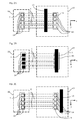
- the Fig. 1 shows schematically a test device according to the invention for electro-optical circuit boards, wherein the circuit board for the sake of clarity of drawing is not shown to scale, but enlarged.
- the printed circuit board 1 essentially consists of a substrate 2, to which electrical conductors 3 and optical waveguides 4 are applied.
- the printed circuit board 1 may have one or more complex optical and electrical layers with very many optical waveguides 4.
- the optical waveguides 4 open into cavities 5, in which a deflecting element is firmly inserted or can be temporarily used for test purposes. But you can also be led to the edge.
- the deflection element has at least one deflection mirror whose mirror surface can be shaped as desired in accordance with the respective optical requirements.
- Each optical waveguide 4 are thus associated with two deflecting mirrors, namely a deflecting mirror of a first deflecting element 6 and a deflecting mirror of a second deflecting element 7, which serve to couple 1 incident light perpendicular to the surface of the printed circuit board 1 in the optical waveguide 4 and again in the perpendicular to the surface of the Disconnect circuit board 1 extending direction.
- the test apparatus comprises a holder 8 for receiving the printed circuit board 1, a video projector 9, a camera 10 and a control device 11.
- the camera 10 and the projector 9 can be arranged stationary, but are preferably manually or controlled by corresponding motors in two parallel to Holder 8 or to the surface of the circuit board 1 extending directions, so that the beamer 9 and the camera 10 are positioned so that the beamer 9 emitted light (or light beam) by means of the deflection mirror of the two deflecting elements 6 and 7 in the optical waveguide. 4 the printed circuit board 1 einkoppelbar and in the field of view of the camera 10 can be coupled out. Such a beam path 12 is in the Fig. 1 located.
- the projector 9 is a digital projector, the composed of pixels, each pixel being a bright spot of light or black.
- the wavelength of the light projected by the projector 9 comprises the area in which the optical waveguides 4 work. That is, the projector 9 generates light in the visible and / or infrared and / or ultraviolet spectral range as needed.
- the control device 11 controls the projector 9 and the camera 10 and evaluates the measurement results.
- the control device 11 is set up to generate images with at least one first light bar and / or with at least one second light bar and / or with at least one light spot with the projector 9. At least part of the control device 11 and the projector 9 thus form a light pattern generator.
- Each of the first lightbars is characterized by a first coordinate characterizing its position within the image along a first direction and an orientation orthogonal to the first direction.
- Each of the second lightbars is characterized by a second coordinate characterizing its position within the image along a second direction and an orientation orthogonal to the second direction.
- the first and second directions are preferably orthogonal to each other.
- Each lightbar has a predetermined width and length.
- Each light spot is, for example, a bright square spot or a bright round spot of a predetermined size, although other geometries are possible.
- Each light spot is associated with a first and a second coordinate that characterize its position in the image.
- test apparatus The operation of the test apparatus will be described below with reference to an embodiment of a printed circuit board 1 having a plurality of optical fibers 4, one end of which opens into a first cavity 5 and the other end into a second cavity 5, wherein in the first cavity 5, a first deflection element. 6 and in the second cavity 5, a second deflecting element 7 is inserted.
- the projector 9 is positioned so that the projected image of him falls on the first deflecting element 6, and the camera 10 is positioned so that the second deflecting element 7 is in their field of view.
- the camera 10 thus receives images of the second deflection element 7.
- the projector 9 is used to determine for each deflection mirror of the first deflection element 6, the position that must occupy a light spot in the image projected by the projector 9, so that the light spot illuminates the deflection mirror.
- the size of the light spot is dimensioned such that, when correctly positioned within the image generated by the projector 9, it illuminates only the selected deflecting mirror, but not the adjacent deflecting mirrors.
- the projector 9 is used to selectively illuminate at least one deflection mirror with its associated light spot and to carry out the examination of the optical waveguide associated with the at least one deflection mirror. The control of the projector 9 by the control device 11 corresponding to these tasks will be explained in detail below.
- the control device 11 is set up, in the first phase A) moving a first light bar 13 projected with the projector 9 stepwise along a first direction over the first deflecting element 6 and taking an image with the camera 10 at each step, the first light bar 13 extending orthogonal to the first direction;
- the beamer 9 thus generates, controlled by the control device 11, one image after the other, wherein the first light bar 13 has a different position in each image. This position shifts along the first direction.
- Each image supplied by the camera is associated with an image of the projector 9 and thus with a first coordinate which characterizes the position of the light beam 13 along the first direction.
- the light bar 13 hits one or more deflecting mirrors 14 of the first deflecting element 6, the light is transmitted via the associated optical waveguide 4 to the associated deflecting mirror 14 of the second deflecting element 7 so that this or these deflecting mirrors 14 lights up / come on.
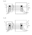
- the Fig. 2A to 2C illustrate the steps A and B.
- These figures show schematically a printed circuit board 1 with four optical fibers 4 and the two deflecting elements 6, 7, each with four deflecting mirrors 14, and the first light bar 13.
- the ends of the optical waveguide 4 and the deflecting mirror 14 are in a predetermined Spaced apart.
- the area occupied by the image of the projector 9 on the printed circuit board 1 surface is with a dashed border 15 and the field of view of the camera 10 is marked with a dashed border 16.
- the first direction is referred to here as x-direction, the second direction as y-direction.
- FIG. 2A shows a snapshot, in which the first light bar 13 is located on the one, here the left side of the deflecting mirror 14 of the first deflecting element 6 and the deflection mirror 14 is not illuminated.
- the deflecting mirror 14 of the second deflecting element 7 therefore do not light up, ie they are dark.
- the Fig. 2B shows a snapshot, in which the first light bar 13 falls on all deflecting mirrors 14 of the first deflecting element 6 and illuminates these deflecting mirror.
- the deflecting mirror 14 of the second deflecting element 7 therefore light up, ie they are bright Fig.
- FIG. 2C shows a snapshot, in which the first light bar 13 is located on the other, here the right side of the deflecting mirror 14 of the first deflecting element 6 and the deflection mirror 14 is not illuminated.
- the deflecting mirror 14 of the second deflecting element 7 therefore do not light up.
- the first set of images contains only a single image, because the first light bar 13 illuminates either all or no deflection mirror 14 of the first deflection element 6.
- the width and length of the second light bar 17 are preferably equal to the width and length of the first light bar 13.
- Each image of the beamer 9 is assigned a different position of the second light bar 17 along the second direction and thus another second coordinate of the second light bar 17.
- the Figs. 3A to 3C illustrate steps C and D.
- the Fig. 3A shows a snapshot, in which the second light bar 17 is located on the upper side of the deflection mirror 14 of the first deflecting element 6 and the deflection mirror 14 is not illuminated. The deflecting mirror 14 of the second deflecting element 7 therefore do not light up.
- the Fig. 3B shows a snapshot, in which the second light bar 17 is located above the first deflecting mirror of the first deflecting element 6 and illuminates this deflecting mirror. The first deflecting mirror of the second deflecting element 7 therefore lights up. The other deflecting mirrors are dark.
- the Fig. 3A shows a snapshot, in which the second light bar 17 is located on the upper side of the deflection mirror 14 of the first deflecting element 6 and the deflection mirror 14 is not illuminated. The deflecting mirror 14 of the second deflecting element 7 therefore do not light up.
- the Fig. 3B shows a snapshot, in which the second light
- 3C shows a snapshot, in which the second light bar 17 is located above the second deflection mirror of the first deflecting element 6 and illuminates this deflecting mirror.
- the second deflecting mirror of the second deflecting element 7 therefore lights up.
- the other deflecting mirrors are dark.
- the set of second images contains four images, since the light bar only illuminates only one deflection mirror 14 of the first deflection element 6.
- step E In the following two options for step E are explained in more detail.
- the first option is to superimpose the images of the first set of images and the images of the second set of images and to determine the intersections or crossing points where the lightbars of the images of the first set and the lightbars of the images of the second set intersect. Since the lightbars of the images of the first set are orthogonal to the first direction and the lightbars of the second set are orthogonal to the second direction, there are such intersecting points. For each intersection area or each intersection point, an image is generated for the beamer 9, which at the location of the intersection point or intersection area Light spot contains, whose size is dimensioned so that it illuminates a single deflection mirror 14, but not adjacent deflection mirror 14th
- the second possibility is to determine those first coordinates of the first lightbar 13 associated with the images of the first set of images and to determine those second coordinates of the second lightbar 17 associated with the images of the second set of images.
- the set of first images contains only a single image. There is therefore only one single first coordinate to be determined. All deflecting mirrors 14 of the first deflecting element 6 have the same x-coordinate. This first coordinate is the x-coordinate which is the first lightbar 13 in the in the Fig. 2B shown state. This first coordinate is designated x 1 .
- the second coordinates are the y coordinates that the second light bar 17 in the in the Figs. 3B and 3C shown and occupies two further states in this example.
- the pairs of coordinates characterize the positions that must occupy light spots in the image generated by the beamer 9 so that each light spot illuminates a deflection mirror 14 of the first deflection element 6 and its light is thus coupled into the optical waveguide 4 associated with the deflection mirror 14.
- there are four pairs of coordinates namely (x 1 , y 1 ), (x 1 , y 2 ), (x 1 , y 3 ) and (x 1 , y 4 ).
- the control device 11 is further set up, in the second phase F) based on the position information determined in the first phase for each optical waveguide 4 to be tested with the beamer to project a light spot 18 onto the deflection mirror 14 of the first deflection element 6 assigned to the optical waveguide 4 to be tested, the light spot 18 illuminating no deflection mirror which illuminates one is assigned to be tested optical waveguide 4 adjacent optical waveguide, take a picture with the camera 10 and to determine the quality of the optical waveguide 4 on the basis of the image.
- the FIGS. 4A and 4B illustrate this phase.
- the Fig. 4A shows the state in which a light spot 18 illuminates the first deflection mirror.
- the quality of the assigned, ie the first optical waveguide 4 is determined on the basis of the image taken by the camera 10 in this state.
- the Fig. 4B shows the state in which a light spot 18 illuminates the second deflection mirror.
- the quality of the associated, so the second optical waveguide 4 is based on the of the Camera 10 detected in this state recorded image. Etc.
- each deflecting mirror of the first deflecting element 6 can be illuminated individually, a possible cross-coupling between the optical waveguides 4 can be detected.
- cross-coupling not only the deflecting mirror of the second deflecting element 7 associated with the tested optical waveguide 4 illuminates, but also an adjacent deflecting mirror.
- the test speed can be increased if several deflection mirrors, which belong to optical waveguides 4, between which a cross coupling can be excluded for geometrical reasons, are illuminated simultaneously.
- a complex electro-optical circuit board may include a plurality of optical fibers 4, the ends of which are located at different locations, so that a plurality of cavities 5 and deflecting elements are present.
- the test apparatus can be set up so that it can perform the above-mentioned steps in parallel, both in the first phase and in the second phase, for a plurality of optical waveguides 4 insofar as the optical test is not impaired, for example by cross-coupling.
- a splitter consists of an optical fiber system with one input and two or more outputs. It can be designed in such a way that the light energy is equally distributed to the outputs. But it is also possible a different division.
- a combiner consists of an optical fiber system with two or more inputs and one output. In a splitter, a deflecting mirror of the first deflecting element 6 is illuminated on the input side and it is checked whether the brightness of the illuminating, output-side deflecting mirror corresponds to the specification. In a combiner, a deflecting mirror is illuminated on the input side after the other and checks whether the differences in the brightness of the output-side deflecting mirror do not exceed a predetermined value.
- the calibration of the test apparatus can, for example, by means of an electro-optical Reference printed circuit board whose properties were previously determined in a conventional manner.
- the Fig. 5 shows an embodiment of the test apparatus, which is suitable to test optical fibers 4 with horizontal coupling.
- the test apparatus includes at least one adapter plate 19 with resiliently mounted deflection elements 6, 7, which are automatically inserted into the cavities 5 during the test.
- the adapter plate 19 may, as also shown, also have needles 20 which contact the electrical conductors 3, so that both the electrical and the optical properties of the electro-optical circuit board 1 can be tested.
- one of the adapter plates 19 is integrated into the posture 8.
- the test device offers the advantage that the precise alignment of the light source, which generates the light spots for illuminating the deflecting mirrors, does not take place in a mechanical manner, but in terms of software by means of a beamer.
- the use of a beamer allows a precise measurement of the properties of the optical fibers without the beamer must be precisely aligned. The test time is greatly reduced.
Landscapes
- Physics & Mathematics (AREA)
- Electromagnetism (AREA)
- Engineering & Computer Science (AREA)
- Computer Networks & Wireless Communication (AREA)
- Signal Processing (AREA)
- Optics & Photonics (AREA)
- Chemical & Material Sciences (AREA)
- Analytical Chemistry (AREA)
- General Physics & Mathematics (AREA)
- Investigating Materials By The Use Of Optical Means Adapted For Particular Applications (AREA)
- Testing Of Optical Devices Or Fibers (AREA)
- Investigating Or Analysing Materials By Optical Means (AREA)
Applications Claiming Priority (1)
| Application Number | Priority Date | Filing Date | Title |
|---|---|---|---|
| CH01949/13A CH708886B1 (de) | 2013-11-22 | 2013-11-22 | Prüfvorrichtung für elektro-optische Leiterplatten. |
Publications (3)
| Publication Number | Publication Date |
|---|---|
| EP2876422A2 true EP2876422A2 (fr) | 2015-05-27 |
| EP2876422A3 EP2876422A3 (fr) | 2015-06-17 |
| EP2876422B1 EP2876422B1 (fr) | 2017-05-17 |
Family
ID=51932204
Family Applications (1)
| Application Number | Title | Priority Date | Filing Date |
|---|---|---|---|
| EP14193011.5A Active EP2876422B1 (fr) | 2013-11-22 | 2014-11-13 | Dispositif de vérification pour plaquettes électro-optiques |
Country Status (3)
| Country | Link |
|---|---|
| US (1) | US9377376B2 (fr) |
| EP (1) | EP2876422B1 (fr) |
| CH (1) | CH708886B1 (fr) |
Families Citing this family (4)
| Publication number | Priority date | Publication date | Assignee | Title |
|---|---|---|---|---|
| WO2019187073A1 (fr) * | 2018-03-30 | 2019-10-03 | 日東電工株式会社 | Procédé d'inspection de guide d'onde optique et procédé de fabrication de guide d'onde optique faisant appel audit procédé |
| US11499923B2 (en) * | 2020-09-30 | 2022-11-15 | Openlight Photonics, Inc. | On-chip photonic integrated circuit optical validation |
| EP4012511B1 (fr) * | 2020-12-11 | 2023-08-23 | Montres Breguet S.A. | Procede d'accordage harmonique d'au moins un timbre d'un mecanisme de sonnerie d'une montre |
| CN114397091A (zh) * | 2021-12-07 | 2022-04-26 | 伟创力电子技术(苏州)有限公司 | 一种光波导模组的自动测试方法 |
Family Cites Families (6)
| Publication number | Priority date | Publication date | Assignee | Title |
|---|---|---|---|---|
| GB2082012A (en) * | 1980-06-20 | 1982-02-24 | Light Optics Ltd | Non-coherent fibre-optic bundle image decoder |
| GB2128839A (en) * | 1982-10-15 | 1984-05-02 | Dainichi Nippon Cables Ltd | Image display apparatus |
| US6678437B2 (en) * | 2001-03-30 | 2004-01-13 | Analog Devices, Inc. | Method of and architecture for optically switching light communication signals in fiber optic networks and the like |
| US20040091200A1 (en) * | 2002-11-13 | 2004-05-13 | Olympus Optical Co., Ltd. | Optical switch device |
| US7050670B2 (en) * | 2003-08-07 | 2006-05-23 | Avago Technologies | Method and system for aligning and maintaining alignment of an optical switch using sensors |
| US20110013905A1 (en) * | 2009-07-17 | 2011-01-20 | Avago Technologies Fiber Ip (Singapore) Pte. Ltd. | Active optical cable apparatus and method for detecting optical fiber breakage |
-
2013
- 2013-11-22 CH CH01949/13A patent/CH708886B1/de not_active IP Right Cessation
-
2014
- 2014-11-13 EP EP14193011.5A patent/EP2876422B1/fr active Active
- 2014-11-21 US US14/550,693 patent/US9377376B2/en active Active
Non-Patent Citations (1)
| Title |
|---|
| None |
Also Published As
| Publication number | Publication date |
|---|---|
| EP2876422B1 (fr) | 2017-05-17 |
| US9377376B2 (en) | 2016-06-28 |
| CH708886B1 (de) | 2017-06-30 |
| CH708886A2 (de) | 2015-05-29 |
| EP2876422A3 (fr) | 2015-06-17 |
| US20150146195A1 (en) | 2015-05-28 |
Similar Documents
| Publication | Publication Date | Title |
|---|---|---|
| DE69412281T2 (de) | Ausrichtsysteme | |
| DE69832940T2 (de) | Beobachtungsgerät und Gerät zum Verschmelzungsspleissen von optischen Fasern | |
| DE69522524T2 (de) | Verfahren zum Spleissen von polarisationserhaltenden Glasfasern | |
| DE2802417C2 (fr) | ||
| EP3076148A1 (fr) | Dispositif et procédé de mesure de caractéristiques d'imagerie d'un système d'imagerie optique | |
| DE69816098T2 (de) | System zur visualisierung und bilderzeugung | |
| CH488202A (de) | Verfahren und Vorrichtung zur automatischen Scharfeinstellung optischer Systeme | |
| DE112011100269T5 (de) | Leiterplattenprüfvorrichtung | |
| DE69407078T2 (de) | Bildprojektionsapparat mit Autofokus-System | |
| EP2876422B1 (fr) | Dispositif de vérification pour plaquettes électro-optiques | |
| DE102014108386A1 (de) | Optisches System und Verfahren | |
| EP3147700B1 (fr) | Procede et dispositif d'agrandissement du champ de vision d'une camera et camera en etant equipee | |
| DE102011001785A1 (de) | Belichtungseinrichtung zur strukturierten Belichtung einer Fläche | |
| DE10014334C2 (de) | Vorrichtung und Verfahren zur ortsaufgelösten Brechkraft-Bestimmung | |
| DE4301546C2 (de) | Einrichtung zum Prüfen von Oberflächen von Werkstücken | |
| DE3924951A1 (de) | Verfahren und vorrichtung zum ausrichten von bildsensoren auf ein optisches system eines optischen geraetes | |
| DE102015103254A1 (de) | Optisches System | |
| WO2008046494A1 (fr) | système d'éclairage | |
| DE3248382A1 (de) | Verfahren und vorrichtung zum ausrichten | |
| EP3086151A1 (fr) | Systeme et procede d'alignement d'un ecran par rapport a un axe optique | |
| DE102007063453B3 (de) | Anordnung zur automatischen optischen Inspektion von bestückten Leiterplatten | |
| DE102019133738A1 (de) | Vorrichtung, Verfahren und Verwendung der Vorrichtung zur Justage, Montage und/oder Prüfung eines elektrooptischen Systems | |
| DE4214968C2 (de) | Vorrichtung zur Bilderkennung | |
| DE102019108124A1 (de) | Verfahren und Vorrichtung zur interferometrischen Schwingungsmessung an einer Mehrzahl von Messpunkten mittels eines Messlaserstrahls | |
| DE3709500A1 (de) | Optische bahnueberwachungseinrichtung mit zeilenkameras mit gerichteter beleuchtung |
Legal Events
| Date | Code | Title | Description |
|---|---|---|---|
| PUAL | Search report despatched |
Free format text: ORIGINAL CODE: 0009013 |
|
| PUAI | Public reference made under article 153(3) epc to a published international application that has entered the european phase |
Free format text: ORIGINAL CODE: 0009012 |
|
| 17P | Request for examination filed |
Effective date: 20141113 |
|
| AK | Designated contracting states |
Kind code of ref document: A2 Designated state(s): AL AT BE BG CH CY CZ DE DK EE ES FI FR GB GR HR HU IE IS IT LI LT LU LV MC MK MT NL NO PL PT RO RS SE SI SK SM TR |
|
| AX | Request for extension of the european patent |
Extension state: BA ME |
|
| AK | Designated contracting states |
Kind code of ref document: A3 Designated state(s): AL AT BE BG CH CY CZ DE DK EE ES FI FR GB GR HR HU IE IS IT LI LT LU LV MC MK MT NL NO PL PT RO RS SE SI SK SM TR |
|
| AX | Request for extension of the european patent |
Extension state: BA ME |
|
| RIC1 | Information provided on ipc code assigned before grant |
Ipc: G01M 11/00 20060101AFI20150512BHEP |
|
| R17P | Request for examination filed (corrected) |
Effective date: 20150814 |
|
| RBV | Designated contracting states (corrected) |
Designated state(s): AL AT BE BG CH CY CZ DE DK EE ES FI FR GB GR HR HU IE IS IT LI LT LU LV MC MK MT NL NO PL PT RO RS SE SI SK SM TR |
|
| GRAP | Despatch of communication of intention to grant a patent |
Free format text: ORIGINAL CODE: EPIDOSNIGR1 |
|
| STAA | Information on the status of an ep patent application or granted ep patent |
Free format text: STATUS: GRANT OF PATENT IS INTENDED |
|
| GRAS | Grant fee paid |
Free format text: ORIGINAL CODE: EPIDOSNIGR3 |
|
| INTG | Intention to grant announced |
Effective date: 20170315 |
|
| GRAA | (expected) grant |
Free format text: ORIGINAL CODE: 0009210 |
|
| STAA | Information on the status of an ep patent application or granted ep patent |
Free format text: STATUS: THE PATENT HAS BEEN GRANTED |
|
| AK | Designated contracting states |
Kind code of ref document: B1 Designated state(s): AL AT BE BG CH CY CZ DE DK EE ES FI FR GB GR HR HU IE IS IT LI LT LU LV MC MK MT NL NO PL PT RO RS SE SI SK SM TR |
|
| REG | Reference to a national code |
Ref country code: GB Ref legal event code: FG4D Free format text: NOT ENGLISH |
|
| REG | Reference to a national code |
Ref country code: CH Ref legal event code: EP Ref country code: CH Ref legal event code: NV Representative=s name: PATENTANWALTSBUERO DR. URS FALK, CH |
|
| REG | Reference to a national code |
Ref country code: IE Ref legal event code: FG4D Free format text: LANGUAGE OF EP DOCUMENT: GERMAN |
|
| REG | Reference to a national code |
Ref country code: AT Ref legal event code: REF Ref document number: 894899 Country of ref document: AT Kind code of ref document: T Effective date: 20170615 |
|
| REG | Reference to a national code |
Ref country code: DE Ref legal event code: R096 Ref document number: 502014003853 Country of ref document: DE |
|
| REG | Reference to a national code |
Ref country code: NL Ref legal event code: MP Effective date: 20170517 |
|
| REG | Reference to a national code |
Ref country code: LT Ref legal event code: MG4D |
|
| PG25 | Lapsed in a contracting state [announced via postgrant information from national office to epo] |
Ref country code: LT Free format text: LAPSE BECAUSE OF FAILURE TO SUBMIT A TRANSLATION OF THE DESCRIPTION OR TO PAY THE FEE WITHIN THE PRESCRIBED TIME-LIMIT Effective date: 20170517 Ref country code: FI Free format text: LAPSE BECAUSE OF FAILURE TO SUBMIT A TRANSLATION OF THE DESCRIPTION OR TO PAY THE FEE WITHIN THE PRESCRIBED TIME-LIMIT Effective date: 20170517 Ref country code: GR Free format text: LAPSE BECAUSE OF FAILURE TO SUBMIT A TRANSLATION OF THE DESCRIPTION OR TO PAY THE FEE WITHIN THE PRESCRIBED TIME-LIMIT Effective date: 20170818 Ref country code: ES Free format text: LAPSE BECAUSE OF FAILURE TO SUBMIT A TRANSLATION OF THE DESCRIPTION OR TO PAY THE FEE WITHIN THE PRESCRIBED TIME-LIMIT Effective date: 20170517 Ref country code: NO Free format text: LAPSE BECAUSE OF FAILURE TO SUBMIT A TRANSLATION OF THE DESCRIPTION OR TO PAY THE FEE WITHIN THE PRESCRIBED TIME-LIMIT Effective date: 20170817 Ref country code: HR Free format text: LAPSE BECAUSE OF FAILURE TO SUBMIT A TRANSLATION OF THE DESCRIPTION OR TO PAY THE FEE WITHIN THE PRESCRIBED TIME-LIMIT Effective date: 20170517 |
|
| REG | Reference to a national code |
Ref country code: FR Ref legal event code: PLFP Year of fee payment: 4 |
|
| PG25 | Lapsed in a contracting state [announced via postgrant information from national office to epo] |
Ref country code: PL Free format text: LAPSE BECAUSE OF FAILURE TO SUBMIT A TRANSLATION OF THE DESCRIPTION OR TO PAY THE FEE WITHIN THE PRESCRIBED TIME-LIMIT Effective date: 20170517 Ref country code: RS Free format text: LAPSE BECAUSE OF FAILURE TO SUBMIT A TRANSLATION OF THE DESCRIPTION OR TO PAY THE FEE WITHIN THE PRESCRIBED TIME-LIMIT Effective date: 20170517 Ref country code: NL Free format text: LAPSE BECAUSE OF FAILURE TO SUBMIT A TRANSLATION OF THE DESCRIPTION OR TO PAY THE FEE WITHIN THE PRESCRIBED TIME-LIMIT Effective date: 20170517 Ref country code: SE Free format text: LAPSE BECAUSE OF FAILURE TO SUBMIT A TRANSLATION OF THE DESCRIPTION OR TO PAY THE FEE WITHIN THE PRESCRIBED TIME-LIMIT Effective date: 20170517 Ref country code: LV Free format text: LAPSE BECAUSE OF FAILURE TO SUBMIT A TRANSLATION OF THE DESCRIPTION OR TO PAY THE FEE WITHIN THE PRESCRIBED TIME-LIMIT Effective date: 20170517 Ref country code: IS Free format text: LAPSE BECAUSE OF FAILURE TO SUBMIT A TRANSLATION OF THE DESCRIPTION OR TO PAY THE FEE WITHIN THE PRESCRIBED TIME-LIMIT Effective date: 20170917 Ref country code: BG Free format text: LAPSE BECAUSE OF FAILURE TO SUBMIT A TRANSLATION OF THE DESCRIPTION OR TO PAY THE FEE WITHIN THE PRESCRIBED TIME-LIMIT Effective date: 20170817 |
|
| PG25 | Lapsed in a contracting state [announced via postgrant information from national office to epo] |
Ref country code: CZ Free format text: LAPSE BECAUSE OF FAILURE TO SUBMIT A TRANSLATION OF THE DESCRIPTION OR TO PAY THE FEE WITHIN THE PRESCRIBED TIME-LIMIT Effective date: 20170517 Ref country code: SK Free format text: LAPSE BECAUSE OF FAILURE TO SUBMIT A TRANSLATION OF THE DESCRIPTION OR TO PAY THE FEE WITHIN THE PRESCRIBED TIME-LIMIT Effective date: 20170517 Ref country code: DK Free format text: LAPSE BECAUSE OF FAILURE TO SUBMIT A TRANSLATION OF THE DESCRIPTION OR TO PAY THE FEE WITHIN THE PRESCRIBED TIME-LIMIT Effective date: 20170517 Ref country code: RO Free format text: LAPSE BECAUSE OF FAILURE TO SUBMIT A TRANSLATION OF THE DESCRIPTION OR TO PAY THE FEE WITHIN THE PRESCRIBED TIME-LIMIT Effective date: 20170517 Ref country code: EE Free format text: LAPSE BECAUSE OF FAILURE TO SUBMIT A TRANSLATION OF THE DESCRIPTION OR TO PAY THE FEE WITHIN THE PRESCRIBED TIME-LIMIT Effective date: 20170517 |
|
| REG | Reference to a national code |
Ref country code: DE Ref legal event code: R097 Ref document number: 502014003853 Country of ref document: DE |
|
| PG25 | Lapsed in a contracting state [announced via postgrant information from national office to epo] |
Ref country code: IT Free format text: LAPSE BECAUSE OF FAILURE TO SUBMIT A TRANSLATION OF THE DESCRIPTION OR TO PAY THE FEE WITHIN THE PRESCRIBED TIME-LIMIT Effective date: 20170517 Ref country code: SM Free format text: LAPSE BECAUSE OF FAILURE TO SUBMIT A TRANSLATION OF THE DESCRIPTION OR TO PAY THE FEE WITHIN THE PRESCRIBED TIME-LIMIT Effective date: 20170517 |
|
| PLBE | No opposition filed within time limit |
Free format text: ORIGINAL CODE: 0009261 |
|
| STAA | Information on the status of an ep patent application or granted ep patent |
Free format text: STATUS: NO OPPOSITION FILED WITHIN TIME LIMIT |
|
| 26N | No opposition filed |
Effective date: 20180220 |
|
| PG25 | Lapsed in a contracting state [announced via postgrant information from national office to epo] |
Ref country code: SI Free format text: LAPSE BECAUSE OF FAILURE TO SUBMIT A TRANSLATION OF THE DESCRIPTION OR TO PAY THE FEE WITHIN THE PRESCRIBED TIME-LIMIT Effective date: 20170517 |
|
| PG25 | Lapsed in a contracting state [announced via postgrant information from national office to epo] |
Ref country code: MC Free format text: LAPSE BECAUSE OF FAILURE TO SUBMIT A TRANSLATION OF THE DESCRIPTION OR TO PAY THE FEE WITHIN THE PRESCRIBED TIME-LIMIT Effective date: 20170517 |
|
| PG25 | Lapsed in a contracting state [announced via postgrant information from national office to epo] |
Ref country code: LU Free format text: LAPSE BECAUSE OF NON-PAYMENT OF DUE FEES Effective date: 20171113 |
|
| REG | Reference to a national code |
Ref country code: IE Ref legal event code: MM4A |
|
| PG25 | Lapsed in a contracting state [announced via postgrant information from national office to epo] |
Ref country code: MT Free format text: LAPSE BECAUSE OF FAILURE TO SUBMIT A TRANSLATION OF THE DESCRIPTION OR TO PAY THE FEE WITHIN THE PRESCRIBED TIME-LIMIT Effective date: 20170517 |
|
| PG25 | Lapsed in a contracting state [announced via postgrant information from national office to epo] |
Ref country code: IE Free format text: LAPSE BECAUSE OF NON-PAYMENT OF DUE FEES Effective date: 20171113 |
|
| PG25 | Lapsed in a contracting state [announced via postgrant information from national office to epo] |
Ref country code: HU Free format text: LAPSE BECAUSE OF FAILURE TO SUBMIT A TRANSLATION OF THE DESCRIPTION OR TO PAY THE FEE WITHIN THE PRESCRIBED TIME-LIMIT; INVALID AB INITIO Effective date: 20141113 |
|
| PG25 | Lapsed in a contracting state [announced via postgrant information from national office to epo] |
Ref country code: CY Free format text: LAPSE BECAUSE OF FAILURE TO SUBMIT A TRANSLATION OF THE DESCRIPTION OR TO PAY THE FEE WITHIN THE PRESCRIBED TIME-LIMIT Effective date: 20170517 |
|
| PG25 | Lapsed in a contracting state [announced via postgrant information from national office to epo] |
Ref country code: MK Free format text: LAPSE BECAUSE OF FAILURE TO SUBMIT A TRANSLATION OF THE DESCRIPTION OR TO PAY THE FEE WITHIN THE PRESCRIBED TIME-LIMIT Effective date: 20170517 |
|
| PG25 | Lapsed in a contracting state [announced via postgrant information from national office to epo] |
Ref country code: TR Free format text: LAPSE BECAUSE OF FAILURE TO SUBMIT A TRANSLATION OF THE DESCRIPTION OR TO PAY THE FEE WITHIN THE PRESCRIBED TIME-LIMIT Effective date: 20170517 |
|
| PG25 | Lapsed in a contracting state [announced via postgrant information from national office to epo] |
Ref country code: PT Free format text: LAPSE BECAUSE OF FAILURE TO SUBMIT A TRANSLATION OF THE DESCRIPTION OR TO PAY THE FEE WITHIN THE PRESCRIBED TIME-LIMIT Effective date: 20170517 |
|
| PG25 | Lapsed in a contracting state [announced via postgrant information from national office to epo] |
Ref country code: AL Free format text: LAPSE BECAUSE OF FAILURE TO SUBMIT A TRANSLATION OF THE DESCRIPTION OR TO PAY THE FEE WITHIN THE PRESCRIBED TIME-LIMIT Effective date: 20170517 |
|
| REG | Reference to a national code |
Ref country code: AT Ref legal event code: MM01 Ref document number: 894899 Country of ref document: AT Kind code of ref document: T Effective date: 20191113 |
|
| PG25 | Lapsed in a contracting state [announced via postgrant information from national office to epo] |
Ref country code: AT Free format text: LAPSE BECAUSE OF NON-PAYMENT OF DUE FEES Effective date: 20191113 |
|
| PGFP | Annual fee paid to national office [announced via postgrant information from national office to epo] |
Ref country code: GB Payment date: 20250925 Year of fee payment: 12 |
|
| PGFP | Annual fee paid to national office [announced via postgrant information from national office to epo] |
Ref country code: FR Payment date: 20250922 Year of fee payment: 12 |
|
| REG | Reference to a national code |
Ref country code: CH Ref legal event code: U11 Free format text: ST27 STATUS EVENT CODE: U-0-0-U10-U11 (AS PROVIDED BY THE NATIONAL OFFICE) Effective date: 20251201 |
|
| PGFP | Annual fee paid to national office [announced via postgrant information from national office to epo] |
Ref country code: DE Payment date: 20250916 Year of fee payment: 12 |
|
| PGFP | Annual fee paid to national office [announced via postgrant information from national office to epo] |
Ref country code: BE Payment date: 20251003 Year of fee payment: 12 |
|
| PGFP | Annual fee paid to national office [announced via postgrant information from national office to epo] |
Ref country code: CH Payment date: 20251201 Year of fee payment: 12 |