EP2876494A1 - Modulateur électro-optique - Google Patents
Modulateur électro-optique Download PDFInfo
- Publication number
- EP2876494A1 EP2876494A1 EP13194250.0A EP13194250A EP2876494A1 EP 2876494 A1 EP2876494 A1 EP 2876494A1 EP 13194250 A EP13194250 A EP 13194250A EP 2876494 A1 EP2876494 A1 EP 2876494A1
- Authority
- EP
- European Patent Office
- Prior art keywords
- electro
- optical modulator
- electrode arrangement
- terminating resistors
- modulator
- Prior art date
- Legal status (The legal status is an assumption and is not a legal conclusion. Google has not performed a legal analysis and makes no representation as to the accuracy of the status listed.)
- Granted
Links
Images


Classifications
-
- G—PHYSICS
- G02—OPTICS
- G02F—OPTICAL DEVICES OR ARRANGEMENTS FOR THE CONTROL OF LIGHT BY MODIFICATION OF THE OPTICAL PROPERTIES OF THE MEDIA OF THE ELEMENTS INVOLVED THEREIN; NON-LINEAR OPTICS; FREQUENCY-CHANGING OF LIGHT; OPTICAL LOGIC ELEMENTS; OPTICAL ANALOGUE/DIGITAL CONVERTERS
- G02F1/00—Devices or arrangements for the control of the intensity, colour, phase, polarisation or direction of light arriving from an independent light source, e.g. switching, gating or modulating; Non-linear optics
- G02F1/01—Devices or arrangements for the control of the intensity, colour, phase, polarisation or direction of light arriving from an independent light source, e.g. switching, gating or modulating; Non-linear optics for the control of the intensity, phase, polarisation or colour
- G02F1/21—Devices or arrangements for the control of the intensity, colour, phase, polarisation or direction of light arriving from an independent light source, e.g. switching, gating or modulating; Non-linear optics for the control of the intensity, phase, polarisation or colour by interference
- G02F1/225—Devices or arrangements for the control of the intensity, colour, phase, polarisation or direction of light arriving from an independent light source, e.g. switching, gating or modulating; Non-linear optics for the control of the intensity, phase, polarisation or colour by interference in an optical waveguide structure
- G02F1/2255—Devices or arrangements for the control of the intensity, colour, phase, polarisation or direction of light arriving from an independent light source, e.g. switching, gating or modulating; Non-linear optics for the control of the intensity, phase, polarisation or colour by interference in an optical waveguide structure controlled by a high-frequency electromagnetic component in an electric waveguide structure
-
- G—PHYSICS
- G02—OPTICS
- G02F—OPTICAL DEVICES OR ARRANGEMENTS FOR THE CONTROL OF LIGHT BY MODIFICATION OF THE OPTICAL PROPERTIES OF THE MEDIA OF THE ELEMENTS INVOLVED THEREIN; NON-LINEAR OPTICS; FREQUENCY-CHANGING OF LIGHT; OPTICAL LOGIC ELEMENTS; OPTICAL ANALOGUE/DIGITAL CONVERTERS
- G02F1/00—Devices or arrangements for the control of the intensity, colour, phase, polarisation or direction of light arriving from an independent light source, e.g. switching, gating or modulating; Non-linear optics
- G02F1/01—Devices or arrangements for the control of the intensity, colour, phase, polarisation or direction of light arriving from an independent light source, e.g. switching, gating or modulating; Non-linear optics for the control of the intensity, phase, polarisation or colour
- G02F1/21—Devices or arrangements for the control of the intensity, colour, phase, polarisation or direction of light arriving from an independent light source, e.g. switching, gating or modulating; Non-linear optics for the control of the intensity, phase, polarisation or colour by interference
- G02F1/225—Devices or arrangements for the control of the intensity, colour, phase, polarisation or direction of light arriving from an independent light source, e.g. switching, gating or modulating; Non-linear optics for the control of the intensity, phase, polarisation or colour by interference in an optical waveguide structure
- G02F1/2257—Devices or arrangements for the control of the intensity, colour, phase, polarisation or direction of light arriving from an independent light source, e.g. switching, gating or modulating; Non-linear optics for the control of the intensity, phase, polarisation or colour by interference in an optical waveguide structure the optical waveguides being made of semiconducting material
-
- G—PHYSICS
- G02—OPTICS
- G02F—OPTICAL DEVICES OR ARRANGEMENTS FOR THE CONTROL OF LIGHT BY MODIFICATION OF THE OPTICAL PROPERTIES OF THE MEDIA OF THE ELEMENTS INVOLVED THEREIN; NON-LINEAR OPTICS; FREQUENCY-CHANGING OF LIGHT; OPTICAL LOGIC ELEMENTS; OPTICAL ANALOGUE/DIGITAL CONVERTERS
- G02F1/00—Devices or arrangements for the control of the intensity, colour, phase, polarisation or direction of light arriving from an independent light source, e.g. switching, gating or modulating; Non-linear optics
- G02F1/01—Devices or arrangements for the control of the intensity, colour, phase, polarisation or direction of light arriving from an independent light source, e.g. switching, gating or modulating; Non-linear optics for the control of the intensity, phase, polarisation or colour
- G02F1/21—Devices or arrangements for the control of the intensity, colour, phase, polarisation or direction of light arriving from an independent light source, e.g. switching, gating or modulating; Non-linear optics for the control of the intensity, phase, polarisation or colour by interference
- G02F1/212—Mach-Zehnder type
-
- G—PHYSICS
- G02—OPTICS
- G02F—OPTICAL DEVICES OR ARRANGEMENTS FOR THE CONTROL OF LIGHT BY MODIFICATION OF THE OPTICAL PROPERTIES OF THE MEDIA OF THE ELEMENTS INVOLVED THEREIN; NON-LINEAR OPTICS; FREQUENCY-CHANGING OF LIGHT; OPTICAL LOGIC ELEMENTS; OPTICAL ANALOGUE/DIGITAL CONVERTERS
- G02F2201/00—Constructional arrangements not provided for in groups G02F1/00 - G02F7/00
- G02F2201/12—Constructional arrangements not provided for in groups G02F1/00 - G02F7/00 electrode
- G02F2201/127—Constructional arrangements not provided for in groups G02F1/00 - G02F7/00 electrode travelling wave
Definitions
- the invention relates to an electro-optical modulator according to the preamble of claim 1.
- Such electro-optical modulators comprise, for example, a high frequency electrode arrangement used for supplying a voltage across optical waveguides of the modulators for creating a phase shift of the optical waves propagating in the waveguides.
- travelling wave electrodes are used for supplying a voltage to the optical modulator waveguides as disclosed in the publication " High-Speed III-V Semiconductor Intensity Modulators", Robert G. Walker, IEEE Journal of Quantum Electronics Vol. 27, No. 3, March 1991 .
- These known modulators tend be rather large if pre-determined electrical power losses shall not be exceeded.
- an electro-optical modulator comprising
- the design of the capacitive structure in particular permits a rather compact layout of the electro-optical modulator and at the same time allows the modulator to be driven by a driver unit (i.e. an amplifier) in open collector configuration to keep power losses low.
- a driver unit i.e. an amplifier
- the driver unit e.g. a driver chip
- the first and second electrical line, the terminating resistors and the (blocking) capacitive structure of the modulator can be regarded as integral components of the open collector circuitry (e.g. a high frequency open collector circuitry) as will be explained in more detail below.
- an immersive electrical design of the driver unit and the electrical lines and the terminating network (comprising the terminating resistors and the capacitive structure) of the modulator will be carried out in particular to adapt the overall impedance of these components and thus to optimize the performance of the modulator.
- modulator devices i.e. the combination of the driver unit and the modulator
- modulator devices employed e.g. for long-distance applications, having power losses smaller than 400 mW may be realized.
- compact high frequency modulator modules having e.g. a transmission rate of at least 100 Gbit/s
- the galvanic separation of the terminating resistors by means of the capacitive structure permits to apply different (DC) bias voltages to the first and the second electrical line, respectively.
- the capacitive structure and the first and second electrical line of the electrode arrangement are arranged on a common substrate, i.e. the capacitive structure and the electrical lines are monolithically integrated.
- the terminating resistors and the first and second electrical line may be arranged on a common substrate, wherein, in particular, the capacitive structure, the terminating resistors and the electrical lines are monolithically integrated, i.e. these components are arranged on the same substrate and e.g. are fabricated using the same semiconductor technology.
- the terminating resistors each may be formed by a material layer (i.e. as a planar structure) or a plurality of material layers, which may result in an enhanced scalability of the terminating resistors.
- bond connections between the terminating resistors and/or the capacitive structure and the electrical lines via bonding wires are not required such that e.g. adapting the impedance of the network formed by the electrode arrangement, the terminating resistors and or the capacitive structure is facilitated.
- the possibility of precise impedance matching may be important in particular if this network forms part of an integral open collector circuitry as set forth above.
- the monolithic design of the modulator may facilitate the integration of a plurality of modulators into a module.
- the terminating resistors and/or the capacitive structure may also be formed as separate components arranged e.g. on a different substrate (e.g. a ceramic substrate) than the electrical lines of the electrode arrangement and/or coupled to the first and the second electrical line of the modulator, e.g. via bonding wires.
- a different substrate e.g. a ceramic substrate
- the first one of the conductive layers is connected to a first one of the terminating resistors and a second one of the conductive layers is connected to a second one of the terminating resistors.
- This configuration in particular allows the modulator to be part of an open collector circuit, wherein the two terminating resistors are coupled via a single capacitance formed by the conductive layers and the dielectric layer in between.
- the capacitive structure comprises three electrically conductive layers and at least one dielectric layer to form two capacitors via which the first and the second terminating resistor is connected to ground, thereby forming a part of another open collector circuit as will be discussed in more detail below. More particularly, a first and a third one of the conductive layers are separated by the dielectric layer and a second one of the conductive layers and the third conductive layer are separated by the dielectric layer, and wherein the first conductive layer is connected to a first one of the terminating resistors, the second conductive layer is connected to a second one of terminating resistors, and wherein the third conductive layer is grounded.
- the first and the second electrical line of the electrode arrangement may form a coplanar strip line.
- the coplanar strip line is operated as a travelling wave electrode, e.g. of a Mach-Zehnder modulator.
- the first and the second electrical line may be capacitively coupled to one another, i.e. a capacitor or a plurality of capacitors may be provided via which the first electrical line is coupled to the second electrical line.
- the modulator according to the invention is a capacitively loaded Mach-Zehnder modulator, wherein the first and the second electrical line form the two planar lines of a travelling wave coplanar line.
- such a modulator may also be operated as a phase modulator, wherein only one of the two optical waveguides of the modulator is used to modulate the phase of an optical signal.
- the one of the optical waveguides that is not used may be optically inactive, wherein, however, capacitive segments formed by the optically inactive waveguide are used for capacitively coupling of waveguide electrodes arranged on top of the optically active waveguide to the driver unit.
- the first and the second electrical line may extend in a first distance from one another, wherein in a second region of the electrode arrangement the first and the second electrical line extend in a second distance from one another that is larger than the first distance, wherein the two terminating resistors are arranged between the first and the second electrical line in the second region of the electrode arrangement.
- the two terminating resistors in particular are arranged in a distance from the optical waveguides of the modulator (but e.g. symmetrically with respect to the optical waveguides) in order to reduce the thermal impact on the waveguides. The greater the required distance from the optical waveguides, the more the distance between the first and the second electrical has to be increased.
- the capacitive structure may be used for adapting the impedance of the electrode arrangement.
- the conductive structure may influence the effective distance of the first and a second electrical line, i.e. the distance between the first and a second electrical line that determines the impedance of the electrode arrangement (e.g. forming a coplanar strip line as mentioned above).
- the capacitive structure may be arranged at least partially between the first and the second electrical line in a widened region of the electrode arrangement, i.e. in the second region of the electrode arrangement as set forth above.
- the geometry of the capacitive structure is chosen in such a way that the effective distance of the widened second region of the electrode arrangement and thus the impedance of the electrode arrangement (i.e. the impedance of the first and the second optical line) at least essentially equals the impedance of straight first and second electrical lines (e.g. a straight coplanar strip line), i.e. an electrode arrangement whose first and second electrical line are disposed in the first distance from one another over their entire length.
- straight first and second electrical lines e.g. a straight coplanar strip line
- the first and a second electrical line may be driven symmetrically ("differential drive"), i.e. the driver unit may be configured for supplying a differential voltage signal to the flexible coplanar strip and thus to the coplanar strip line of the modulator.
- the driver unit may be configured for supplying a differential voltage signal to the flexible coplanar strip and thus to the coplanar strip line of the modulator.
- none of the electrical lines of the electrode arrangement and/or of the flexible coplanar strip line is grounded.
- the first and the second electrical line may also be formed as geometrically symmetric structures.
- the modulator according to the invention comprises two optical waveguides (see above), wherein the terminating resistors are arranged symmetrically with respect to the optical waveguides.
- the electro-optical modulator according to the invention may comprise a driver unit supplying a differential voltage signal to the electrode arrangement. Examples of symmetrically driven electrodes are disclosed in the European patent applications EP 2 615 489 and EP 2 615 490 which in that respect are enclosed by reference herewith
- the driver unit is operated in open collector mode or in open collector mode with back termination.
- the driver unit may be operated in open drain or in open drain mode with back termination (if the driver unit is a CMOS device).
- the driver unit may have an internal terminating resistance that equals the impedance of the electrode arrangement, wherein the impedance of the first and the second electrical line and other electrical components (such as the terminating resistor mentioned above) is matched to the internal terminating resistance of the driver unit.
- the driver unit may supply a differential voltage to the coplanar strip line of the modulator as also already mentioned above.
- the modulator comprises an additional capacitor having a larger capacitance than the capacitive structure, wherein the two terminating resistors are coupled to one another via the capacitive structure and the additional capacitor.
- the capacitance e.g. 10-80 pF, in particular 20-30 pF
- the additional capacitor permits the terminating resistors to be capacitively coupled also with respect to lower frequencies.
- the modulator according to the invention may be realized using indium phosphide technology, i.e. components of the modulator such as the electrode arrangement and optical waveguides are arranged on an indium phosphide substrate.
- the modulator can be fabricating using other technologies, i.e. substrates and semiconductor layers based on other materials such as gallium arsenide or silicon.
- FIGS 1A to 1C illustrate a detail of an electrode arrangement 1 of an electro-optical travelling wave modulator according to an embodiment of the invention.
- the electrode arrangement 1 comprises a first and a second electrical line 11, 12 forming a coplanar strip line.
- the electrical lines 11, 12 are connected to waveguide electrodes 113, 123 via air bridges 111, 121 for applying a voltage across optical waveguides 112, 122 of the modulator as in principle known from the prior art.
- the first and the second waveguide electrodes 113, 123 are arranged on top of first and second capacitive segments 114, 124 of the optical wave guides 112, 122 such that the first and the second waveguide electrodes 113, 123 and thus the first and second electrical lines 11, 12 are capacitively coupled to one another.
- two terminating resistors 21, 22 are arranged between the electrical lines 11, 12, wherein the terminating resistors 21, 22 are formed as material layers arranged on a substrate together with the coplanar strip line, i.e. the terminating resistors 21, 22 are monolithically integrated with other components of the electro-optic modulator.
- the gap between the electrical lines 11, 12 widens towards the terminating resistors 21, 22 such that the electrode arrangement 1 comprises a first section 10 in which the electrical lines 11, 12 extend with a first distance from one another and a second region 20 in which the electrical lines 21, 22 extend with a second distance from one another, wherein the second distance is larger than the first distance.
- the second distance may be chosen to allow the terminating resistors 21, 22 to be arranged in such a way that thermal impact of the resistors 21, 22 on the optical wave guides 112, 122 are kept as low as possible.
- the distance between the electrical lines 11, 12 in the second region 20 is at least 50 ⁇ m.
- a capacitive structure in the form of a metal structure 31 is arranged in the second region 20 of the electrode arrangement 1 between the electrical lines 11, 12 forming a capacitive structure that galvanically separates the two terminating resistors 21, 22.
- the metal structure 31 comprises two metal layers 313, 314 arranged one above the other (see Figure 1 C) , wherein the metal layers 313, 314 (e.g. gold layers) are separated by a dielectric layer 315 (e.g. a silicon nitride or a silicon oxide layer) arranged between them.
- the upper metal layer 313 is electrically connected to the first terminating resistor 21, wherein the lower metal layer 314 is electrically connected to the second terminating resistor 22.
- the metal structure 31 provides a capacitor coupling the two terminating resistors 21, 22.
- the capacitive coupling between the two terminating resistors 21, 22 provided by the metal structure 31 can be used to realize an open collector circuit shown in Figure 3 .
- the metal structure 31 may be configured in such a way that the influence of the larger distance between the electrical lines 11, 12 in the second region 20 on the impedance of the coplanar strip line is compensated.
- the metal structure 31 reduces the effective distance between the first and the second electrical line 11, 12, which determines the impedance of the coplanar strip-line, such that a deteriorating effect of the increased distance between the electrical lines 11, 12 in the region of the terminating resistors 21, 22 may be counteracted.
- the dimensions of the metal structure 31 are chosen in such a way that the impedance of the coplanar strip line formed by the electrical lines 11, 12 is adapted to the desired overall impedance of the coplanar line.
- the effective distance of the electrical lines 11, 12 from one another varies with the geometry of the metal structure 31 such that the metal structure 31 can be used to adapt the impedance of the coplanar strip line.
- Figure 2 illustrates a modification of the design of the metal structure 31, the metal structure according to this embodiment having three metal layers 313, 314 and 316.
- the first metal layer 313 is galvanically isolated from the third (middle) metal layer 316 by a first dielectric layer 317 and the second metal layer 314 is galvanically isolated from the third metal layer 316 by a second dielectric layer 318, thereby forming a first and a second capacitor.
- a single dielectric layer embedding the middle metal layer 316 could be arranged.
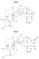
- the middle metal layer 316 will be grounded, wherein the first, upper metal layer 313 is connected to the first terminating resistor 21 and the second, lower metal layer 314 is connected to the second terminating resistor 22 to realize the alternative open collector circuitry shown in Figure 4 . That is, the termination of the coplanar strip line is not realized by a single capacitor, but by two capacitors, wherein each one of the terminating resistors 21, 22 is connected to ground via one of the capacitors.
- a driver unit 30 is arranged to supply a differential voltage to the electrode arrangement 1 of the modulator, the electrode arrangement 1 comprising the two terminating resistors 21, 22 as illustrated in Fig. 1A - C , the terminating resistors 21, 22 being capacitively coupled via the metal structure 31.
- two inductances 301, 302 are connected to the terminating resistors 21, 22 via which a supply voltage V CC is fed towards the collectors 401, 402 of two transistors 40, 41 of the driver unit 30.
- Supplying V CC via the inductances 301, 302 has the advantage that the supply power is guided around the terminating resistors 21, 22 such that a power loss in the terminating resistors 21, 22 is avoided.
- the inductances 301, 302 are arranged between the driver unit 30 and the modulator 100.
- the driver unit 30 may also be a CMOS device, wherein an open drain circuit may be realized (by supplying the voltage Vcc to a drain of the driver unit's transistors).
- Fig. 4 relates to another open collector circuitry, wherein the termination of the coplanar strip line is realized by two terminating resistors 21, 22 and two capacitors formed by the metal structure 31, each one of the terminating resistors 21, 22 being connected to ground via one of the capacitors.
- the metal structure 31 may be designed to provide a capacitance between the terminating resistors 21, 22 that allows higher frequency signal components to pass. In order to provide a capacitive coupling of the terminating resistors 21, 22 also for lower frequency components at least one further (optional) capacitor 40 is arranged as depicted in Fig. 5 .
- a further capacitor 40 is arranged as depicted in Fig. 5 .
- the metal structure 31 is formed according to Fig. 1 A-C , i.e. the metal structure 31 forms a single capacitor, a single further capacitor may be provided, only.
- at least two further capacitors may be provided, each capacitor being connected to one of the capacitor formed by the three metal layers 313, 314, 316.
- the capacitor 40 has a capacitance that is larger than the capacitance provided by the metal structure 31 such that the terminating resistors 21, 22 may be capacitively coupled also with respect to lower frequencies.
- the further capacitor 40 allows frequencies below 1 GHz to pass, while frequencies above 1 GHz will pass via the capacitor formed by the metal structure 31.
- the (simulated) frequency behavior of the impedance Z L (impedance response) of the two capacitors 31 and 40 of the electrode arrangement 1 shown in Figure 5 is illustrated in Figure 6 .
- the impedance response only slightly increases towards higher frequencies.
- the simulation further shows that the reflection (the S11-parameter) can be below -20 dB up to 40 GHz.
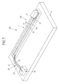
- Figure 7 illustrates a perspective view of an entire open-collector capable Mach-Zehnder-modulator device 200 comprising a modulator 100 according to the invention and a driver unit 30 configured to supply a (high frequency) differential voltage to the electrode arrangement 1 of modulator 100.
- the modulator 100 comprises the electrode arrangement 1 shown in Fig. 5 , i.e. comprising a monolithically integrated terminating network comprising the terminating resistors 21, 22, the metal structure 31 and the additional capacitor 40.
- the monolithic integration of the terminating resistors, the metal structure 31 and/or the additional capacitor 40 with the electrical lines 11, 12 is only optional.
- at least one of the group of the terminating resistor 21, 22, the metal structure 31 and/or the additional capacitor 40 is formed as a separate part, e.g. arranged on another substrate (e.g. a ceramic substrate) than the electrical lines 11, 12 and e.g. bonded to the electrical lines 11, 12 via bonding wires.
- the driver unit 30 (i.e. an output port of the driver unit 30) is electrically connected to the first and the second electrical line 11, 12 via a flexible coplanar line 50.
- the flexible coplanar line 50 comprises electrical lines 51, 52 arranged on a flexible, foil-like substrate 53 (e.g. formed from a polymer such as polyimide).
- the distance between the two (parallel) electrical lines 51, 52 is chosen to be small enough that the electrical lines 51, 52 from an electrical waveguide for conveying a high frequency electrical wave.
- the distance between the electrical lines 51, 52 is smaller than 100 ⁇ m or smaller than 50 ⁇ m.
- First endings of the electrical lines 51, 52 of the flexible coplanar line 50 are connected to an output port of the driver unit, whereas second endings of the electrical lines 51, 52 are connected to endings of the first and second electrical line 11, 12 of the modulator 100.
- the flexible coplanar strip 50 provides an electrical waveguide, its impedance can be better matched with the impedance of the driver unit 30 and the electrode arrangement 1 of the modulator such that the high frequency performance of the modulator can be improved. Due to its waveguide properties, in turn, the flexible coplanar strip 50 in contrast to bonding wires does not have to be very short such that a good thermal separation between the driver unit 30 (that may warm up during operation) and the modulator 100 can be realized.
- the driver unit 30 is arranged in a distance of at least 1 mm from the modulator 100.
Landscapes
- Physics & Mathematics (AREA)
- Nonlinear Science (AREA)
- General Physics & Mathematics (AREA)
- Optics & Photonics (AREA)
- Electromagnetism (AREA)
- Optical Modulation, Optical Deflection, Nonlinear Optics, Optical Demodulation, Optical Logic Elements (AREA)
Priority Applications (5)
| Application Number | Priority Date | Filing Date | Title |
|---|---|---|---|
| EP13194250.0A EP2876494B1 (fr) | 2013-11-25 | 2013-11-25 | Modulateur électro-optique |
| PCT/EP2014/075528 WO2015075260A1 (fr) | 2013-11-25 | 2014-11-25 | Modulateur électro-optique |
| US15/039,406 US9829765B2 (en) | 2013-11-25 | 2014-11-25 | Electro-optical modulator |
| CA2926708A CA2926708C (fr) | 2013-11-25 | 2014-11-25 | Modulateur electro-optique |
| JP2016554913A JP6411536B2 (ja) | 2013-11-25 | 2014-11-25 | 電気光学変調器 |
Applications Claiming Priority (1)
| Application Number | Priority Date | Filing Date | Title |
|---|---|---|---|
| EP13194250.0A EP2876494B1 (fr) | 2013-11-25 | 2013-11-25 | Modulateur électro-optique |
Publications (2)
| Publication Number | Publication Date |
|---|---|
| EP2876494A1 true EP2876494A1 (fr) | 2015-05-27 |
| EP2876494B1 EP2876494B1 (fr) | 2016-10-05 |
Family
ID=49667016
Family Applications (1)
| Application Number | Title | Priority Date | Filing Date |
|---|---|---|---|
| EP13194250.0A Active EP2876494B1 (fr) | 2013-11-25 | 2013-11-25 | Modulateur électro-optique |
Country Status (5)
| Country | Link |
|---|---|
| US (1) | US9829765B2 (fr) |
| EP (1) | EP2876494B1 (fr) |
| JP (1) | JP6411536B2 (fr) |
| CA (1) | CA2926708C (fr) |
| WO (1) | WO2015075260A1 (fr) |
Families Citing this family (1)
| Publication number | Priority date | Publication date | Assignee | Title |
|---|---|---|---|---|
| JP2020003600A (ja) * | 2018-06-27 | 2020-01-09 | 住友電気工業株式会社 | マッハツェンダ変調器 |
Citations (7)
| Publication number | Priority date | Publication date | Assignee | Title |
|---|---|---|---|---|
| JP2002333604A (ja) * | 2001-05-09 | 2002-11-22 | Sumitomo Osaka Cement Co Ltd | 導波路型光変調器 |
| US20030103709A1 (en) * | 2001-12-05 | 2003-06-05 | Jan Grinberg | Back biased electro-optical modulator |
| JP2010211060A (ja) * | 2009-03-11 | 2010-09-24 | Nippon Telegr & Teleph Corp <Ntt> | 光変調器 |
| WO2012175551A1 (fr) | 2011-06-20 | 2012-12-27 | Fraunhofer-Gesellschaft zur Förderung der angewandten Forschung e.V. | Modulateur électro-optique de type mach-zehnder et procédé de fabrication d'un modulateur électro-optique de type mach-zehnder |
| EP2615489A1 (fr) | 2012-01-12 | 2013-07-17 | Fraunhofer-Gesellschaft zur Förderung der angewandten Forschung e.V. | Agencement de modulateur de Mach-Zehnder et procédé de fonctionnement d'un agencement de modulateur de Mach-Zehnder |
| EP2615490A1 (fr) | 2012-01-12 | 2013-07-17 | Fraunhofer-Gesellschaft zur Förderung der angewandten Forschung e.V. | Agencement de modulateur de Mach-Zehnder et procédé de fonctionnement d'un agencement de modulateur de Mach-Zehnder |
| US20130209023A1 (en) * | 2012-02-15 | 2013-08-15 | Cogo Optronics, Inc. | Mach-zehnder optical modulator using a balanced coplanar stripline with lateral ground planes |
Family Cites Families (3)
| Publication number | Priority date | Publication date | Assignee | Title |
|---|---|---|---|---|
| US9146377B2 (en) * | 2010-01-13 | 2015-09-29 | The Aerospace Corporation | Photostructured optical devices and methods for making same |
| JP2012078759A (ja) * | 2010-10-06 | 2012-04-19 | Mitsubishi Electric Corp | 光変調器 |
| US8917958B2 (en) | 2011-12-22 | 2014-12-23 | Teraxion Inc. | Electrical waveguide transmission device for use with a mach-zehnder optical modulator |
-
2013
- 2013-11-25 EP EP13194250.0A patent/EP2876494B1/fr active Active
-
2014
- 2014-11-25 WO PCT/EP2014/075528 patent/WO2015075260A1/fr not_active Ceased
- 2014-11-25 CA CA2926708A patent/CA2926708C/fr active Active
- 2014-11-25 JP JP2016554913A patent/JP6411536B2/ja active Active
- 2014-11-25 US US15/039,406 patent/US9829765B2/en active Active
Patent Citations (7)
| Publication number | Priority date | Publication date | Assignee | Title |
|---|---|---|---|---|
| JP2002333604A (ja) * | 2001-05-09 | 2002-11-22 | Sumitomo Osaka Cement Co Ltd | 導波路型光変調器 |
| US20030103709A1 (en) * | 2001-12-05 | 2003-06-05 | Jan Grinberg | Back biased electro-optical modulator |
| JP2010211060A (ja) * | 2009-03-11 | 2010-09-24 | Nippon Telegr & Teleph Corp <Ntt> | 光変調器 |
| WO2012175551A1 (fr) | 2011-06-20 | 2012-12-27 | Fraunhofer-Gesellschaft zur Förderung der angewandten Forschung e.V. | Modulateur électro-optique de type mach-zehnder et procédé de fabrication d'un modulateur électro-optique de type mach-zehnder |
| EP2615489A1 (fr) | 2012-01-12 | 2013-07-17 | Fraunhofer-Gesellschaft zur Förderung der angewandten Forschung e.V. | Agencement de modulateur de Mach-Zehnder et procédé de fonctionnement d'un agencement de modulateur de Mach-Zehnder |
| EP2615490A1 (fr) | 2012-01-12 | 2013-07-17 | Fraunhofer-Gesellschaft zur Förderung der angewandten Forschung e.V. | Agencement de modulateur de Mach-Zehnder et procédé de fonctionnement d'un agencement de modulateur de Mach-Zehnder |
| US20130209023A1 (en) * | 2012-02-15 | 2013-08-15 | Cogo Optronics, Inc. | Mach-zehnder optical modulator using a balanced coplanar stripline with lateral ground planes |
Non-Patent Citations (2)
| Title |
|---|
| D. HOFFMANN: "45 GHz Bandwidth Travelling Wave Electrode Mach-Zehnder Modulator with Integrated Spot Size Converter", PROCEEDINGS INTERNATIONAL CONFERENCE ON INDIUM PHOSPHIDE AND RELATED MATERIALS, 2004, pages 585 |
| ROBERT G. WALKER: "High-Speed -V Semiconductor Intensity Modulators", IEEE JOURNAL OF QUANTUM ELECTRONICS, vol. 27, no. 3, March 1991 (1991-03-01) |
Also Published As
| Publication number | Publication date |
|---|---|
| CA2926708A1 (fr) | 2015-05-28 |
| JP2017502358A (ja) | 2017-01-19 |
| JP6411536B2 (ja) | 2018-10-24 |
| US20160349595A1 (en) | 2016-12-01 |
| EP2876494B1 (fr) | 2016-10-05 |
| CA2926708C (fr) | 2018-04-24 |
| WO2015075260A1 (fr) | 2015-05-28 |
| US9829765B2 (en) | 2017-11-28 |
Similar Documents
| Publication | Publication Date | Title |
|---|---|---|
| US9835927B2 (en) | Electro-optical modulator devices | |
| US9310663B2 (en) | Mach-zehnder modulator arrangement and method for operating a mach-zehnder modulator arrangement | |
| EP3079007B1 (fr) | Agencement de modulateur de mach-zehnder et procédé de fonctionnement d'un agencement de modulateur de mach-zehnder | |
| EP2629141B1 (fr) | Modulateur électro-optique et son procédé de fabrication | |
| EP3074813B1 (fr) | Agencement de ligne électrique | |
| JP3823873B2 (ja) | 半導体マッハツェンダ型光変調器 | |
| JP2016194544A (ja) | 広帯域導波路型光素子 | |
| EP2876494B1 (fr) | Modulateur électro-optique | |
| CN121411004A (zh) | 光调制器集成激光器元件、光调制电路以及光调制器 |
Legal Events
| Date | Code | Title | Description |
|---|---|---|---|
| PUAI | Public reference made under article 153(3) epc to a published international application that has entered the european phase |
Free format text: ORIGINAL CODE: 0009012 |
|
| 17P | Request for examination filed |
Effective date: 20131125 |
|
| AK | Designated contracting states |
Kind code of ref document: A1 Designated state(s): AL AT BE BG CH CY CZ DE DK EE ES FI FR GB GR HR HU IE IS IT LI LT LU LV MC MK MT NL NO PL PT RO RS SE SI SK SM TR |
|
| AX | Request for extension of the european patent |
Extension state: BA ME |
|
| R17P | Request for examination filed (corrected) |
Effective date: 20151124 |
|
| RBV | Designated contracting states (corrected) |
Designated state(s): AL AT BE BG CH CY CZ DE DK EE ES FI FR GB GR HR HU IE IS IT LI LT LU LV MC MK MT NL NO PL PT RO RS SE SI SK SM TR |
|
| GRAP | Despatch of communication of intention to grant a patent |
Free format text: ORIGINAL CODE: EPIDOSNIGR1 |
|
| INTG | Intention to grant announced |
Effective date: 20160502 |
|
| GRAS | Grant fee paid |
Free format text: ORIGINAL CODE: EPIDOSNIGR3 |
|
| GRAA | (expected) grant |
Free format text: ORIGINAL CODE: 0009210 |
|
| AK | Designated contracting states |
Kind code of ref document: B1 Designated state(s): AL AT BE BG CH CY CZ DE DK EE ES FI FR GB GR HR HU IE IS IT LI LT LU LV MC MK MT NL NO PL PT RO RS SE SI SK SM TR |
|
| REG | Reference to a national code |
Ref country code: GB Ref legal event code: FG4D |
|
| REG | Reference to a national code |
Ref country code: CH Ref legal event code: EP |
|
| REG | Reference to a national code |
Ref country code: AT Ref legal event code: REF Ref document number: 835122 Country of ref document: AT Kind code of ref document: T Effective date: 20161015 |
|
| REG | Reference to a national code |
Ref country code: IE Ref legal event code: FG4D |
|
| REG | Reference to a national code |
Ref country code: DE Ref legal event code: R096 Ref document number: 602013012367 Country of ref document: DE |
|
| REG | Reference to a national code |
Ref country code: FR Ref legal event code: PLFP Year of fee payment: 4 |
|
| REG | Reference to a national code |
Ref country code: NL Ref legal event code: MP Effective date: 20161005 |
|
| REG | Reference to a national code |
Ref country code: LT Ref legal event code: MG4D |
|
| PG25 | Lapsed in a contracting state [announced via postgrant information from national office to epo] |
Ref country code: LV Free format text: LAPSE BECAUSE OF FAILURE TO SUBMIT A TRANSLATION OF THE DESCRIPTION OR TO PAY THE FEE WITHIN THE PRESCRIBED TIME-LIMIT Effective date: 20161005 Ref country code: BE Free format text: LAPSE BECAUSE OF NON-PAYMENT OF DUE FEES Effective date: 20161130 |
|
| REG | Reference to a national code |
Ref country code: AT Ref legal event code: MK05 Ref document number: 835122 Country of ref document: AT Kind code of ref document: T Effective date: 20161005 |
|
| PG25 | Lapsed in a contracting state [announced via postgrant information from national office to epo] |
Ref country code: LT Free format text: LAPSE BECAUSE OF FAILURE TO SUBMIT A TRANSLATION OF THE DESCRIPTION OR TO PAY THE FEE WITHIN THE PRESCRIBED TIME-LIMIT Effective date: 20161005 Ref country code: NO Free format text: LAPSE BECAUSE OF FAILURE TO SUBMIT A TRANSLATION OF THE DESCRIPTION OR TO PAY THE FEE WITHIN THE PRESCRIBED TIME-LIMIT Effective date: 20170105 Ref country code: GR Free format text: LAPSE BECAUSE OF FAILURE TO SUBMIT A TRANSLATION OF THE DESCRIPTION OR TO PAY THE FEE WITHIN THE PRESCRIBED TIME-LIMIT Effective date: 20170106 Ref country code: SE Free format text: LAPSE BECAUSE OF FAILURE TO SUBMIT A TRANSLATION OF THE DESCRIPTION OR TO PAY THE FEE WITHIN THE PRESCRIBED TIME-LIMIT Effective date: 20161005 |
|
| PG25 | Lapsed in a contracting state [announced via postgrant information from national office to epo] |
Ref country code: HR Free format text: LAPSE BECAUSE OF FAILURE TO SUBMIT A TRANSLATION OF THE DESCRIPTION OR TO PAY THE FEE WITHIN THE PRESCRIBED TIME-LIMIT Effective date: 20161005 Ref country code: PL Free format text: LAPSE BECAUSE OF FAILURE TO SUBMIT A TRANSLATION OF THE DESCRIPTION OR TO PAY THE FEE WITHIN THE PRESCRIBED TIME-LIMIT Effective date: 20161005 Ref country code: PT Free format text: LAPSE BECAUSE OF FAILURE TO SUBMIT A TRANSLATION OF THE DESCRIPTION OR TO PAY THE FEE WITHIN THE PRESCRIBED TIME-LIMIT Effective date: 20170206 Ref country code: BE Free format text: LAPSE BECAUSE OF FAILURE TO SUBMIT A TRANSLATION OF THE DESCRIPTION OR TO PAY THE FEE WITHIN THE PRESCRIBED TIME-LIMIT Effective date: 20161005 Ref country code: NL Free format text: LAPSE BECAUSE OF FAILURE TO SUBMIT A TRANSLATION OF THE DESCRIPTION OR TO PAY THE FEE WITHIN THE PRESCRIBED TIME-LIMIT Effective date: 20161005 Ref country code: AT Free format text: LAPSE BECAUSE OF FAILURE TO SUBMIT A TRANSLATION OF THE DESCRIPTION OR TO PAY THE FEE WITHIN THE PRESCRIBED TIME-LIMIT Effective date: 20161005 Ref country code: RS Free format text: LAPSE BECAUSE OF FAILURE TO SUBMIT A TRANSLATION OF THE DESCRIPTION OR TO PAY THE FEE WITHIN THE PRESCRIBED TIME-LIMIT Effective date: 20161005 Ref country code: FI Free format text: LAPSE BECAUSE OF FAILURE TO SUBMIT A TRANSLATION OF THE DESCRIPTION OR TO PAY THE FEE WITHIN THE PRESCRIBED TIME-LIMIT Effective date: 20161005 Ref country code: IS Free format text: LAPSE BECAUSE OF FAILURE TO SUBMIT A TRANSLATION OF THE DESCRIPTION OR TO PAY THE FEE WITHIN THE PRESCRIBED TIME-LIMIT Effective date: 20170205 Ref country code: ES Free format text: LAPSE BECAUSE OF FAILURE TO SUBMIT A TRANSLATION OF THE DESCRIPTION OR TO PAY THE FEE WITHIN THE PRESCRIBED TIME-LIMIT Effective date: 20161005 |
|
| REG | Reference to a national code |
Ref country code: CH Ref legal event code: PL |
|
| REG | Reference to a national code |
Ref country code: DE Ref legal event code: R097 Ref document number: 602013012367 Country of ref document: DE |
|
| PG25 | Lapsed in a contracting state [announced via postgrant information from national office to epo] |
Ref country code: RO Free format text: LAPSE BECAUSE OF FAILURE TO SUBMIT A TRANSLATION OF THE DESCRIPTION OR TO PAY THE FEE WITHIN THE PRESCRIBED TIME-LIMIT Effective date: 20161005 Ref country code: MC Free format text: LAPSE BECAUSE OF FAILURE TO SUBMIT A TRANSLATION OF THE DESCRIPTION OR TO PAY THE FEE WITHIN THE PRESCRIBED TIME-LIMIT Effective date: 20161005 Ref country code: DK Free format text: LAPSE BECAUSE OF FAILURE TO SUBMIT A TRANSLATION OF THE DESCRIPTION OR TO PAY THE FEE WITHIN THE PRESCRIBED TIME-LIMIT Effective date: 20161005 Ref country code: CH Free format text: LAPSE BECAUSE OF NON-PAYMENT OF DUE FEES Effective date: 20161130 Ref country code: SK Free format text: LAPSE BECAUSE OF FAILURE TO SUBMIT A TRANSLATION OF THE DESCRIPTION OR TO PAY THE FEE WITHIN THE PRESCRIBED TIME-LIMIT Effective date: 20161005 Ref country code: EE Free format text: LAPSE BECAUSE OF FAILURE TO SUBMIT A TRANSLATION OF THE DESCRIPTION OR TO PAY THE FEE WITHIN THE PRESCRIBED TIME-LIMIT Effective date: 20161005 Ref country code: LI Free format text: LAPSE BECAUSE OF NON-PAYMENT OF DUE FEES Effective date: 20161130 Ref country code: CZ Free format text: LAPSE BECAUSE OF FAILURE TO SUBMIT A TRANSLATION OF THE DESCRIPTION OR TO PAY THE FEE WITHIN THE PRESCRIBED TIME-LIMIT Effective date: 20161005 |
|
| PLBE | No opposition filed within time limit |
Free format text: ORIGINAL CODE: 0009261 |
|
| STAA | Information on the status of an ep patent application or granted ep patent |
Free format text: STATUS: NO OPPOSITION FILED WITHIN TIME LIMIT |
|
| REG | Reference to a national code |
Ref country code: IE Ref legal event code: MM4A |
|
| PG25 | Lapsed in a contracting state [announced via postgrant information from national office to epo] |
Ref country code: IT Free format text: LAPSE BECAUSE OF FAILURE TO SUBMIT A TRANSLATION OF THE DESCRIPTION OR TO PAY THE FEE WITHIN THE PRESCRIBED TIME-LIMIT Effective date: 20161005 Ref country code: BG Free format text: LAPSE BECAUSE OF FAILURE TO SUBMIT A TRANSLATION OF THE DESCRIPTION OR TO PAY THE FEE WITHIN THE PRESCRIBED TIME-LIMIT Effective date: 20170105 Ref country code: SM Free format text: LAPSE BECAUSE OF FAILURE TO SUBMIT A TRANSLATION OF THE DESCRIPTION OR TO PAY THE FEE WITHIN THE PRESCRIBED TIME-LIMIT Effective date: 20161005 |
|
| 26N | No opposition filed |
Effective date: 20170706 |
|
| PG25 | Lapsed in a contracting state [announced via postgrant information from national office to epo] |
Ref country code: LU Free format text: LAPSE BECAUSE OF NON-PAYMENT OF DUE FEES Effective date: 20161130 |
|
| REG | Reference to a national code |
Ref country code: FR Ref legal event code: PLFP Year of fee payment: 5 |
|
| PG25 | Lapsed in a contracting state [announced via postgrant information from national office to epo] |
Ref country code: SI Free format text: LAPSE BECAUSE OF FAILURE TO SUBMIT A TRANSLATION OF THE DESCRIPTION OR TO PAY THE FEE WITHIN THE PRESCRIBED TIME-LIMIT Effective date: 20161005 Ref country code: IE Free format text: LAPSE BECAUSE OF NON-PAYMENT OF DUE FEES Effective date: 20161125 |
|
| PG25 | Lapsed in a contracting state [announced via postgrant information from national office to epo] |
Ref country code: HU Free format text: LAPSE BECAUSE OF FAILURE TO SUBMIT A TRANSLATION OF THE DESCRIPTION OR TO PAY THE FEE WITHIN THE PRESCRIBED TIME-LIMIT; INVALID AB INITIO Effective date: 20131125 |
|
| PG25 | Lapsed in a contracting state [announced via postgrant information from national office to epo] |
Ref country code: CY Free format text: LAPSE BECAUSE OF FAILURE TO SUBMIT A TRANSLATION OF THE DESCRIPTION OR TO PAY THE FEE WITHIN THE PRESCRIBED TIME-LIMIT Effective date: 20161005 Ref country code: MK Free format text: LAPSE BECAUSE OF FAILURE TO SUBMIT A TRANSLATION OF THE DESCRIPTION OR TO PAY THE FEE WITHIN THE PRESCRIBED TIME-LIMIT Effective date: 20161005 |
|
| PG25 | Lapsed in a contracting state [announced via postgrant information from national office to epo] |
Ref country code: MT Free format text: LAPSE BECAUSE OF NON-PAYMENT OF DUE FEES Effective date: 20161125 |
|
| PG25 | Lapsed in a contracting state [announced via postgrant information from national office to epo] |
Ref country code: TR Free format text: LAPSE BECAUSE OF FAILURE TO SUBMIT A TRANSLATION OF THE DESCRIPTION OR TO PAY THE FEE WITHIN THE PRESCRIBED TIME-LIMIT Effective date: 20161005 |
|
| PG25 | Lapsed in a contracting state [announced via postgrant information from national office to epo] |
Ref country code: AL Free format text: LAPSE BECAUSE OF FAILURE TO SUBMIT A TRANSLATION OF THE DESCRIPTION OR TO PAY THE FEE WITHIN THE PRESCRIBED TIME-LIMIT Effective date: 20161005 |
|
| P01 | Opt-out of the competence of the unified patent court (upc) registered |
Effective date: 20230524 |
|
| PGFP | Annual fee paid to national office [announced via postgrant information from national office to epo] |
Ref country code: DE Payment date: 20251118 Year of fee payment: 13 |
|
| PGFP | Annual fee paid to national office [announced via postgrant information from national office to epo] |
Ref country code: GB Payment date: 20251120 Year of fee payment: 13 |
|
| PGFP | Annual fee paid to national office [announced via postgrant information from national office to epo] |
Ref country code: FR Payment date: 20251120 Year of fee payment: 13 |