EP2876657A2 - Kontaktelemente für Mittel- bis Hochspannungsschalter - Google Patents
Kontaktelemente für Mittel- bis Hochspannungsschalter Download PDFInfo
- Publication number
- EP2876657A2 EP2876657A2 EP14189463.4A EP14189463A EP2876657A2 EP 2876657 A2 EP2876657 A2 EP 2876657A2 EP 14189463 A EP14189463 A EP 14189463A EP 2876657 A2 EP2876657 A2 EP 2876657A2
- Authority
- EP
- European Patent Office
- Prior art keywords
- switch
- conducting
- elements
- contact
- pin
- Prior art date
- Legal status (The legal status is an assumption and is not a legal conclusion. Google has not performed a legal analysis and makes no representation as to the accuracy of the status listed.)
- Granted
Links
Images


Classifications
-
- H—ELECTRICITY
- H01—ELECTRIC ELEMENTS
- H01H—ELECTRIC SWITCHES; RELAYS; SELECTORS; EMERGENCY PROTECTIVE DEVICES
- H01H1/00—Contacts
- H01H1/50—Means for increasing contact pressure, preventing vibration of contacts, holding contacts together after engagement, or biasing contacts to the open position
- H01H1/502—Means for increasing contact pressure, preventing vibration of contacts, holding contacts together after engagement, or biasing contacts to the open position the action of the contact pressure spring becoming active only after engagement of the contacts
-
- H—ELECTRICITY
- H01—ELECTRIC ELEMENTS
- H01H—ELECTRIC SWITCHES; RELAYS; SELECTORS; EMERGENCY PROTECTIVE DEVICES
- H01H33/00—High-tension or heavy-current switches with arc-extinguishing or arc-preventing means
- H01H33/60—Switches wherein the means for extinguishing or preventing the arc do not include separate means for obtaining or increasing flow of arc-extinguishing fluid
- H01H33/64—Switches wherein the means for extinguishing or preventing the arc do not include separate means for obtaining or increasing flow of arc-extinguishing fluid wherein the break is in gas
-
- H—ELECTRICITY
- H01—ELECTRIC ELEMENTS
- H01H—ELECTRIC SWITCHES; RELAYS; SELECTORS; EMERGENCY PROTECTIVE DEVICES
- H01H33/00—High-tension or heavy-current switches with arc-extinguishing or arc-preventing means
- H01H33/02—Details
- H01H2033/028—Details the cooperating contacts being both actuated simultaneously in opposite directions
Definitions
- the invention relates to a high or medium voltage switch, particularly a DC switch, comprising a first and a second set of contact elements that are mutually displaceable.
- the invention also relates to a current breaker comprising such a switch.
- a switch of this type is disclosed for example in the co-owned United States patents and published patent application US7235751 , US2012/0256711 , and US2013/0098874 . It has a first and a second set of contact elements and a drive adapted to mutually displace the contact elements along a displacement direction. Each contact element carries at least one conducting element. In a first mutual position of the contact elements, their conducting elements combine to form at least one conducting path between the first and second terminals of the switch, in a direction transversally to the displacement direction. In a second position of the contact elements, the conducting elements are mutually displaced into staggered positions and therefore the above conducting path is interrupted.
- the switches described in US2012/0256711 , and US2013/0098874 have contact elements with an insulating carrier carrying conducting elements.
- the conducting elements align to form one or more current paths between the terminals of the switch along an axial direction.
- the contact elements are mutually displaced by means of two drives along a direction perpendicular to the axial direction.
- the switching arrangement is arranged in a fluid-tight housing in a gas of elevated pressure or in a liquid.
- the switch has a high voltage withstand capability and fast switching times.
- the conducting element project over the two opposite surfaces of the carrier that carries it and are slightly movable in axial direction in respect to the carrier that carries it and/or it is slightly tiltable around a tilt axis, wherein said tilt axis is perpendicular to the axial direction and to the direction of displacement.
- Each terminal forms a contact surface for contacting the conducting elements, wherein at least one of the terminals comprises a spring member that elastically urges the contact surface of the terminal against the conducting elements. This ensures a proper contacting force between the conducting elements themselves and between the conducting elements and the contact surfaces and, with conducting elements being movable in axial direction the forces between all the conducting elements in a current path are substantially equal.
- the switch has at least a first terminal and a second terminal for applying the current to be switched and at least a first set of contact elements and a second set of contact elements and a drive adapted to mutually displace the sets of contact elements relatively to each other along a displacement direction with each contact element including an insulating carrier part that carries at least one conducting element with the positions of the conducting elements being such that in a first mutual position of the contact elements the conducting elements form at least one conducting path between the first terminal and the second terminal, i.e.
- the switch is in the closed, conducting position; and in a second mutual position of the contact elements the conducting elements are mutually displaced such that there is no conducting path formed by the conducting elements between the first terminal and the second terminal, i.e. the switch is in its opened, non-conducting position, with the conducting elements mounted onto the carrier part are locked into their operating position by one or more spring-loaded pins.
- the pin or pins are best rounded to allow for a small limited rotation movement of a main body of the conducting element around the central axis of the pin.
- the main body of the conducting element is slightly tiltable around a tilting axis, wherein said tilt axis is perpendicular to the axial direction and to the direction of displacement. This allows the conducting element to axially position itself accurately when the switch is in its first, closed position, thereby improving current conduction.
- the invention allows for a connection between the carrier and the conducting elements which is essentially free of hetero-material, in particular gluefree (free from glue).
- the main body is preferably an elongated rectangular cuboid with two long flattened contact faces oriented parallel to the plane of the contact element or its carrier part for contacting in operation the flattened contact face of a conducting element of an adjacent contact element.
- the cuboid main body has two further long faces and two small faces with such faces oriented in position perpendicular to the plane of the contact element.
- the small faces can have blind holes to mount the pins.
- an elastic element such as a spring is mounted behind the pins in the blind hole to facilitate the assembly and offer a latching action to lock the conducting element in its place on the contact element or carrier part.
- the conducting elements are mounted within openings of the carrier part with the pin or pins having a forked tip to latch onto a side wall of the opening.
- the openings are made preferably slightly wider than the distance between the second long faces or sides of the main body of the conducting elements, thus providing a small gap for a limited movement of the main body of the conducting elements within the opening of the carrier part in its mounted position.
- the pins are best made of a harder material than the main body, which in turn are typically manufactured using a material of high electrical conductivity such as silver, copper or aluminium.
- the pins themselves can be made of steel, preferably hardened steel or plastic material with a comparable hardness to steel.
- the term 'harder' is understood as a comparison of the hardness degree of different materials.
- the conducting element should advantageously project over the two opposite surfaces of the carrier that carries it.
- a conducting element projects above the surface of the surrounding carrier, it can be shown that the electrical field at the intersection between the surface and the conducting element is smaller than for a device where the surface of the conducting element is substantially flush with the surface of the carrier.
- Another aspect of the invention relates to the material used to manufacture the carrier part and/or a frame structure for the contact elements onto which frame the conducting elements can be mounted. It has been found that manufacturing the frame of the contact elements from an epoxy material reinforced by aramid fibers offers a superior performance in a DC switch as described above compared for example to the same structure manufactured from an epoxy material reinforced by glass fibers.
- the switch is advantageously used in high voltage applications (i.e. for voltages above 72 kV), but it can also be used for medium voltage applications (between some kV and 72 kV), particularly DC voltages.
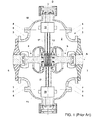
- the switch of Fig. 1 includes a fluid-tight housing 1 enclosing a space 2 filled with an insulating fluid, in particular SF 6 or air at elevated pressure or an oil.
- Housing 1 forms a GIS-type metallic enclosure of manifold type and comprises two tube sections.
- a first tube section 3 extends along an axial direction A, and a second tube section 4 extends along a direction D, which is called the displacement direction for reasons that will become apparent below.
- Axial direction A is perpendicular or nearly perpendicular to displacement direction D.
- the tube sections are formed by a substantially cross-shaped housing section 5.
- First tube section 3 ends in first and second support insulators 6 and 7, respectively.
- First support insulator 6 carries a first terminal 8 and second support insulator 7 carries a second terminal 9 of the switch.
- the two terminals 8, 9 extending through the support insulators 6, 7 carry the current through the switch, substantially along axial direction A.
- Second tube section 4 ends in a first and a second cap 10 and 11, respectively.
- First terminal 8 and second terminal 9 extend towards a center of space 2 and end at a distance from each other, with a switching arrangement 12 located between them, at the intersection region of first tube section 3 with second tube section 4.
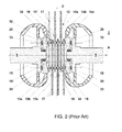
- switching arrangement 12 comprises a first set of contact elements 13a, 13b, 13c and a second set of contact elements 14a, 14b, 14c.
- each set comprises three contact elements, but that number may vary, and, for example, be two or more than three.
- the first and second set may also have different numbers of contact elements, e.g. two and three, respectively.
- the number is at least two contact elements per set.
- the contact elements of the two sets are stacked alternatingly, i.e. each contact element of one set is adjacent to two contact elements of the other set unless it is located at the end of switching arrangement 12, in which case it is located between one contact element of the other set and one of the terminals 8, 9.
- Each contact element comprises a plate-shaped insulating carrier 15, one or more conducting elements 16 and an actuator rod 17.
- each carrier 15 carries two conducting elements 16.
- Figs. 1 and 2 show the switch in the closed state with the contact elements 13a, 13b, 13c, 14a, 14b, 14c in a first mutual position, where the conducting elements 16 align to form two conducting paths 34 along axial direction A between the first and the second terminals 8, 9.
- the conducting paths 34 carry the current between the terminals 8, 9. Their number can be greater than one in order to increase continuous current carrying capability.
- the contact elements 13a, 13b, 13c, 14a, 14b, 14c are moved in operation along the displacement direction D into a second position, where the conducting elements 16 are staggered in respect to each other and do not form a conducting path.
- the position of the conducting elements in this second position is shown in dotted lines under reference number 16'.
- the conducting elements 16' are now separated from each other along direction D, thereby creating several contact gaps, thereby quickly providing a high dielectric withstand level.
- the actuator rods 17 are connected to two drives 18, 19.
- a first drive 18 is connected to the actuator rods 17 of the first set of contact elements 13a, 13b, 13c, and a second drive 19 is connected to the actuator rods 17 of the second set of contact elements 14a, 14b, 14c.
- the switch is opened by pulling the actuator rods 17 away from the center of the switch, thereby bringing the conducting elements into their second, staggered position.
- the rods 17 can be pushed towards the center of the switch, which also allows to bring the conducting elements into a staggered position.
- the drives 18, 19 can e.g. operate on the repulsive Lorentz-force principle and be of the type disclosed in US 7 235 751 , and they are therefore not described in detail herein.
- Each drive is able to displace one set of contact elements along the displacement direction D. They are adapted and controlled to move the first and second sets in opposite directions at the same time in order to increase the travelling length as well as acceleration and speed of displacement.
- the drives 18, 19 are arranged in opposite end regions of second tube section 4.
- the full stroke (e.g. 20 mm per drive) of the drives may not be necessary to travel in order for the contact system to provide the dielectric strength required, but a distance much shorter (e.g. 10 mm per drive), which can be reached in an even shorter time, suffices. This also provides certain safety in case of backtravel upon reaching the end-of-stroke position and damping phase of the actuators. A sufficient separation of the conducting elements 16 can be reached within 1 or 2 ms (milliseconds).
- each terminal 8, 9 carries a contact plate 32 forming a contact surface 33 contacting the conducting elements 16 when the switch is in its first position.
- the contact plates 32 are mounted to the terminals 8, 9 in axially displaceable manner, with springs 20 elastically urging the contact surface 33 against the conducting elements, thereby compressing the conducting elements 16 in their aligned state for better conduction.
- helical compression springs 20 are used for this purpose, but other types of spring members can be used as well.
- a compression force for the aligned conducting elements 16 can also be generated by means of a spring member (s) in only one of the terminals 8, 9 to reduce the contact resistance between the elements 16 in the closed position of the switch.
- FIG. 3A A perspective schematic view of a single contact element 13a prior to its full assembly is shown in FIG. 3A .
- the contact element includes a carrier part 15 and the actuator rod 17. In the example shown both parts are made together as a single part from the same material.
- the carrier part 15 has a frame structure with cut-out sections or holes 151, 152 to mount further conducting elements 16 and/or other elements.
- the carrier part 15 has a central opening 153 and further cut-out sections at one end to reduce the mass which has to be accelerated at each operation of the switch without reducing the mechanical stability unduly.
- the material used to make the frame structure of the contact element 13a of FIG. 3A is an epoxy resin reinforced with aramid fibers. Glass fiber reinforced epoxy materials have been found to be prone to electrically induced erosion processes and to lower insulation breakdown strength, which can be avoided with the epoxy resin reinforced with aramid fibers. The later material is still capable of withstanding the high acceleration forces during switching.
- This section includes a hole or opening 151 for the insertion of a conducting element 16 as described in the following.
- FIG. 4A is a cross-section of a main body 160 for use to manufacture a conducting element 16 for insertion into the carrier part 15 of a contact element such as the frame shown in FIG. 3A above.
- the main body 160 of conducting element 16 has essentially a rectangular cuboid shape with an aspect ratio of approximately 5:1. It is made of aluminium coated with a silver layer. Both ends or small faces of the main body 160 are machined into semi-spherical shape. All edges of the main body 160 are rounded.
- the shape of the main body 160 is chosen such that the width in direction of the displacement is small to ensure that conducting elements 16 can be separated with a correspondingly small displacement of the contact elements 13a -14c.
- a cross-section of the main body 160 of a conducting element 16 is shown with a blind bore or hole 163 drilled into each of the rounded ends or small faces.
- the bore 163 is used to accommodate a spring 161 and a pin 162.
- FIG. 4C A cross-section of such a pin 162 is shown in FIG. 4C . It has an essentially cylindrical shape with one rounded end. A central cut 164 is machined into the rounded end rendering this end of the pin into a two pronged fork. The in radial direction outer corners of each prong are again all rounded.
- FIG. 3A A fully mounted conducting element 16 within the frame structure of a contact element 13a (as shown in FIG. 3A ) is illustrated in figures 3B and 3C , with FIG. 3B showing a perspective view on an enlarged section of FIG. 3A with a conducting element 16 inserted into the pre-cut hole 151 of the carrier 15 of the contact element 13a. Due the manufacturing steps as described above, all external exposed edges and corners are rounded, thus providing a better protection against discharges and/or arc-forming in a medium and high voltage environment.
- FIG. 3C The cross-section along the dash-dotted line X-X in FIG. 3B and perpendicular to the plane of the opening 151 within the frame structure of the contact element 13a (as shown in FIG. 3A ) and with an conducting element 16 inserted is shown in FIG. 3C .
- the conducting element 16 is shown in its assembled and mounted state.
- the conducting element 16 includes the main body 160 and two pins each inserted into one of the blind holes 163 at either end of the main body. Also located within the blind hole 163 is a springy or an elastic element 161. In the absence of forces the springy element 161 pushes the upper, forked part of the pin 162 in direction out of its blind hole.
- a conducting element 16 as described can be mounted into an opening 151 and thus onto the carrier 15 of a contact element by exerting a force on the pin or pins 162 and by releasing this force, after the conducting element is in its desired position. After the release of the force, the pins loch against the walls of the opening 151. The width of the cut 164 in each pin is matched by the thickness of carrier wall at this location. Thus a secure fastening is achieved without any further fastening means such as screws or glues. At the same time, each contact element can be easily assembled and conducting elements can be easily mounted or replaced.
- the pin can be designed, for example with a smaller pin at the top, to be inserted into holes within the side wall of the openings 151.
- this alternative is considered inferior to the example presented above as it further weakens the structural integrity of the carrier part 15 or requires at least a local increase in its thickness.
- each pin 162 enable small tilting movements of the main body 161 out of the plane of the carrier part 15. This aspect becomes important when the conducting elements 16 of two adjacent contact elements, e.g. contact element 13a and 14a of FIG. 1 come into contact during the closing or opening of the switch.
- the tilting ensures that in the final closed position the flattened long sides of the main body 160 are fully in contact with each other and thus reduce the contact resistance and limit the heat generated at the interface between the neighbouring conducting elements (16).
- a switch with spacer elements as described above has applications for example in a high voltage circuit breaker as illustrated in the FIG. 5 and described in the accompanying text of US 2013/0098874 .
- the switch is connected in series with solid state breakers and in parallel with a second set of solid state breakers.
Landscapes
- Push-Button Switches (AREA)
- Contacts (AREA)
- Switch Cases, Indication, And Locking (AREA)
- Arc-Extinguishing Devices That Are Switches (AREA)
Priority Applications (1)
| Application Number | Priority Date | Filing Date | Title |
|---|---|---|---|
| EP14189463.4A EP2876657B1 (de) | 2013-11-26 | 2014-10-20 | Kontaktelemente für Mittel- bis Hochspannungsschalter |
Applications Claiming Priority (2)
| Application Number | Priority Date | Filing Date | Title |
|---|---|---|---|
| EP13194428 | 2013-11-26 | ||
| EP14189463.4A EP2876657B1 (de) | 2013-11-26 | 2014-10-20 | Kontaktelemente für Mittel- bis Hochspannungsschalter |
Publications (3)
| Publication Number | Publication Date |
|---|---|
| EP2876657A2 true EP2876657A2 (de) | 2015-05-27 |
| EP2876657A3 EP2876657A3 (de) | 2015-08-26 |
| EP2876657B1 EP2876657B1 (de) | 2021-07-07 |
Family
ID=49626871
Family Applications (1)
| Application Number | Title | Priority Date | Filing Date |
|---|---|---|---|
| EP14189463.4A Active EP2876657B1 (de) | 2013-11-26 | 2014-10-20 | Kontaktelemente für Mittel- bis Hochspannungsschalter |
Country Status (2)
| Country | Link |
|---|---|
| EP (1) | EP2876657B1 (de) |
| CN (1) | CN104681330B (de) |
Families Citing this family (1)
| Publication number | Priority date | Publication date | Assignee | Title |
|---|---|---|---|---|
| CN110473735B (zh) * | 2017-07-24 | 2021-04-02 | 许继集团有限公司 | 隔离开关及其动触头 |
Citations (3)
| Publication number | Priority date | Publication date | Assignee | Title |
|---|---|---|---|---|
| US7235751B2 (en) | 2001-01-11 | 2007-06-26 | Abb Ab | Electric device, a current limiter and an electric power network |
| US20120256711A1 (en) | 2011-04-11 | 2012-10-11 | Abb Technology Ag | Switch having two sets of contact elements and two drives |
| US20130098874A1 (en) | 2011-04-11 | 2013-04-25 | Abb Technology Ag | Switch having two sets of contact elements |
Family Cites Families (4)
| Publication number | Priority date | Publication date | Assignee | Title |
|---|---|---|---|---|
| US2894095A (en) * | 1954-07-08 | 1959-07-07 | Ericsson Telefon Ab L M | Contact device |
| DE1229170B (de) * | 1964-11-11 | 1966-11-24 | Reinhausen Kg Maschf | Kontaktanordnung fuer stromlos unterbrechende Schalter |
| DE2210626A1 (de) * | 1972-03-06 | 1973-09-20 | Licentia Gmbh | Isolierstuetzer fuer druckgasisolierte, metallgekapselte hochspannungs-schaltanlagen |
| WO2010037424A1 (en) * | 2008-10-03 | 2010-04-08 | Abb Technology Ag | Electric current limiting device |
-
2014
- 2014-10-20 EP EP14189463.4A patent/EP2876657B1/de active Active
- 2014-11-26 CN CN201410703318.6A patent/CN104681330B/zh active Active
Patent Citations (3)
| Publication number | Priority date | Publication date | Assignee | Title |
|---|---|---|---|---|
| US7235751B2 (en) | 2001-01-11 | 2007-06-26 | Abb Ab | Electric device, a current limiter and an electric power network |
| US20120256711A1 (en) | 2011-04-11 | 2012-10-11 | Abb Technology Ag | Switch having two sets of contact elements and two drives |
| US20130098874A1 (en) | 2011-04-11 | 2013-04-25 | Abb Technology Ag | Switch having two sets of contact elements |
Also Published As
| Publication number | Publication date |
|---|---|
| CN104681330B (zh) | 2018-04-24 |
| EP2876657B1 (de) | 2021-07-07 |
| EP2876657A3 (de) | 2015-08-26 |
| CN104681330A (zh) | 2015-06-03 |
Similar Documents
| Publication | Publication Date | Title |
|---|---|---|
| KR101867101B1 (ko) | 2 개의 접촉 요소 세트 및 2 개의 드라이브를 갖는 스위치 | |
| KR101867100B1 (ko) | 2 개의 접촉 요소 세트를 갖는 스위치 | |
| EP2546848B1 (de) | Schnellschalter mit nicht kreisförmiger Thomson-Spule | |
| EP2876657B1 (de) | Kontaktelemente für Mittel- bis Hochspannungsschalter | |
| EP2876659B1 (de) | Schalter mit zwei Sätzen an Kontaktelementen | |
| CN104885179B (zh) | 开关组件 | |
| SE1400421A1 (sv) | Contact Elements for Medium to High Voltage Switches | |
| EP3776616B1 (de) | Federbelastetes hilfskontaktsystem für busübertragungsschaltung in einem drehtrennschalter | |
| KR20230014751A (ko) | 진동 감소 유도 제어가 있는 진공 벌브 스위치 | |
| EP3073501B1 (de) | Linearer mehrpoliger schalter | |
| US20130119022A1 (en) | Medium and high-voltage electric switch with return on closure and an insertion device for inserting a resistance | |
| KR20200022073A (ko) | 전자기력 디바이스 | |
| KR20200022072A (ko) | 전자기력 디바이스 | |
| WO2015070334A1 (en) | Electrical contacts with a reduced aluminum section |
Legal Events
| Date | Code | Title | Description |
|---|---|---|---|
| PUAI | Public reference made under article 153(3) epc to a published international application that has entered the european phase |
Free format text: ORIGINAL CODE: 0009012 |
|
| 17P | Request for examination filed |
Effective date: 20141020 |
|
| AK | Designated contracting states |
Kind code of ref document: A2 Designated state(s): AL AT BE BG CH CY CZ DE DK EE ES FI FR GB GR HR HU IE IS IT LI LT LU LV MC MK MT NL NO PL PT RO RS SE SI SK SM TR |
|
| AX | Request for extension of the european patent |
Extension state: BA ME |
|
| PUAL | Search report despatched |
Free format text: ORIGINAL CODE: 0009013 |
|
| AK | Designated contracting states |
Kind code of ref document: A3 Designated state(s): AL AT BE BG CH CY CZ DE DK EE ES FI FR GB GR HR HU IE IS IT LI LT LU LV MC MK MT NL NO PL PT RO RS SE SI SK SM TR |
|
| AX | Request for extension of the european patent |
Extension state: BA ME |
|
| RIC1 | Information provided on ipc code assigned before grant |
Ipc: H01H 33/64 20060101ALI20150722BHEP Ipc: H01H 1/50 20060101AFI20150722BHEP |
|
| R17P | Request for examination filed (corrected) |
Effective date: 20160225 |
|
| RBV | Designated contracting states (corrected) |
Designated state(s): AL AT BE BG CH CY CZ DE DK EE ES FI FR GB GR HR HU IE IS IT LI LT LU LV MC MK MT NL NO PL PT RO RS SE SI SK SM TR |
|
| RAP1 | Party data changed (applicant data changed or rights of an application transferred) |
Owner name: ABB SCHWEIZ AG |
|
| STAA | Information on the status of an ep patent application or granted ep patent |
Free format text: STATUS: EXAMINATION IS IN PROGRESS |
|
| 17Q | First examination report despatched |
Effective date: 20180109 |
|
| RAP1 | Party data changed (applicant data changed or rights of an application transferred) |
Owner name: ABB POWER GRIDS SWITZERLAND AG |
|
| GRAP | Despatch of communication of intention to grant a patent |
Free format text: ORIGINAL CODE: EPIDOSNIGR1 |
|
| STAA | Information on the status of an ep patent application or granted ep patent |
Free format text: STATUS: GRANT OF PATENT IS INTENDED |
|
| INTG | Intention to grant announced |
Effective date: 20210128 |
|
| GRAS | Grant fee paid |
Free format text: ORIGINAL CODE: EPIDOSNIGR3 |
|
| GRAA | (expected) grant |
Free format text: ORIGINAL CODE: 0009210 |
|
| STAA | Information on the status of an ep patent application or granted ep patent |
Free format text: STATUS: THE PATENT HAS BEEN GRANTED |
|
| AK | Designated contracting states |
Kind code of ref document: B1 Designated state(s): AL AT BE BG CH CY CZ DE DK EE ES FI FR GB GR HR HU IE IS IT LI LT LU LV MC MK MT NL NO PL PT RO RS SE SI SK SM TR |
|
| REG | Reference to a national code |
Ref country code: GB Ref legal event code: FG4D |
|
| REG | Reference to a national code |
Ref country code: AT Ref legal event code: REF Ref document number: 1409385 Country of ref document: AT Kind code of ref document: T Effective date: 20210715 |
|
| REG | Reference to a national code |
Ref country code: DE Ref legal event code: R096 Ref document number: 602014078571 Country of ref document: DE |
|
| REG | Reference to a national code |
Ref country code: IE Ref legal event code: FG4D |
|
| REG | Reference to a national code |
Ref country code: LT Ref legal event code: MG9D |
|
| REG | Reference to a national code |
Ref country code: NL Ref legal event code: MP Effective date: 20210707 |
|
| REG | Reference to a national code |
Ref country code: AT Ref legal event code: MK05 Ref document number: 1409385 Country of ref document: AT Kind code of ref document: T Effective date: 20210707 |
|
| RAP4 | Party data changed (patent owner data changed or rights of a patent transferred) |
Owner name: HITACHI ENERGY SWITZERLAND AG |
|
| PG25 | Lapsed in a contracting state [announced via postgrant information from national office to epo] |
Ref country code: LT Free format text: LAPSE BECAUSE OF FAILURE TO SUBMIT A TRANSLATION OF THE DESCRIPTION OR TO PAY THE FEE WITHIN THE PRESCRIBED TIME-LIMIT Effective date: 20210707 Ref country code: BG Free format text: LAPSE BECAUSE OF FAILURE TO SUBMIT A TRANSLATION OF THE DESCRIPTION OR TO PAY THE FEE WITHIN THE PRESCRIBED TIME-LIMIT Effective date: 20211007 Ref country code: AT Free format text: LAPSE BECAUSE OF FAILURE TO SUBMIT A TRANSLATION OF THE DESCRIPTION OR TO PAY THE FEE WITHIN THE PRESCRIBED TIME-LIMIT Effective date: 20210707 Ref country code: NO Free format text: LAPSE BECAUSE OF FAILURE TO SUBMIT A TRANSLATION OF THE DESCRIPTION OR TO PAY THE FEE WITHIN THE PRESCRIBED TIME-LIMIT Effective date: 20211007 Ref country code: PT Free format text: LAPSE BECAUSE OF FAILURE TO SUBMIT A TRANSLATION OF THE DESCRIPTION OR TO PAY THE FEE WITHIN THE PRESCRIBED TIME-LIMIT Effective date: 20211108 Ref country code: NL Free format text: LAPSE BECAUSE OF FAILURE TO SUBMIT A TRANSLATION OF THE DESCRIPTION OR TO PAY THE FEE WITHIN THE PRESCRIBED TIME-LIMIT Effective date: 20210707 Ref country code: ES Free format text: LAPSE BECAUSE OF FAILURE TO SUBMIT A TRANSLATION OF THE DESCRIPTION OR TO PAY THE FEE WITHIN THE PRESCRIBED TIME-LIMIT Effective date: 20210707 Ref country code: FI Free format text: LAPSE BECAUSE OF FAILURE TO SUBMIT A TRANSLATION OF THE DESCRIPTION OR TO PAY THE FEE WITHIN THE PRESCRIBED TIME-LIMIT Effective date: 20210707 Ref country code: HR Free format text: LAPSE BECAUSE OF FAILURE TO SUBMIT A TRANSLATION OF THE DESCRIPTION OR TO PAY THE FEE WITHIN THE PRESCRIBED TIME-LIMIT Effective date: 20210707 Ref country code: RS Free format text: LAPSE BECAUSE OF FAILURE TO SUBMIT A TRANSLATION OF THE DESCRIPTION OR TO PAY THE FEE WITHIN THE PRESCRIBED TIME-LIMIT Effective date: 20210707 Ref country code: SE Free format text: LAPSE BECAUSE OF FAILURE TO SUBMIT A TRANSLATION OF THE DESCRIPTION OR TO PAY THE FEE WITHIN THE PRESCRIBED TIME-LIMIT Effective date: 20210707 |
|
| PG25 | Lapsed in a contracting state [announced via postgrant information from national office to epo] |
Ref country code: PL Free format text: LAPSE BECAUSE OF FAILURE TO SUBMIT A TRANSLATION OF THE DESCRIPTION OR TO PAY THE FEE WITHIN THE PRESCRIBED TIME-LIMIT Effective date: 20210707 Ref country code: LV Free format text: LAPSE BECAUSE OF FAILURE TO SUBMIT A TRANSLATION OF THE DESCRIPTION OR TO PAY THE FEE WITHIN THE PRESCRIBED TIME-LIMIT Effective date: 20210707 Ref country code: GR Free format text: LAPSE BECAUSE OF FAILURE TO SUBMIT A TRANSLATION OF THE DESCRIPTION OR TO PAY THE FEE WITHIN THE PRESCRIBED TIME-LIMIT Effective date: 20211008 |
|
| REG | Reference to a national code |
Ref country code: DE Ref legal event code: R097 Ref document number: 602014078571 Country of ref document: DE |
|
| PG25 | Lapsed in a contracting state [announced via postgrant information from national office to epo] |
Ref country code: DK Free format text: LAPSE BECAUSE OF FAILURE TO SUBMIT A TRANSLATION OF THE DESCRIPTION OR TO PAY THE FEE WITHIN THE PRESCRIBED TIME-LIMIT Effective date: 20210707 |
|
| PLBE | No opposition filed within time limit |
Free format text: ORIGINAL CODE: 0009261 |
|
| STAA | Information on the status of an ep patent application or granted ep patent |
Free format text: STATUS: NO OPPOSITION FILED WITHIN TIME LIMIT |
|
| REG | Reference to a national code |
Ref country code: CH Ref legal event code: PL |
|
| PG25 | Lapsed in a contracting state [announced via postgrant information from national office to epo] |
Ref country code: SM Free format text: LAPSE BECAUSE OF FAILURE TO SUBMIT A TRANSLATION OF THE DESCRIPTION OR TO PAY THE FEE WITHIN THE PRESCRIBED TIME-LIMIT Effective date: 20210707 Ref country code: SK Free format text: LAPSE BECAUSE OF FAILURE TO SUBMIT A TRANSLATION OF THE DESCRIPTION OR TO PAY THE FEE WITHIN THE PRESCRIBED TIME-LIMIT Effective date: 20210707 Ref country code: RO Free format text: LAPSE BECAUSE OF FAILURE TO SUBMIT A TRANSLATION OF THE DESCRIPTION OR TO PAY THE FEE WITHIN THE PRESCRIBED TIME-LIMIT Effective date: 20210707 Ref country code: EE Free format text: LAPSE BECAUSE OF FAILURE TO SUBMIT A TRANSLATION OF THE DESCRIPTION OR TO PAY THE FEE WITHIN THE PRESCRIBED TIME-LIMIT Effective date: 20210707 Ref country code: CZ Free format text: LAPSE BECAUSE OF FAILURE TO SUBMIT A TRANSLATION OF THE DESCRIPTION OR TO PAY THE FEE WITHIN THE PRESCRIBED TIME-LIMIT Effective date: 20210707 Ref country code: AL Free format text: LAPSE BECAUSE OF FAILURE TO SUBMIT A TRANSLATION OF THE DESCRIPTION OR TO PAY THE FEE WITHIN THE PRESCRIBED TIME-LIMIT Effective date: 20210707 |
|
| 26N | No opposition filed |
Effective date: 20220408 |
|
| REG | Reference to a national code |
Ref country code: DE Ref legal event code: R081 Ref document number: 602014078571 Country of ref document: DE Owner name: HITACHI ENERGY SWITZERLAND AG, CH Free format text: FORMER OWNER: ABB POWER GRIDS SWITZERLAND AG, BADEN, CH Ref country code: DE Ref legal event code: R081 Ref document number: 602014078571 Country of ref document: DE Owner name: HITACHI ENERGY LTD, CH Free format text: FORMER OWNER: ABB POWER GRIDS SWITZERLAND AG, BADEN, CH |
|
| REG | Reference to a national code |
Ref country code: BE Ref legal event code: MM Effective date: 20211031 |
|
| PG25 | Lapsed in a contracting state [announced via postgrant information from national office to epo] |
Ref country code: MC Free format text: LAPSE BECAUSE OF FAILURE TO SUBMIT A TRANSLATION OF THE DESCRIPTION OR TO PAY THE FEE WITHIN THE PRESCRIBED TIME-LIMIT Effective date: 20210707 |
|
| PG25 | Lapsed in a contracting state [announced via postgrant information from national office to epo] |
Ref country code: LU Free format text: LAPSE BECAUSE OF NON-PAYMENT OF DUE FEES Effective date: 20211020 Ref country code: IT Free format text: LAPSE BECAUSE OF FAILURE TO SUBMIT A TRANSLATION OF THE DESCRIPTION OR TO PAY THE FEE WITHIN THE PRESCRIBED TIME-LIMIT Effective date: 20210707 Ref country code: BE Free format text: LAPSE BECAUSE OF NON-PAYMENT OF DUE FEES Effective date: 20211031 |
|
| PG25 | Lapsed in a contracting state [announced via postgrant information from national office to epo] |
Ref country code: LI Free format text: LAPSE BECAUSE OF NON-PAYMENT OF DUE FEES Effective date: 20211031 Ref country code: CH Free format text: LAPSE BECAUSE OF NON-PAYMENT OF DUE FEES Effective date: 20211031 |
|
| PG25 | Lapsed in a contracting state [announced via postgrant information from national office to epo] |
Ref country code: IE Free format text: LAPSE BECAUSE OF NON-PAYMENT OF DUE FEES Effective date: 20211020 |
|
| PG25 | Lapsed in a contracting state [announced via postgrant information from national office to epo] |
Ref country code: HU Free format text: LAPSE BECAUSE OF FAILURE TO SUBMIT A TRANSLATION OF THE DESCRIPTION OR TO PAY THE FEE WITHIN THE PRESCRIBED TIME-LIMIT; INVALID AB INITIO Effective date: 20141020 |
|
| PG25 | Lapsed in a contracting state [announced via postgrant information from national office to epo] |
Ref country code: CY Free format text: LAPSE BECAUSE OF FAILURE TO SUBMIT A TRANSLATION OF THE DESCRIPTION OR TO PAY THE FEE WITHIN THE PRESCRIBED TIME-LIMIT Effective date: 20210707 |
|
| P01 | Opt-out of the competence of the unified patent court (upc) registered |
Effective date: 20230527 |
|
| REG | Reference to a national code |
Ref country code: DE Ref legal event code: R082 Ref document number: 602014078571 Country of ref document: DE Representative=s name: DENNEMEYER & ASSOCIATES RECHTSANWALTSGESELLSCH, DE Ref country code: DE Ref legal event code: R082 Ref document number: 602014078571 Country of ref document: DE Representative=s name: DENNEMEYER & ASSOCIATES S.A., DE Ref country code: DE Ref legal event code: R081 Ref document number: 602014078571 Country of ref document: DE Owner name: HITACHI ENERGY LTD, CH Free format text: FORMER OWNER: HITACHI ENERGY SWITZERLAND AG, BADEN, CH |
|
| PG25 | Lapsed in a contracting state [announced via postgrant information from national office to epo] |
Ref country code: MK Free format text: LAPSE BECAUSE OF FAILURE TO SUBMIT A TRANSLATION OF THE DESCRIPTION OR TO PAY THE FEE WITHIN THE PRESCRIBED TIME-LIMIT Effective date: 20210707 |
|
| PG25 | Lapsed in a contracting state [announced via postgrant information from national office to epo] |
Ref country code: TR Free format text: LAPSE BECAUSE OF FAILURE TO SUBMIT A TRANSLATION OF THE DESCRIPTION OR TO PAY THE FEE WITHIN THE PRESCRIBED TIME-LIMIT Effective date: 20210707 |
|
| REG | Reference to a national code |
Ref country code: GB Ref legal event code: 732E Free format text: REGISTERED BETWEEN 20240718 AND 20240724 |
|
| PG25 | Lapsed in a contracting state [announced via postgrant information from national office to epo] |
Ref country code: MT Free format text: LAPSE BECAUSE OF FAILURE TO SUBMIT A TRANSLATION OF THE DESCRIPTION OR TO PAY THE FEE WITHIN THE PRESCRIBED TIME-LIMIT Effective date: 20210707 |
|
| REG | Reference to a national code |
Ref country code: DE Ref legal event code: R082 Ref document number: 602014078571 Country of ref document: DE Representative=s name: DENNEMEYER & ASSOCIATES RECHTSANWALTSGESELLSCH, DE |
|
| PGFP | Annual fee paid to national office [announced via postgrant information from national office to epo] |
Ref country code: DE Payment date: 20251021 Year of fee payment: 12 |
|
| PGFP | Annual fee paid to national office [announced via postgrant information from national office to epo] |
Ref country code: GB Payment date: 20251022 Year of fee payment: 12 |
|
| PGFP | Annual fee paid to national office [announced via postgrant information from national office to epo] |
Ref country code: FR Payment date: 20251030 Year of fee payment: 12 |