EP2876684A2 - Dispositif électroluminescent organique et son procédé de réparation - Google Patents
Dispositif électroluminescent organique et son procédé de réparation Download PDFInfo
- Publication number
- EP2876684A2 EP2876684A2 EP14181215.6A EP14181215A EP2876684A2 EP 2876684 A2 EP2876684 A2 EP 2876684A2 EP 14181215 A EP14181215 A EP 14181215A EP 2876684 A2 EP2876684 A2 EP 2876684A2
- Authority
- EP
- European Patent Office
- Prior art keywords
- electrode
- driving tft
- tft
- pixel
- region
- Prior art date
- Legal status (The legal status is an assumption and is not a legal conclusion. Google has not performed a legal analysis and makes no representation as to the accuracy of the status listed.)
- Granted
Links
Images



Classifications
-
- H—ELECTRICITY
- H10—SEMICONDUCTOR DEVICES; ELECTRIC SOLID-STATE DEVICES NOT OTHERWISE PROVIDED FOR
- H10K—ORGANIC ELECTRIC SOLID-STATE DEVICES
- H10K59/00—Integrated devices, or assemblies of multiple devices, comprising at least one organic light-emitting element covered by group H10K50/00
- H10K59/80—Constructional details
-
- H—ELECTRICITY
- H10—SEMICONDUCTOR DEVICES; ELECTRIC SOLID-STATE DEVICES NOT OTHERWISE PROVIDED FOR
- H10K—ORGANIC ELECTRIC SOLID-STATE DEVICES
- H10K59/00—Integrated devices, or assemblies of multiple devices, comprising at least one organic light-emitting element covered by group H10K50/00
- H10K59/10—OLED displays
- H10K59/12—Active-matrix OLED [AMOLED] displays
- H10K59/121—Active-matrix OLED [AMOLED] displays characterised by the geometry or disposition of pixel elements
-
- B—PERFORMING OPERATIONS; TRANSPORTING
- B23—MACHINE TOOLS; METAL-WORKING NOT OTHERWISE PROVIDED FOR
- B23K—SOLDERING OR UNSOLDERING; WELDING; CLADDING OR PLATING BY SOLDERING OR WELDING; CUTTING BY APPLYING HEAT LOCALLY, e.g. FLAME CUTTING; WORKING BY LASER BEAM
- B23K26/00—Working by laser beam, e.g. welding, cutting or boring
- B23K26/36—Removing material
- B23K26/38—Removing material by boring or cutting
-
- H—ELECTRICITY
- H10—SEMICONDUCTOR DEVICES; ELECTRIC SOLID-STATE DEVICES NOT OTHERWISE PROVIDED FOR
- H10D—INORGANIC ELECTRIC SEMICONDUCTOR DEVICES
- H10D30/00—Field-effect transistors [FET]
- H10D30/60—Insulated-gate field-effect transistors [IGFET]
- H10D30/67—Thin-film transistors [TFT]
- H10D30/6729—Thin-film transistors [TFT] characterised by the electrodes
-
- H—ELECTRICITY
- H10—SEMICONDUCTOR DEVICES; ELECTRIC SOLID-STATE DEVICES NOT OTHERWISE PROVIDED FOR
- H10K—ORGANIC ELECTRIC SOLID-STATE DEVICES
- H10K50/00—Organic light-emitting devices
- H10K50/80—Constructional details
- H10K50/805—Electrodes
- H10K50/81—Anodes
- H10K50/813—Anodes characterised by their shape
-
- H—ELECTRICITY
- H10—SEMICONDUCTOR DEVICES; ELECTRIC SOLID-STATE DEVICES NOT OTHERWISE PROVIDED FOR
- H10K—ORGANIC ELECTRIC SOLID-STATE DEVICES
- H10K50/00—Organic light-emitting devices
- H10K50/80—Constructional details
- H10K50/84—Passivation; Containers; Encapsulations
-
- H—ELECTRICITY
- H10—SEMICONDUCTOR DEVICES; ELECTRIC SOLID-STATE DEVICES NOT OTHERWISE PROVIDED FOR
- H10K—ORGANIC ELECTRIC SOLID-STATE DEVICES
- H10K59/00—Integrated devices, or assemblies of multiple devices, comprising at least one organic light-emitting element covered by group H10K50/00
- H10K59/10—OLED displays
- H10K59/12—Active-matrix OLED [AMOLED] displays
- H10K59/1201—Manufacture or treatment
-
- H—ELECTRICITY
- H10—SEMICONDUCTOR DEVICES; ELECTRIC SOLID-STATE DEVICES NOT OTHERWISE PROVIDED FOR
- H10K—ORGANIC ELECTRIC SOLID-STATE DEVICES
- H10K59/00—Integrated devices, or assemblies of multiple devices, comprising at least one organic light-emitting element covered by group H10K50/00
- H10K59/10—OLED displays
- H10K59/12—Active-matrix OLED [AMOLED] displays
- H10K59/121—Active-matrix OLED [AMOLED] displays characterised by the geometry or disposition of pixel elements
- H10K59/1213—Active-matrix OLED [AMOLED] displays characterised by the geometry or disposition of pixel elements the pixel elements being TFTs
-
- H—ELECTRICITY
- H10—SEMICONDUCTOR DEVICES; ELECTRIC SOLID-STATE DEVICES NOT OTHERWISE PROVIDED FOR
- H10K—ORGANIC ELECTRIC SOLID-STATE DEVICES
- H10K59/00—Integrated devices, or assemblies of multiple devices, comprising at least one organic light-emitting element covered by group H10K50/00
- H10K59/10—OLED displays
- H10K59/12—Active-matrix OLED [AMOLED] displays
- H10K59/123—Connection of the pixel electrodes to the thin film transistors [TFT]
-
- H—ELECTRICITY
- H10—SEMICONDUCTOR DEVICES; ELECTRIC SOLID-STATE DEVICES NOT OTHERWISE PROVIDED FOR
- H10K—ORGANIC ELECTRIC SOLID-STATE DEVICES
- H10K59/00—Integrated devices, or assemblies of multiple devices, comprising at least one organic light-emitting element covered by group H10K50/00
- H10K59/10—OLED displays
- H10K59/12—Active-matrix OLED [AMOLED] displays
- H10K59/124—Insulating layers formed between TFT elements and OLED elements
-
- H—ELECTRICITY
- H10—SEMICONDUCTOR DEVICES; ELECTRIC SOLID-STATE DEVICES NOT OTHERWISE PROVIDED FOR
- H10K—ORGANIC ELECTRIC SOLID-STATE DEVICES
- H10K59/00—Integrated devices, or assemblies of multiple devices, comprising at least one organic light-emitting element covered by group H10K50/00
- H10K59/10—OLED displays
- H10K59/12—Active-matrix OLED [AMOLED] displays
- H10K59/126—Shielding, e.g. light-blocking means over the TFTs
-
- H—ELECTRICITY
- H10—SEMICONDUCTOR DEVICES; ELECTRIC SOLID-STATE DEVICES NOT OTHERWISE PROVIDED FOR
- H10K—ORGANIC ELECTRIC SOLID-STATE DEVICES
- H10K59/00—Integrated devices, or assemblies of multiple devices, comprising at least one organic light-emitting element covered by group H10K50/00
- H10K59/10—OLED displays
- H10K59/12—Active-matrix OLED [AMOLED] displays
- H10K59/131—Interconnections, e.g. wiring lines or terminals
-
- H—ELECTRICITY
- H10—SEMICONDUCTOR DEVICES; ELECTRIC SOLID-STATE DEVICES NOT OTHERWISE PROVIDED FOR
- H10K—ORGANIC ELECTRIC SOLID-STATE DEVICES
- H10K59/00—Integrated devices, or assemblies of multiple devices, comprising at least one organic light-emitting element covered by group H10K50/00
- H10K59/30—Devices specially adapted for multicolour light emission
- H10K59/35—Devices specially adapted for multicolour light emission comprising red-green-blue [RGB] subpixels
-
- H—ELECTRICITY
- H10—SEMICONDUCTOR DEVICES; ELECTRIC SOLID-STATE DEVICES NOT OTHERWISE PROVIDED FOR
- H10K—ORGANIC ELECTRIC SOLID-STATE DEVICES
- H10K59/00—Integrated devices, or assemblies of multiple devices, comprising at least one organic light-emitting element covered by group H10K50/00
- H10K59/30—Devices specially adapted for multicolour light emission
- H10K59/38—Devices specially adapted for multicolour light emission comprising colour filters or colour changing media [CCM]
-
- H—ELECTRICITY
- H10—SEMICONDUCTOR DEVICES; ELECTRIC SOLID-STATE DEVICES NOT OTHERWISE PROVIDED FOR
- H10K—ORGANIC ELECTRIC SOLID-STATE DEVICES
- H10K59/00—Integrated devices, or assemblies of multiple devices, comprising at least one organic light-emitting element covered by group H10K50/00
- H10K59/80—Constructional details
- H10K59/8791—Arrangements for improving contrast, e.g. preventing reflection of ambient light
- H10K59/8792—Arrangements for improving contrast, e.g. preventing reflection of ambient light comprising light absorbing layers, e.g. black layers
-
- H—ELECTRICITY
- H10—SEMICONDUCTOR DEVICES; ELECTRIC SOLID-STATE DEVICES NOT OTHERWISE PROVIDED FOR
- H10K—ORGANIC ELECTRIC SOLID-STATE DEVICES
- H10K71/00—Manufacture or treatment specially adapted for the organic devices covered by this subclass
- H10K71/861—Repairing
-
- H—ELECTRICITY
- H10—SEMICONDUCTOR DEVICES; ELECTRIC SOLID-STATE DEVICES NOT OTHERWISE PROVIDED FOR
- H10D—INORGANIC ELECTRIC SEMICONDUCTOR DEVICES
- H10D30/00—Field-effect transistors [FET]
- H10D30/60—Insulated-gate field-effect transistors [IGFET]
- H10D30/67—Thin-film transistors [TFT]
- H10D30/6729—Thin-film transistors [TFT] characterised by the electrodes
- H10D30/673—Thin-film transistors [TFT] characterised by the electrodes characterised by the shapes, relative sizes or dispositions of the gate electrodes
-
- H—ELECTRICITY
- H10—SEMICONDUCTOR DEVICES; ELECTRIC SOLID-STATE DEVICES NOT OTHERWISE PROVIDED FOR
- H10D—INORGANIC ELECTRIC SEMICONDUCTOR DEVICES
- H10D86/00—Integrated devices formed in or on insulating or conducting substrates, e.g. formed in silicon-on-insulator [SOI] substrates or on stainless steel or glass substrates
- H10D86/40—Integrated devices formed in or on insulating or conducting substrates, e.g. formed in silicon-on-insulator [SOI] substrates or on stainless steel or glass substrates characterised by multiple TFTs
-
- H—ELECTRICITY
- H10—SEMICONDUCTOR DEVICES; ELECTRIC SOLID-STATE DEVICES NOT OTHERWISE PROVIDED FOR
- H10D—INORGANIC ELECTRIC SEMICONDUCTOR DEVICES
- H10D86/00—Integrated devices formed in or on insulating or conducting substrates, e.g. formed in silicon-on-insulator [SOI] substrates or on stainless steel or glass substrates
- H10D86/40—Integrated devices formed in or on insulating or conducting substrates, e.g. formed in silicon-on-insulator [SOI] substrates or on stainless steel or glass substrates characterised by multiple TFTs
- H10D86/60—Integrated devices formed in or on insulating or conducting substrates, e.g. formed in silicon-on-insulator [SOI] substrates or on stainless steel or glass substrates characterised by multiple TFTs wherein the TFTs are in active matrices
-
- H—ELECTRICITY
- H10—SEMICONDUCTOR DEVICES; ELECTRIC SOLID-STATE DEVICES NOT OTHERWISE PROVIDED FOR
- H10K—ORGANIC ELECTRIC SOLID-STATE DEVICES
- H10K59/00—Integrated devices, or assemblies of multiple devices, comprising at least one organic light-emitting element covered by group H10K50/00
- H10K59/80—Constructional details
- H10K59/805—Electrodes
- H10K59/8051—Anodes
- H10K59/80515—Anodes characterised by their shape
-
- H—ELECTRICITY
- H10—SEMICONDUCTOR DEVICES; ELECTRIC SOLID-STATE DEVICES NOT OTHERWISE PROVIDED FOR
- H10K—ORGANIC ELECTRIC SOLID-STATE DEVICES
- H10K71/00—Manufacture or treatment specially adapted for the organic devices covered by this subclass
Definitions
- the present disclosure relates to an organic electroluminescent device (OELD), and particularly, an organic electroluminescent device configured such that when a pixel having a bright spot defect or dark spot defect is identified, the defective pixel can be operated identically with a neighboring pixel, and a repairing method thereof.
- OELD organic electroluminescent device
- An organic electroluminescent device which is a flat panel display, has properties of high brightness and low driving voltage. Further, because the organic electroluminescent device is a self-luminous type device, it has advantages of high contrast ratio, thin profile, fast response time of about several microseconds, no limit to viewing angle, stability at low temperature, and simple manufacturing and design of driving circuitry because the device operates at a low voltage of DC 5V to 15V.
- the organic electroluminescent device having the above advantages is recently used for various electronic IT (information technology) devices such as TVs, monitors, and mobile phones.
- the organic electroluminescent device includes an array element and an organic light emitting diode (OLED).
- the array element includes a switching thin film transistor (TFT) and at least one driving TFT connected to the organic light emitting diode.
- TFT switching thin film transistor
- the organic light emitting diode includes a first electrode connected to the driving TFT, an organic light emitting layer, and a second electrode.
- the organic electroluminescent device may display full color images using organic light emitting materials emitting red, green, and blue, respectively.
- the organic electroluminescent device may display full color images using organic light emitting materials all emitting white with red, green, and blue color filter patterns in respective pixel regions.
- disconnection between the driving TFT and the first electrode and disconnection between the driving TFT and the switching TFT are made by a laser cutting method. Further, the first and second electrodes of the organic light emitting diode are connected by a welding method, whereby the pixel becomes a dark spot.
- the bright spot is relatively more visible to a user, and thus even though there may not be many bright spots occur in the display device, the display device may be disqualified and does not become a final product.
- dark spots are relatively less visible by a user. Particularly, about 10 to 20 dark spots in the display device are hardly visible by a user. Accordingly, in the case that the bright spot exists, the process of changing the bright spot into dark spot is conducted.
- the present invention is directed to an organic electroluminescent device that has a structure to repair a pixel with a dark spot defect so it can be normally operated, and a repairing method thereof.
- an organic electroluminescent device comprising: a substrate; a plurality of pixel regions on the substrate; an element region within a first pixel region including a switching thin film transistor (TFT), a first driving TFT, and a storage capacitor; an emission region within the first pixel region adjacent to the element region and including an emission layer; a planarization layer covering the element region and the emission region, and having a substantially flat surface; a first electrode formed on the planarization layer to contact a first surface of the emission layer; and a second electrode contacting a second surface of the emission layer, wherein a portion of the first electrode overlaps a second driving TFT in an element region of a second pixel region adjacent to the first pixel region.
- TFT switching thin film transistor
- an organic electroluminescent device comprises: a first substrate including a plurality of pixels each including a switching thin film transistor (TFT), a driving TFT connected to the switching TFT, and an organic light emitting diode (OLED) connected to the driving TFT; and a second substrate encapsulating the plurality of pixels; wherein a first electrode formed on a planarization layer contacts a first OLED in a first pixel, and wherein the first electrode overlaps a second driving TFT in a second pixel.
- TFT switching thin film transistor
- OLED organic light emitting diode
- a method of repairing an organic electroluminescent device comprises: disconnecting electrical connections of a first driving thin film transistor (TFT) from a switching TFT and a power line in an element region of a first pixel; and connecting a first electrode of the first pixel to a second driving TFT of a second pixel adjacent to the first pixel.
- TFT driving thin film transistor
- FIG. 1 is a circuit diagram of a pixel of an organic electroluminescent device according to an exemplary embodiment of the present invention.
- the pixel P of the organic electroluminescent device includes a switching TFT STr, a driving TFT DTr, a storage capacitor StgC, and an organic light emitting diode E.
- a gate line GL is formed along a first direction
- a data line DL is formed along a second direction crossing the first direction.
- the gate and data lines GL and DL respectively, cross each other to define the pixel P.
- a power line PL is spaced apart from the data line DL and supplies a power voltage to the pixel P.
- the switching TFT STr is located near the crossing portion of the gate and data lines GL and DL, and the driving TFT DTr is electrically connected to the switching TFT STr.
- a terminal i.e., a first electrode of the organic light emitting diode E is connected to a drain electrode of the driving TFT DTr.
- the other terminal i.e., a second electrode of the organic light emitting diode E is grounded.
- a source electrode of the driving TFT DTr is connected to the power line PL.
- the storage capacitor StgC is connected between the gate electrode and the source electrode of the driving TFT DTr.
- the switching TFT STr When a gate signal is applied through the gate line GL, the switching TFT STr is tuned on, a data signal is applied through the data line DL and the switching TFT STr to the gate electrode of the driving TFT DTr, and the driving TFT DTr is turned on. Accordingly, a current flows through the driving TFT DTr to the organic light emitting diode (OLED) E and driving the OLED to emit light.
- OLED organic light emitting diode
- the current is determined according to the data signal applied to the driving TFT DTr, and thus, may vary. Driving the organic light emitting diode (OLED) E with various currents alters the amount of light emitted, and accordingly, allows the OLED to output gray scales.
- the storage capacitor StgC functions to store the gate voltage of the driving TFT DTr, and thus, the current flowing to the organic light emitting diode (OLED) E can be maintained until the next frame refresh.
- the pixel has one switching TFT and one driving TFT.
- at least one other TFT may be further included in the pixel as needed, and, the circuit design of the pixel may be changed.
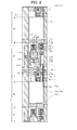
- FIG. 2 is a plan view illustrating a part of a display region of the organic electroluminescent device according to an embodiment of the present invention
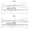
- FIG. 3 is a cross-sectional view taken along line III-III of FIG. 2
- element region DA a region where the switching TFT, the driving TFT, and an auxiliary driving TFT are formed in each pixel region
- element region DA a region where the switching TFT, the driving TFT, and an auxiliary driving TFT are formed in each pixel region
- element region DA a region where the organic light emitting diode E is formed
- EA light emission region
- the pixel region P at the upper portion is referred to as first pixel region P1
- second pixel region P2 the pixel region P at the lower portion
- the pixel region P of the organic electroluminescent device 101 has the three TFTs i.e., the switching TFT Tr1, the driving TFT Tr2, and the auxiliary driving TFT Tr3.
- the pixel region P has at least two TFTs i.e., the switching TFT Tr1 and the driving TFT Tr2, or the switching and driving TFTs Tr1 and Tr2, and at least two auxiliary driving TFTs.
- the organic electroluminescent device 101 includes a first substrate 110 having the switching and driving TFTs Tr1 and Tr2 and the organic light emitting diode E thereon, and a second substrate (not shown) for encapsulating the pixels including the organic light emitting diode E.
- the second substrate may be replaced with a film, an inorganic insulating layer, or an organic insulating layer.
- the gate line GL and the data line DL are formed crossing each other.
- a first auxiliary line AL1 is formed in parallel with the gate line GL, and a power line PL and a second auxiliary line (not shown) are formed in parallel with the data line DL.
- a region surrounded by the data line DL, the power line PL, and the first auxiliary line AL1 is the pixel region P.
- the gate line GL is located at a boundary portion between the element region DA and the light emission region EA.
- the positions of the gate line GL and the first auxiliary line AL1 may change, and in this case, a region surrounded by the data line DL, the power line PL, and the gate line GL may be the pixel region P.
- the switching TFT Tr1 is connected to the gate and data lines GL and DL
- the driving TFT Tr2 is connected to the switching TFT Tr2 and the power line PL
- the auxiliary driving TFT Tr3 is connected to the driving TFT Tr2.
- the first auxiliary line AL1 and the second auxiliary line are in the element region DA.
- the first auxiliary line AL1 is connected to a gate electrode of the auxiliary driving TFT Tr3, and the second auxiliary line is electrically connected to a source electrode 133c of the auxiliary driving TFT Tr3 via a first auxiliary pattern APn1.
- the source electrode 133b of the driving TFT Tr2 is connected to the power line PL
- the drain electrode 136b of the driving TFT Tr2 is connected to a drain electrode 136c of the auxiliary driving TFT Tr3 and a first portion 160a of a first electrode 160
- the gate electrode 115b of the driving TFT Tr2 is connected to a drain electrode 136a of the switching TFT Tr1.
- the first auxiliary line AL1 may have the function similar to the gate line GL applying a scan voltage to a gate electrode 115a of the switching TFT Tr1, and particularly, may function as a sense line that applies a sense voltage to the gate electrode 115c of the auxiliary driving TFT Tr3.
- the second auxiliary line functions as a reference line that applies a common voltage as a reference voltage.
- the first electrode 160 contacts the drain electrode 136b of the driving TFT Tr2 via a second drain contact hole 153, and extends from the element region DA to the light emission region EA.
- the first electrode 160 as a characteristic component of the embodiment includes three portions i.e., the first portion 160a, a second portion 160b, and a third portion 160c.
- the first portion 160a of the first electrode 160 is located at the element region DA and contacts the drain electrode 136b of the driving TFT Tr2.
- the second portion 160b is located at the light emission region EA and functions as one part of the organic light emitting diode E.
- the third portion 160c of the first electrode 160 corresponding to a pixel region is located at a neighboring pixel region.
- the third portion 160c of the first electrode 160, the first and second portions 160a and 160b of which are formed at the second pixel region P2 is located at the element region DA of the upper neighboring pixel region i.e., the first pixel region P1.
- an end of the third portion 160c of the first electrode 160 belonging to the second pixel region P2 overlaps the drain electrode 136b of the driving TFT Tr2 of the first pixel region P1.
- the first electrode 160 having the above-described structure, even if the driving TFT Tr2 is defective and the pixel region P1 having such the driving TFT Tr2 becomes a bright spot or dark spot, a repair process may be conducted such that the third portion 160c of the first electrode 160 contacts the drain electrode 136b of the driving TFT Tr2 of the neighboring pixel region P2. Thus the defective pixel region P1 can be operated normally.
- a bank 163 may be formed at a boundary portion between neighboring pixel regions P and the element region DA of each pixel region P.
- An organic light emitting layer 165 may be formed on the first electrode 160 corresponding to the light emission region EA surrounded by the bank 163.
- a second electrode 168 may be formed on the bank 163 and the organic light emitting layer 165. The second electrode 168 may be formed substantially all over the display region.
- the first electrode 160, the organic light emitting layer 163, and the second electrode 163 form the organic light emitting diode E.
- the organic light emitting layer 163 is formed in the light emission region EA. However, it should be understood that the organic light emitting layer 163 may be formed substantially all over that the display region.
- the third portion 160c of the first electrode 160 of each pixel region overlaps the driving TFT Tr2 at the upper neighboring pixel region.
- the third portion 160c of the first electrode 160 of each pixel region may overlap the driving TFT Tr2 at the lower neighboring pixel region.
- the pixel regions P on each column line along the extension direction of the data line DL emit the same color, and at least three neighboring pixel regions P on each row line along the extension direction of the gate line GL emit different colors.
- the pixel regions P on each column line connected to the same data line DL emit the same color
- red, green, and blue pixel regions, or red, green, blue, and white pixel regions on each row line connected to the same gate line GL are neighboring and repeated along each row line.
- the third portion 160c of the first electrode 160 of the neighboring pixel region P can be electrically connected to the drain electrode of the driving TFT Tr2 of the defective pixel region P. repair process,
- the defective pixel region P can be operated identically to the neighboring pixel region. Therefore, the defective pixel region P can be operated to have the same color and brightness as the upper or lower neighboring pixel region P. Therefore, the image display can be performed almost identically to an image display when there are no defective pixel regions.
- the switching TFT Tr1, the driving TFT Tr2, and the auxiliary driving TFT Tr3 have substantially the same cross-sectional structure, the structure of such the TFTs is explained with the driving TFT Tr2. Further, characters, "a”, “b” and “c” are affixed to the end of the numerals of the gate electrodes 133, the oxide semiconductor layers 120, and the source and drain electrodes 133 and 136, belonging to the switching TFT Tr1, the driving TFT Tr2, and the auxiliary driving TFT Tr3, respectively.
- the driving TFT Tr2 includes the gate electrode 115b, the gate insulating layer 118, the oxide semiconductor layer 120b, the etch stopper 123 having the semiconductor contact hole 125, and the source and drain electrodes 133b and 136b which are spaced apart from each other on the etch stopper 123 and contacts the corresponding portions of the oxide semiconductor layer 120b via the corresponding semiconductor contact holes 125.
- the first auxiliary line AL1 may be formed at the same layer and of the same material as the gate electrode 115b of the driving TFT Tr2, and extends along and is spaced apart from the extension direction of the gate line GL.
- the data line DL may be formed at the same layer and of the same material as the source and drain electrodes 133b and 136b of the driving TFT Tr2, and crosses the gate line GL.
- the second auxiliary line may be spaced apart from and parallel with the data line DL.
- the gate electrode 115a of the switching TFT Tr1 may be connected to the gate line GL, and the source electrode 133a of the switching TFT Tr1 may be connected to the data line DL.
- a portion of the first auxiliary line AL1 functions as the gate electrode 115c of the auxiliary driving TFT Tr3.
- the second auxiliary line may be connected to the source electrode 133c of the auxiliary driving TFT Tr3 through the auxiliary pattern 117.
- the power line PL may be connected to the source electrode 133b of the driving TFT Tr2.
- the switching TFT Tr1, the driving TFT Tr2, and the auxiliary driving TFT Tr3 are formed in a bottom gate type.
- the switching TFT Tr1, the driving TFT Tr2, and the auxiliary driving TFT Tr3 may be formed in other type.
- the switching TFT Tr1, the driving TFT Tr2, and the auxiliary driving TFT Tr3 may be formed in a co-planar type using a polysilicon semiconductor.
- the TFTs Tr1 to Tr3 each include a semiconductor layer, which has an active region made of intrinsic polysilicon and source and drain regions at both sides of the active region made of impurity-doped polysilicon, a gate insulating layer, a gate electrode corresponding to the active region, an inter-layered insulating layer having semiconductor contact holes exposing the source and drain regions, respectively, and source and drain electrodes contacting the source and drain electrodes through the semiconductor contact holes, respectively.
- the co-planar type TFT further includes the inter-layered insulating layer compared with the bottom gate type TFT.
- the gate line and the first auxiliary line may be formed on the gate insulating layer, and the data line, the power line and the second auxiliary line formed on the inter-layered insulating layer.
- the power line PL may be formed at the same layer as the data line DL or the gate line.
- the gate electrode 115b, the gate line GL, the data line DL, the power line PL, the source and drain electrodes 133b and 136b, the first auxiliary line AL1, and the second auxiliary line may be each formed with a single-layered or multiple-layered structure using at least one low-resistance metal material at least one of copper (Cu), copper alloy, aluminum (Al), aluminum alloy (AlNd), molybdenum (Mo), and molybdenum alloy (e.g., MoTi).
- Cu copper
- Al aluminum
- AlNd aluminum alloy
- Mo molybdenum
- MoTi molybdenum alloy
- a passivation layer 140 may be formed on the switching TFT Tr1, the driving TFT Tr2, and the auxiliary driving TFT Tr3, and may be made of an inorganic insulating material, for example, silicon oxide (SiO 2 ) or silicon nitride (SiNx).
- the passivation layer 140 may include a first drain contact hole 143 exposing the drain electrode of the driving TFT Tr2.
- a light shielding pattern 145 may be formed on the passivation layer 140 corresponding to the driving TFT Tr2 in each element region DA.
- the light shielding pattern 145 may contact the drain electrode 136b of the driving TFT Tr2 via the first drain contact hole 143.
- the light shielding pattern 145 may be configured to substantially shield the entire separate region between the source and drain electrodes 133b and 136b; and thus, light incidence through the separate region between the source and drain electrodes 133b and 136b can be prevented.
- the light shielding pattern 145 functions to block light incident on the oxide semiconductor layer 120b through the separate region between the source and drain electrodes 133b and 136b and prevent malfunction of the driving TFT Tr2 due to leakage current caused by energy absorbed from incident light.
- the light shielding pattern may be formed of an opaque metal material having low resistance and light-shielding property.
- the light shielding pattern is formed corresponding to the driving TFT Tr2.
- the light shielding pattern 145 may also be formed on the passivation layer 140 over the switching TFT Tr1 and the auxiliary driving TFT Tr3.
- the gate electrode 115b and the drain electrode 136b overlap each other with the gate insulating layer 118 and the etch stopper 123 therebetween at a region where the oxide semiconductor layer 120b is not formed to form the storage capacitor StgC.
- the storage capacitor StgC may be formed at the driving TFT Tr2 but not formed at the switching TFT Tr1 and the auxiliary driving TFT Tr3.
- a planarization layer 150 may be formed on the light shielding pattern 145 to cover the display region and having a substantially flat surface.
- the planarization layer 150 may include a second drain contact hole 153 which exposes a portion of the light shielding pattern 145 contacting the drain electrode 136b.
- the second drain contact hole 153 may overlap the first drain contact hole 143 in order to reduce the area of the element region DA.
- the planarization layer 150 may have a welding hole wdh at a portion of the drain electrode 136b of the pixel region P1 where an end of the third portion 160c of the first electrode 160 of the pixel region P2 is located.
- the light shielding pattern 145 is not formed at the region where the welding hole wdh is formed, and the welding hole wdh exposes a portion of the passivation layer 140 therebelow.
- the first electrode 160 may be formed on the planarization layer 150, and can be connected to the light shielding pattern 145, which is connected to the drain electrode 136b, through the second drain contact hole 153.
- the first electrode 160 may be made of a transparent conductive material having a high work function, for example, indium-tin-oxide (ITO) and function as an anode.
- ITO indium-tin-oxide
- the first electrode 160 includes the first to third portions 160a, 160b and 160c.
- the passivation layer 140 may have a drain contact hole, which may be formed at the same position and at the same shape as the first drain contact hole 143, the planarization 150 may be not employed, and the first electrode 160 may directly contact the drain electrode 136b through the drain contact hole.
- the second portion 160b of the first electrode 160 may be located at the light emission region EA of each pixel region P.
- the first portion 160a of the first electrode 160 extends from an end of the second portion 160b and is located at the element region DA of the pixel region P.
- the third portion 160c of the first electrode 160 extends from the other end of the second portion 160b to the element region DA of the neighboring pixel region P1 so that the third portion 160c overlaps the drain electrode 136b of the driving TFT Tr2 of the neighboring pixel region P1.
- the third portion 160c of the first electrode 160 is on the passivation layer 140 and in the welding hole wdh.
- the bank 163 may be formed on the first electrode 160 and at the boundary of each light emission region DA.
- the bank 163 may be configured to surround each light emission region EA, overlap an edge of the second portion 160b, and expose a center portion of the first electrode 160.
- the bank 163 may be formed substantially all over each element region DA.
- the bank may be formed of an organic insulating material, for example, polyimide, or a black material, for example, black resin.
- the organic light emitting layer 165 may be formed on the second portion 160b of the first electrode 160 at the light emission region EA of each pixel region P surrounded by the bank 163.
- the second electrode 168 may be formed on the organic light emitting layer 165 and the bank 163.
- the second electrode 168 may be formed all over the display region, or be formed in a plate shape in the display region with an opening surrounded by an electrode pattern.
- the second electrode 168 may function as a cathode and may be made of a metal material having a low work function, for example, at least one of aluminum (Al), aluminum alloy (e.g., AlNd or AlMg), silver (Ag), magnesium (Mg), and gold (Au).
- the openings may be formed at a portion of each element region DA where the driving TFT Tr2 and the third portion 160c of the first electrode 160 overlap each other. This is for easily conducting a repair process when the pixel region P has a dark defect or bright defect.
- the second electrode 168 may be not required to have an opening, and forming the second electrode 168 all over the display region without openings is not problematic.
- the first and second electrodes 160 and 168 and the organic light emitting layer 165 may form the organic light emitting diode E.
- a first light emitting compensation layer may be formed between the first electrode 160 and the light emitting layer 165, and a second light emitting compensation layer may be formed between the second electrode 168 and the light emitting layer 165.
- Each of the first and second light emitting compensation layers may have a multiple-layered structure so as to improve light emission efficiency.
- the multiple-layered first light emitting compensation layer may include a hole injection layer and a hole transporting layer sequentially formed on the first electrode 160, and the multiple-layered second light emitting compensation layer may include an electron transporting layer and an electron injection layer sequentially formed on the organic light emitting layer 165.
- the first and second light emitting compensation layer may each have a single-layered structure.
- the single-layered first light emitting compensation layer may have one of the hole injection layer and the hole transporting layer, and the single-layered first light emitting compensation layer may have one of the electron injection layer and the electron transporting layer.
- the first light emitting compensation layer may include an electron blocking layer
- the second light emitting compensation layer may include a hole blocking layer
- red, green and blue color filter patterns may be formed between the passivation layer 140 and the planarization layer 150 in the light emission regions EA of the respectively pixel regions P.
- the organic light emitting layer 165 of each pixel region P is a white organic light emitting layer emitting white.
- the white emitted from the organic light emitting layers passes through the respective color filter patterns and is changed into the respective colors so that full color can be displayed.
- the organic electroluminescent device 101 uses four colors, red, green, blue, and white. Thus, contrast ratio and brightness can be improved.
- the organic electroluminescent device 101 may not use the color filter patterns.
- red, green, and blue organic light emitting layers may be formed in the respective pixel regions, or red, green, blue, and white light emitting layers may be formed in the respective pixel regions.
- the organic electroluminescent device 101 may include a second substrate which faces the first substrate 110 having the above-described configuration and functions to encapsulate the organic light emitting diode E.
- an adhesive may be formed between peripheral portions of the first substrate 110 and the second substrate to attach the first and second substrates to manufacture a display panel.
- a space between the first substrate 110 and the second substrate may be in a vacuum or be filled with an inert gas.
- the second substrate for encapsulation may be made of plastic having a flexible property, or glass.
- the organic electroluminescent device 101 may not use the second substrate.
- a film having an adhesive layer may be attached to the first substrate 110 such that the film contacts the second electrode 168, and further, an organic insulating layer or inorganic insulating layer as a capping layer may be formed on the second electrode 168.
- an organic insulating layer or inorganic insulating layer as a capping layer may be formed on the second electrode 168, and function as an encapsulation layer instead of the second substrate.
- the organic electroluminescent device 101 because of the first electrode 160 configuration as described above, a pixel region P having a dark or bright defect can be repaired to be operated normally. Accordingly, an error rate and failure cost can be reduced, and further non-defective or error-minimized display devices can be provided.
- FIG. 5 is a plan view illustrating a laser-cut portion and a welding portion for repair of the organic electroluminescent device according to the embodiment of the present invention.
- FIGs. 6 and 7 are cross-sectional views taken along a line VI-VI of FIG. 5 showing the organic electroluminescent device before the laser-cut process and after the laser-cut process, respectively.
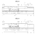
- FIGs. 8 and 9 are cross-sectional views of the organic electroluminescent devices after the welding process according to the embodiment and the alternative embodiment of the present invention, respectively.
- FIGs. 8 and 9 correspond to FIGs. 3 and 4 , respectively.
- the switching TFT Tr1, the driving TFT Tr2, or the auxiliary driving TFT Tr3 of a certain pixel region P and the pixel region P becomes a dark spot or bright spot, in order to disconnect the electrical connections among the TFTs Tr1 to Tr3, the connection portions among the TFTs Tr1 to Tr3 and the connection portion between the power line PL and the driving TFT Tr2 are cut.
- the organic electroluminescent device of the embodiments has three TFTs Tr1 to Tr3 in each pixel region P, and thus a number of the cut portions can be three. However, in case that two TFTs are formed in each pixel region, a number of the cut portions can be two. The number of the cut portions can be the same as a number of the TFTs.
- connection portion between the switching TFT and the driving TFT and the connection portion between the driving TFT and the power line may be cut.
- connection portions may be cut, for example, using a laser cutting process. Accordingly, each of the connection portions may be completely cut and separated.
- a welding process is performed using a laser apparatus.
- the welding process is performed for the defective pixel region P1 i.e., the first pixel region P1.
- the third portion 160c of the first electrode of the neighboring pixel region P2 i.e., the second pixel region P2, that is not defective, is laser-irradiated to be welded to and electrically connected to the drain electrode 136b of the driving TFT Tr2 of the defective first pixel region P1.
- the light shielding pattern 145 connected to the drain electrode 136b of the driving TFT Tr2 contacts the third portion 160c of the first electrode 160 in the welding process so that the drain electrode 136b of the driving TFT Tr2 of the defective first pixel region P1 is electrically connected to the first electrode 160 of the second pixel region P2.
- the drain electrode 136b of the driving TFT Tr2 contacts the third portion 160c of the first electrode 160 in the welding process.
- the defective pixel region P1 can be operated by the driving TFT Tr2 of the neighboring pixel region P2.
- a signal applied to the first electrode 160 of the second pixel region P2 is supplied to the first electrode 160 of the first pixel region P1 through the drain electrode 136b of the first pixel region P1 connected to the first electrode 160 of the second pixel region P2 by the welding process.
- the defective first pixel region P1 can be operated identically to the second pixel region P2.
- a dark-spot or bright-spot defective pixel region P1 can become a normally operated pixel region.
- the defective pixel region can be normally operated after the repair method, a non-defective or error-minimized display device can be provided. Moreover, error rate and failure costs can be reduced, and thus, production costs can be reduced.
Landscapes
- Engineering & Computer Science (AREA)
- Microelectronics & Electronic Packaging (AREA)
- Physics & Mathematics (AREA)
- Geometry (AREA)
- Optics & Photonics (AREA)
- Manufacturing & Machinery (AREA)
- Plasma & Fusion (AREA)
- Mechanical Engineering (AREA)
- Electroluminescent Light Sources (AREA)
- Devices For Indicating Variable Information By Combining Individual Elements (AREA)
Applications Claiming Priority (1)
| Application Number | Priority Date | Filing Date | Title |
|---|---|---|---|
| KR1020130143732A KR102112649B1 (ko) | 2013-11-25 | 2013-11-25 | 유기전계 발광소자 및 이의 리페어 방법 |
Publications (3)
| Publication Number | Publication Date |
|---|---|
| EP2876684A2 true EP2876684A2 (fr) | 2015-05-27 |
| EP2876684A3 EP2876684A3 (fr) | 2015-06-03 |
| EP2876684B1 EP2876684B1 (fr) | 2021-01-13 |
Family
ID=51355470
Family Applications (1)
| Application Number | Title | Priority Date | Filing Date |
|---|---|---|---|
| EP14181215.6A Active EP2876684B1 (fr) | 2013-11-25 | 2014-08-18 | Dispositif électroluminescent organique et son procédé de réparation |
Country Status (4)
| Country | Link |
|---|---|
| US (2) | US9502487B2 (fr) |
| EP (1) | EP2876684B1 (fr) |
| KR (1) | KR102112649B1 (fr) |
| CN (1) | CN104659055B (fr) |
Families Citing this family (38)
| Publication number | Priority date | Publication date | Assignee | Title |
|---|---|---|---|---|
| KR102112649B1 (ko) * | 2013-11-25 | 2020-05-19 | 엘지디스플레이 주식회사 | 유기전계 발광소자 및 이의 리페어 방법 |
| KR102240894B1 (ko) * | 2014-02-26 | 2021-04-16 | 삼성디스플레이 주식회사 | 표시 장치 및 표시 장치의 제조 방법 |
| KR102222901B1 (ko) | 2014-07-07 | 2021-03-04 | 엘지디스플레이 주식회사 | 유기발광 표시장치 구동 방법 |
| CN104409656B (zh) * | 2014-11-27 | 2017-02-22 | 京东方科技集团股份有限公司 | 一种有机电致发光器件及其制备方法、显示装置 |
| CN104538421B (zh) * | 2014-12-16 | 2018-07-13 | 深圳市华星光电技术有限公司 | Oled显示基板及其制造方法 |
| KR102341352B1 (ko) * | 2015-04-08 | 2021-12-20 | 삼성디스플레이 주식회사 | 터치 센서를 포함하는 표시 장치 |
| KR102391347B1 (ko) * | 2015-04-09 | 2022-04-28 | 삼성디스플레이 주식회사 | 박막트랜지스터 어레이 기판 및 이를 구비한 디스플레이 장치 |
| KR102571667B1 (ko) * | 2015-06-30 | 2023-08-30 | 엘지디스플레이 주식회사 | 유기발광표시장치 |
| KR102402605B1 (ko) * | 2015-07-28 | 2022-05-27 | 삼성디스플레이 주식회사 | 유기 발광 표시 장치 |
| KR101795579B1 (ko) | 2015-11-10 | 2017-11-08 | 엘지디스플레이 주식회사 | 유기 발광 표시 장치 및 그 제조 방법 |
| KR102401438B1 (ko) * | 2015-11-10 | 2022-05-23 | 엘지디스플레이 주식회사 | 유기전계발광 표시장치 |
| KR102636147B1 (ko) | 2015-12-31 | 2024-02-08 | 엘지디스플레이 주식회사 | 투명표시장치 |
| KR102627067B1 (ko) * | 2016-05-11 | 2024-01-18 | 엘지디스플레이 주식회사 | 유기발광표시장치 및 그 제조방법 |
| KR102623624B1 (ko) * | 2016-05-18 | 2024-01-10 | 삼성디스플레이 주식회사 | 트랜지스터 표시판 및 그 제조 방법 |
| CN105789266A (zh) * | 2016-05-30 | 2016-07-20 | 京东方科技集团股份有限公司 | 一种oled阵列基板及其制备方法、显示装置 |
| KR102688179B1 (ko) * | 2016-05-31 | 2024-07-25 | 엘지디스플레이 주식회사 | 유기 발광 표시 장치 및 이의 리페어 방법 |
| CN106328010B (zh) | 2016-09-23 | 2019-01-04 | 歌尔科技有限公司 | 显示设备、电子设备、发光单元损坏处理方法及设备 |
| KR102568518B1 (ko) * | 2016-10-25 | 2023-08-18 | 엘지디스플레이 주식회사 | 고 개구율을 갖는 초고해상도 평판 표시장치 |
| KR102627343B1 (ko) * | 2016-11-30 | 2024-01-22 | 엘지디스플레이 주식회사 | 표시장치 |
| CN108336107A (zh) * | 2017-01-19 | 2018-07-27 | 京东方科技集团股份有限公司 | 有机发光二极管(oled)阵列基板及其制备方法、显示装置 |
| CN107204356B (zh) * | 2017-06-22 | 2020-11-03 | 昆山国显光电有限公司 | 电致发光装置及其制备方法 |
| CN107221287B (zh) * | 2017-07-31 | 2019-09-06 | 京东方科技集团股份有限公司 | 显示面板及其像素修复装置、像素修复方法和显示器 |
| CN207134356U (zh) * | 2017-09-04 | 2018-03-23 | 京东方科技集团股份有限公司 | 一种阵列基板及显示装置 |
| CN110165058A (zh) * | 2018-03-26 | 2019-08-23 | 京东方科技集团股份有限公司 | 阵列基板及其制备方法、修复方法、显示装置 |
| CN109599427B (zh) | 2018-12-14 | 2021-05-14 | 京东方科技集团股份有限公司 | 显示基板的制备方法、显示面板及显示装置 |
| KR102719960B1 (ko) | 2018-12-27 | 2024-10-18 | 엘지디스플레이 주식회사 | 유기발광 표시장치 |
| CN113474908A (zh) * | 2019-04-26 | 2021-10-01 | 松下知识产权经营株式会社 | 摄像元件 |
| JP7599156B2 (ja) | 2019-04-26 | 2024-12-13 | パナソニックIpマネジメント株式会社 | 撮像素子 |
| JP7664528B2 (ja) | 2019-04-26 | 2025-04-18 | パナソニックIpマネジメント株式会社 | 撮像素子 |
| KR102732988B1 (ko) * | 2019-09-02 | 2024-11-20 | 엘지디스플레이 주식회사 | 투명 표시장치 |
| CN110797351B (zh) * | 2019-11-08 | 2022-05-20 | 京东方科技集团股份有限公司 | 一种阵列基板、其检测方法、显示面板及显示装置 |
| KR102723489B1 (ko) * | 2019-12-27 | 2024-10-28 | 엘지디스플레이 주식회사 | 유기 발광 표시 장치 |
| TWI740484B (zh) * | 2020-05-04 | 2021-09-21 | 宏碁股份有限公司 | 顯示裝置與其製造方法 |
| CN113972197A (zh) * | 2020-07-23 | 2022-01-25 | 宏碁股份有限公司 | 显示装置与其制造方法 |
| CN114005855B (zh) * | 2021-09-28 | 2022-07-22 | 惠科股份有限公司 | 阵列基板、显示面板及面板坏点修复方法 |
| KR102874688B1 (ko) * | 2021-12-16 | 2025-10-22 | 삼성디스플레이 주식회사 | 표시 장치 및 그 제조 방법 |
| KR102904517B1 (ko) | 2021-12-23 | 2025-12-24 | 엘지디스플레이 주식회사 | 리페어 구조를 갖는 전계 발광 표시장치 및 그 제조 방법 |
| CN114784076B (zh) * | 2022-04-27 | 2025-08-26 | 深圳市华星光电半导体显示技术有限公司 | 显示面板和显示面板的修复方法 |
Family Cites Families (22)
| Publication number | Priority date | Publication date | Assignee | Title |
|---|---|---|---|---|
| US6853052B2 (en) * | 2002-03-26 | 2005-02-08 | Semiconductor Energy Laboratory Co., Ltd. | Semiconductor device having a buffer layer against stress |
| KR101152134B1 (ko) * | 2005-08-26 | 2012-06-15 | 삼성전자주식회사 | 유기 발광 표시 장치 및 그 제조 방법 |
| KR100720142B1 (ko) * | 2005-11-25 | 2007-05-18 | 삼성전자주식회사 | 표시 장치와 표시장치의 제조방법 |
| KR100688971B1 (ko) * | 2006-02-16 | 2007-03-08 | 삼성전자주식회사 | 디스플레이장치 |
| JP4415971B2 (ja) * | 2006-05-10 | 2010-02-17 | カシオ計算機株式会社 | 表示装置及びその製造方法 |
| KR101293565B1 (ko) * | 2007-01-26 | 2013-08-06 | 삼성디스플레이 주식회사 | 유기 발광 표시 장치 및 그 제조 방법 |
| KR100853540B1 (ko) * | 2007-02-01 | 2008-08-21 | 삼성에스디아이 주식회사 | 유기전계발광표시장치 및 그의 에이징 방법 |
| JP4356899B2 (ja) * | 2007-03-15 | 2009-11-04 | 財団法人山形県産業技術振興機構 | 有機el発光装置およびその製造方法 |
| JP5024529B2 (ja) * | 2007-04-12 | 2012-09-12 | ソニー株式会社 | 表示装置の製造方法およびtftアレイ基板の製造方法 |
| JP2009071289A (ja) * | 2007-08-17 | 2009-04-02 | Semiconductor Energy Lab Co Ltd | 半導体装置およびその作製方法 |
| JP5184042B2 (ja) * | 2007-10-17 | 2013-04-17 | グローバル・オーエルイーディー・テクノロジー・リミテッド・ライアビリティ・カンパニー | 画素回路 |
| GB0807767D0 (en) * | 2008-04-29 | 2008-06-04 | Plastic Logic Ltd | Off-set top pixel electrode configuration |
| KR20100009385A (ko) * | 2008-07-18 | 2010-01-27 | 삼성전자주식회사 | 박막 트랜지스터 및 그 제조 방법 |
| KR101659935B1 (ko) * | 2008-12-01 | 2016-09-27 | 삼성디스플레이 주식회사 | 유기 발광 소자 및 이를 포함하는 유기 발광 표시 장치 |
| KR20120051727A (ko) * | 2009-07-31 | 2012-05-22 | 가부시키가이샤 한도오따이 에네루기 켄큐쇼 | 반도체 디바이스 및 그 형성 방법 |
| KR101698543B1 (ko) * | 2009-11-19 | 2017-01-23 | 엘지디스플레이 주식회사 | 유기 발광소자 및 그 제조방법 |
| KR20110097121A (ko) * | 2010-02-24 | 2011-08-31 | 엘지디스플레이 주식회사 | 어레이 기판 |
| GB2489939A (en) * | 2011-04-11 | 2012-10-17 | Plastic Logic Ltd | Control of capacitive coupling in pixel circuitry |
| JP2013012610A (ja) * | 2011-06-29 | 2013-01-17 | Dainippon Printing Co Ltd | 薄膜トランジスタおよびその製造方法 |
| KR101830179B1 (ko) * | 2011-11-03 | 2018-02-21 | 삼성디스플레이 주식회사 | 유기 전계 발광 표시 장치 |
| KR101339000B1 (ko) * | 2011-12-14 | 2013-12-09 | 엘지디스플레이 주식회사 | 유기전계발광 표시소자 및 그 제조방법 |
| KR102112649B1 (ko) * | 2013-11-25 | 2020-05-19 | 엘지디스플레이 주식회사 | 유기전계 발광소자 및 이의 리페어 방법 |
-
2013
- 2013-11-25 KR KR1020130143732A patent/KR102112649B1/ko active Active
-
2014
- 2014-08-18 EP EP14181215.6A patent/EP2876684B1/fr active Active
- 2014-08-19 US US14/463,175 patent/US9502487B2/en active Active
- 2014-10-15 CN CN201410543420.4A patent/CN104659055B/zh active Active
-
2016
- 2016-10-14 US US15/294,222 patent/US9761644B2/en active Active
Non-Patent Citations (1)
| Title |
|---|
| None |
Also Published As
| Publication number | Publication date |
|---|---|
| EP2876684B1 (fr) | 2021-01-13 |
| US9761644B2 (en) | 2017-09-12 |
| US9502487B2 (en) | 2016-11-22 |
| CN104659055A (zh) | 2015-05-27 |
| US20170033168A1 (en) | 2017-02-02 |
| KR102112649B1 (ko) | 2020-05-19 |
| CN104659055B (zh) | 2017-11-17 |
| KR20150059949A (ko) | 2015-06-03 |
| EP2876684A3 (fr) | 2015-06-03 |
| US20150144904A1 (en) | 2015-05-28 |
Similar Documents
| Publication | Publication Date | Title |
|---|---|---|
| US9761644B2 (en) | Organic electroluminescent device and repairing method thereof | |
| CN108269831B (zh) | 具有连接包层电极的有机发光显示装置 | |
| US10249700B2 (en) | OLED array substrate, display apparatus and method for repairing dark spot thereon | |
| US20060279499A1 (en) | Organic light-emitting device | |
| CN113193025A (zh) | 显示面板及显示装置 | |
| US11871627B2 (en) | Display device having a lower pattern overlapping an active pattern | |
| KR101286094B1 (ko) | 유기전계발광소자의 제조 방법 및 수리방법 | |
| KR20050067680A (ko) | 듀얼패널타입 유기전계발광 소자 및 그 제조방법 | |
| US20230200169A1 (en) | Electroluminescence Display | |
| US9153632B2 (en) | Organic light emitting device display and manufacturing method thereof | |
| US12389756B2 (en) | Organic light emitting diode display device and method of fabricating the same | |
| US11908358B2 (en) | Gate test part and display device including the same | |
| US20240260354A1 (en) | Display panel and display device | |
| JP2010249883A (ja) | 画像表示装置及びその修正方法 | |
| CN117320512A (zh) | 发光显示设备 | |
| CN221510183U (zh) | 显示装置 | |
| US20260075705A1 (en) | Mother board for display device and display device | |
| US20250212634A1 (en) | Display device | |
| US20250212619A1 (en) | Display apparatus | |
| US20260068459A1 (en) | Display device | |
| KR20250103233A (ko) | 표시 장치 | |
| CN120239495A (zh) | 透明显示装置 | |
| KR20090123565A (ko) | 유기발광다이오드 표시장치 및 이의 제조 방법 |
Legal Events
| Date | Code | Title | Description |
|---|---|---|---|
| PUAL | Search report despatched |
Free format text: ORIGINAL CODE: 0009013 |
|
| PUAI | Public reference made under article 153(3) epc to a published international application that has entered the european phase |
Free format text: ORIGINAL CODE: 0009012 |
|
| 17P | Request for examination filed |
Effective date: 20140818 |
|
| AK | Designated contracting states |
Kind code of ref document: A2 Designated state(s): AL AT BE BG CH CY CZ DE DK EE ES FI FR GB GR HR HU IE IS IT LI LT LU LV MC MK MT NL NO PL PT RO RS SE SI SK SM TR |
|
| AX | Request for extension of the european patent |
Extension state: BA ME |
|
| AK | Designated contracting states |
Kind code of ref document: A3 Designated state(s): AL AT BE BG CH CY CZ DE DK EE ES FI FR GB GR HR HU IE IS IT LI LT LU LV MC MK MT NL NO PL PT RO RS SE SI SK SM TR |
|
| AX | Request for extension of the european patent |
Extension state: BA ME |
|
| RIC1 | Information provided on ipc code assigned before grant |
Ipc: H01L 27/32 20060101AFI20150429BHEP Ipc: H01L 51/52 20060101ALI20150429BHEP |
|
| R17P | Request for examination filed (corrected) |
Effective date: 20150804 |
|
| RBV | Designated contracting states (corrected) |
Designated state(s): AL AT BE BG CH CY CZ DE DK EE ES FI FR GB GR HR HU IE IS IT LI LT LU LV MC MK MT NL NO PL PT RO RS SE SI SK SM TR |
|
| STAA | Information on the status of an ep patent application or granted ep patent |
Free format text: STATUS: EXAMINATION IS IN PROGRESS |
|
| 17Q | First examination report despatched |
Effective date: 20180702 |
|
| RIC1 | Information provided on ipc code assigned before grant |
Ipc: H01L 51/52 20060101ALI20200331BHEP Ipc: H01L 27/32 20060101AFI20200331BHEP Ipc: H01L 51/56 20060101ALI20200331BHEP |
|
| GRAP | Despatch of communication of intention to grant a patent |
Free format text: ORIGINAL CODE: EPIDOSNIGR1 |
|
| STAA | Information on the status of an ep patent application or granted ep patent |
Free format text: STATUS: GRANT OF PATENT IS INTENDED |
|
| INTG | Intention to grant announced |
Effective date: 20200821 |
|
| RAP1 | Party data changed (applicant data changed or rights of an application transferred) |
Owner name: LG DISPLAY CO., LTD. |
|
| GRAS | Grant fee paid |
Free format text: ORIGINAL CODE: EPIDOSNIGR3 |
|
| GRAA | (expected) grant |
Free format text: ORIGINAL CODE: 0009210 |
|
| STAA | Information on the status of an ep patent application or granted ep patent |
Free format text: STATUS: THE PATENT HAS BEEN GRANTED |
|
| AK | Designated contracting states |
Kind code of ref document: B1 Designated state(s): AL AT BE BG CH CY CZ DE DK EE ES FI FR GB GR HR HU IE IS IT LI LT LU LV MC MK MT NL NO PL PT RO RS SE SI SK SM TR |
|
| REG | Reference to a national code |
Ref country code: GB Ref legal event code: FG4D |
|
| REG | Reference to a national code |
Ref country code: CH Ref legal event code: EP |
|
| REG | Reference to a national code |
Ref country code: DE Ref legal event code: R096 Ref document number: 602014074176 Country of ref document: DE |
|
| REG | Reference to a national code |
Ref country code: IE Ref legal event code: FG4D |
|
| REG | Reference to a national code |
Ref country code: AT Ref legal event code: REF Ref document number: 1355189 Country of ref document: AT Kind code of ref document: T Effective date: 20210215 |
|
| REG | Reference to a national code |
Ref country code: AT Ref legal event code: MK05 Ref document number: 1355189 Country of ref document: AT Kind code of ref document: T Effective date: 20210113 |
|
| REG | Reference to a national code |
Ref country code: NL Ref legal event code: MP Effective date: 20210113 |
|
| REG | Reference to a national code |
Ref country code: LT Ref legal event code: MG9D |
|
| PG25 | Lapsed in a contracting state [announced via postgrant information from national office to epo] |
Ref country code: LT Free format text: LAPSE BECAUSE OF FAILURE TO SUBMIT A TRANSLATION OF THE DESCRIPTION OR TO PAY THE FEE WITHIN THE PRESCRIBED TIME-LIMIT Effective date: 20210113 Ref country code: PT Free format text: LAPSE BECAUSE OF FAILURE TO SUBMIT A TRANSLATION OF THE DESCRIPTION OR TO PAY THE FEE WITHIN THE PRESCRIBED TIME-LIMIT Effective date: 20210513 Ref country code: HR Free format text: LAPSE BECAUSE OF FAILURE TO SUBMIT A TRANSLATION OF THE DESCRIPTION OR TO PAY THE FEE WITHIN THE PRESCRIBED TIME-LIMIT Effective date: 20210113 Ref country code: GR Free format text: LAPSE BECAUSE OF FAILURE TO SUBMIT A TRANSLATION OF THE DESCRIPTION OR TO PAY THE FEE WITHIN THE PRESCRIBED TIME-LIMIT Effective date: 20210414 Ref country code: FI Free format text: LAPSE BECAUSE OF FAILURE TO SUBMIT A TRANSLATION OF THE DESCRIPTION OR TO PAY THE FEE WITHIN THE PRESCRIBED TIME-LIMIT Effective date: 20210113 Ref country code: BG Free format text: LAPSE BECAUSE OF FAILURE TO SUBMIT A TRANSLATION OF THE DESCRIPTION OR TO PAY THE FEE WITHIN THE PRESCRIBED TIME-LIMIT Effective date: 20210413 Ref country code: NO Free format text: LAPSE BECAUSE OF FAILURE TO SUBMIT A TRANSLATION OF THE DESCRIPTION OR TO PAY THE FEE WITHIN THE PRESCRIBED TIME-LIMIT Effective date: 20210413 Ref country code: NL Free format text: LAPSE BECAUSE OF FAILURE TO SUBMIT A TRANSLATION OF THE DESCRIPTION OR TO PAY THE FEE WITHIN THE PRESCRIBED TIME-LIMIT Effective date: 20210113 |
|
| PG25 | Lapsed in a contracting state [announced via postgrant information from national office to epo] |
Ref country code: AT Free format text: LAPSE BECAUSE OF FAILURE TO SUBMIT A TRANSLATION OF THE DESCRIPTION OR TO PAY THE FEE WITHIN THE PRESCRIBED TIME-LIMIT Effective date: 20210113 Ref country code: PL Free format text: LAPSE BECAUSE OF FAILURE TO SUBMIT A TRANSLATION OF THE DESCRIPTION OR TO PAY THE FEE WITHIN THE PRESCRIBED TIME-LIMIT Effective date: 20210113 Ref country code: LV Free format text: LAPSE BECAUSE OF FAILURE TO SUBMIT A TRANSLATION OF THE DESCRIPTION OR TO PAY THE FEE WITHIN THE PRESCRIBED TIME-LIMIT Effective date: 20210113 Ref country code: RS Free format text: LAPSE BECAUSE OF FAILURE TO SUBMIT A TRANSLATION OF THE DESCRIPTION OR TO PAY THE FEE WITHIN THE PRESCRIBED TIME-LIMIT Effective date: 20210113 Ref country code: SE Free format text: LAPSE BECAUSE OF FAILURE TO SUBMIT A TRANSLATION OF THE DESCRIPTION OR TO PAY THE FEE WITHIN THE PRESCRIBED TIME-LIMIT Effective date: 20210113 |
|
| PG25 | Lapsed in a contracting state [announced via postgrant information from national office to epo] |
Ref country code: IS Free format text: LAPSE BECAUSE OF FAILURE TO SUBMIT A TRANSLATION OF THE DESCRIPTION OR TO PAY THE FEE WITHIN THE PRESCRIBED TIME-LIMIT Effective date: 20210513 |
|
| REG | Reference to a national code |
Ref country code: DE Ref legal event code: R097 Ref document number: 602014074176 Country of ref document: DE |
|
| PG25 | Lapsed in a contracting state [announced via postgrant information from national office to epo] |
Ref country code: CZ Free format text: LAPSE BECAUSE OF FAILURE TO SUBMIT A TRANSLATION OF THE DESCRIPTION OR TO PAY THE FEE WITHIN THE PRESCRIBED TIME-LIMIT Effective date: 20210113 Ref country code: EE Free format text: LAPSE BECAUSE OF FAILURE TO SUBMIT A TRANSLATION OF THE DESCRIPTION OR TO PAY THE FEE WITHIN THE PRESCRIBED TIME-LIMIT Effective date: 20210113 Ref country code: SM Free format text: LAPSE BECAUSE OF FAILURE TO SUBMIT A TRANSLATION OF THE DESCRIPTION OR TO PAY THE FEE WITHIN THE PRESCRIBED TIME-LIMIT Effective date: 20210113 |
|
| PLBE | No opposition filed within time limit |
Free format text: ORIGINAL CODE: 0009261 |
|
| STAA | Information on the status of an ep patent application or granted ep patent |
Free format text: STATUS: NO OPPOSITION FILED WITHIN TIME LIMIT |
|
| PG25 | Lapsed in a contracting state [announced via postgrant information from national office to epo] |
Ref country code: ES Free format text: LAPSE BECAUSE OF FAILURE TO SUBMIT A TRANSLATION OF THE DESCRIPTION OR TO PAY THE FEE WITHIN THE PRESCRIBED TIME-LIMIT Effective date: 20210113 Ref country code: DK Free format text: LAPSE BECAUSE OF FAILURE TO SUBMIT A TRANSLATION OF THE DESCRIPTION OR TO PAY THE FEE WITHIN THE PRESCRIBED TIME-LIMIT Effective date: 20210113 Ref country code: SK Free format text: LAPSE BECAUSE OF FAILURE TO SUBMIT A TRANSLATION OF THE DESCRIPTION OR TO PAY THE FEE WITHIN THE PRESCRIBED TIME-LIMIT Effective date: 20210113 Ref country code: RO Free format text: LAPSE BECAUSE OF FAILURE TO SUBMIT A TRANSLATION OF THE DESCRIPTION OR TO PAY THE FEE WITHIN THE PRESCRIBED TIME-LIMIT Effective date: 20210113 |
|
| 26N | No opposition filed |
Effective date: 20211014 |
|
| PG25 | Lapsed in a contracting state [announced via postgrant information from national office to epo] |
Ref country code: AL Free format text: LAPSE BECAUSE OF FAILURE TO SUBMIT A TRANSLATION OF THE DESCRIPTION OR TO PAY THE FEE WITHIN THE PRESCRIBED TIME-LIMIT Effective date: 20210113 |
|
| PG25 | Lapsed in a contracting state [announced via postgrant information from national office to epo] |
Ref country code: SI Free format text: LAPSE BECAUSE OF FAILURE TO SUBMIT A TRANSLATION OF THE DESCRIPTION OR TO PAY THE FEE WITHIN THE PRESCRIBED TIME-LIMIT Effective date: 20210113 |
|
| REG | Reference to a national code |
Ref country code: CH Ref legal event code: PL |
|
| PG25 | Lapsed in a contracting state [announced via postgrant information from national office to epo] |
Ref country code: MC Free format text: LAPSE BECAUSE OF FAILURE TO SUBMIT A TRANSLATION OF THE DESCRIPTION OR TO PAY THE FEE WITHIN THE PRESCRIBED TIME-LIMIT Effective date: 20210113 |
|
| REG | Reference to a national code |
Ref country code: BE Ref legal event code: MM Effective date: 20210831 |
|
| PG25 | Lapsed in a contracting state [announced via postgrant information from national office to epo] |
Ref country code: LI Free format text: LAPSE BECAUSE OF NON-PAYMENT OF DUE FEES Effective date: 20210831 Ref country code: IT Free format text: LAPSE BECAUSE OF FAILURE TO SUBMIT A TRANSLATION OF THE DESCRIPTION OR TO PAY THE FEE WITHIN THE PRESCRIBED TIME-LIMIT Effective date: 20210113 Ref country code: CH Free format text: LAPSE BECAUSE OF NON-PAYMENT OF DUE FEES Effective date: 20210831 |
|
| PG25 | Lapsed in a contracting state [announced via postgrant information from national office to epo] |
Ref country code: IS Free format text: LAPSE BECAUSE OF FAILURE TO SUBMIT A TRANSLATION OF THE DESCRIPTION OR TO PAY THE FEE WITHIN THE PRESCRIBED TIME-LIMIT Effective date: 20210513 Ref country code: LU Free format text: LAPSE BECAUSE OF NON-PAYMENT OF DUE FEES Effective date: 20210818 |
|
| PG25 | Lapsed in a contracting state [announced via postgrant information from national office to epo] |
Ref country code: IE Free format text: LAPSE BECAUSE OF NON-PAYMENT OF DUE FEES Effective date: 20210818 Ref country code: BE Free format text: LAPSE BECAUSE OF NON-PAYMENT OF DUE FEES Effective date: 20210831 |
|
| REG | Reference to a national code |
Ref country code: DE Ref legal event code: R079 Ref document number: 602014074176 Country of ref document: DE Free format text: PREVIOUS MAIN CLASS: H01L0027320000 Ipc: H10K0059000000 |
|
| PG25 | Lapsed in a contracting state [announced via postgrant information from national office to epo] |
Ref country code: HU Free format text: LAPSE BECAUSE OF FAILURE TO SUBMIT A TRANSLATION OF THE DESCRIPTION OR TO PAY THE FEE WITHIN THE PRESCRIBED TIME-LIMIT; INVALID AB INITIO Effective date: 20140818 |
|
| PG25 | Lapsed in a contracting state [announced via postgrant information from national office to epo] |
Ref country code: CY Free format text: LAPSE BECAUSE OF FAILURE TO SUBMIT A TRANSLATION OF THE DESCRIPTION OR TO PAY THE FEE WITHIN THE PRESCRIBED TIME-LIMIT Effective date: 20210113 |
|
| PG25 | Lapsed in a contracting state [announced via postgrant information from national office to epo] |
Ref country code: MK Free format text: LAPSE BECAUSE OF FAILURE TO SUBMIT A TRANSLATION OF THE DESCRIPTION OR TO PAY THE FEE WITHIN THE PRESCRIBED TIME-LIMIT Effective date: 20210113 |
|
| PG25 | Lapsed in a contracting state [announced via postgrant information from national office to epo] |
Ref country code: MT Free format text: LAPSE BECAUSE OF FAILURE TO SUBMIT A TRANSLATION OF THE DESCRIPTION OR TO PAY THE FEE WITHIN THE PRESCRIBED TIME-LIMIT Effective date: 20210113 |
|
| PGFP | Annual fee paid to national office [announced via postgrant information from national office to epo] |
Ref country code: GB Payment date: 20250624 Year of fee payment: 12 |
|
| PGFP | Annual fee paid to national office [announced via postgrant information from national office to epo] |
Ref country code: FR Payment date: 20250624 Year of fee payment: 12 |
|
| PGFP | Annual fee paid to national office [announced via postgrant information from national office to epo] |
Ref country code: DE Payment date: 20250624 Year of fee payment: 12 |
|
| PG25 | Lapsed in a contracting state [announced via postgrant information from national office to epo] |
Ref country code: TR Free format text: LAPSE BECAUSE OF FAILURE TO SUBMIT A TRANSLATION OF THE DESCRIPTION OR TO PAY THE FEE WITHIN THE PRESCRIBED TIME-LIMIT Effective date: 20210113 |