EP2876696A1 - Verfahren zur herstellung einer solarzelle mit kupfer-indium-gallium-selenid-schicht - Google Patents
Verfahren zur herstellung einer solarzelle mit kupfer-indium-gallium-selenid-schicht Download PDFInfo
- Publication number
- EP2876696A1 EP2876696A1 EP13820355.9A EP13820355A EP2876696A1 EP 2876696 A1 EP2876696 A1 EP 2876696A1 EP 13820355 A EP13820355 A EP 13820355A EP 2876696 A1 EP2876696 A1 EP 2876696A1
- Authority
- EP
- European Patent Office
- Prior art keywords
- sputtering
- chamber
- fabricating
- sputtering chamber
- absorbing layer
- Prior art date
- Legal status (The legal status is an assumption and is not a legal conclusion. Google has not performed a legal analysis and makes no representation as to the accuracy of the status listed.)
- Granted
Links
Images

Classifications
-
- H—ELECTRICITY
- H10—SEMICONDUCTOR DEVICES; ELECTRIC SOLID-STATE DEVICES NOT OTHERWISE PROVIDED FOR
- H10F—INORGANIC SEMICONDUCTOR DEVICES SENSITIVE TO INFRARED RADIATION, LIGHT, ELECTROMAGNETIC RADIATION OF SHORTER WAVELENGTH OR CORPUSCULAR RADIATION
- H10F71/00—Manufacture or treatment of devices covered by this subclass
-
- C—CHEMISTRY; METALLURGY
- C23—COATING METALLIC MATERIAL; COATING MATERIAL WITH METALLIC MATERIAL; CHEMICAL SURFACE TREATMENT; DIFFUSION TREATMENT OF METALLIC MATERIAL; COATING BY VACUUM EVAPORATION, BY SPUTTERING, BY ION IMPLANTATION OR BY CHEMICAL VAPOUR DEPOSITION, IN GENERAL; INHIBITING CORROSION OF METALLIC MATERIAL OR INCRUSTATION IN GENERAL
- C23C—COATING METALLIC MATERIAL; COATING MATERIAL WITH METALLIC MATERIAL; SURFACE TREATMENT OF METALLIC MATERIAL BY DIFFUSION INTO THE SURFACE, BY CHEMICAL CONVERSION OR SUBSTITUTION; COATING BY VACUUM EVAPORATION, BY SPUTTERING, BY ION IMPLANTATION OR BY CHEMICAL VAPOUR DEPOSITION, IN GENERAL
- C23C14/00—Coating by vacuum evaporation, by sputtering or by ion implantation of the coating forming material
- C23C14/06—Coating by vacuum evaporation, by sputtering or by ion implantation of the coating forming material characterised by the coating material
- C23C14/0623—Sulfides, selenides or tellurides
-
- C—CHEMISTRY; METALLURGY
- C23—COATING METALLIC MATERIAL; COATING MATERIAL WITH METALLIC MATERIAL; CHEMICAL SURFACE TREATMENT; DIFFUSION TREATMENT OF METALLIC MATERIAL; COATING BY VACUUM EVAPORATION, BY SPUTTERING, BY ION IMPLANTATION OR BY CHEMICAL VAPOUR DEPOSITION, IN GENERAL; INHIBITING CORROSION OF METALLIC MATERIAL OR INCRUSTATION IN GENERAL
- C23C—COATING METALLIC MATERIAL; COATING MATERIAL WITH METALLIC MATERIAL; SURFACE TREATMENT OF METALLIC MATERIAL BY DIFFUSION INTO THE SURFACE, BY CHEMICAL CONVERSION OR SUBSTITUTION; COATING BY VACUUM EVAPORATION, BY SPUTTERING, BY ION IMPLANTATION OR BY CHEMICAL VAPOUR DEPOSITION, IN GENERAL
- C23C14/00—Coating by vacuum evaporation, by sputtering or by ion implantation of the coating forming material
- C23C14/22—Coating by vacuum evaporation, by sputtering or by ion implantation of the coating forming material characterised by the process of coating
- C23C14/34—Sputtering
-
- C—CHEMISTRY; METALLURGY
- C23—COATING METALLIC MATERIAL; COATING MATERIAL WITH METALLIC MATERIAL; CHEMICAL SURFACE TREATMENT; DIFFUSION TREATMENT OF METALLIC MATERIAL; COATING BY VACUUM EVAPORATION, BY SPUTTERING, BY ION IMPLANTATION OR BY CHEMICAL VAPOUR DEPOSITION, IN GENERAL; INHIBITING CORROSION OF METALLIC MATERIAL OR INCRUSTATION IN GENERAL
- C23C—COATING METALLIC MATERIAL; COATING MATERIAL WITH METALLIC MATERIAL; SURFACE TREATMENT OF METALLIC MATERIAL BY DIFFUSION INTO THE SURFACE, BY CHEMICAL CONVERSION OR SUBSTITUTION; COATING BY VACUUM EVAPORATION, BY SPUTTERING, BY ION IMPLANTATION OR BY CHEMICAL VAPOUR DEPOSITION, IN GENERAL
- C23C14/00—Coating by vacuum evaporation, by sputtering or by ion implantation of the coating forming material
- C23C14/22—Coating by vacuum evaporation, by sputtering or by ion implantation of the coating forming material characterised by the process of coating
- C23C14/56—Apparatus specially adapted for continuous coating; Arrangements for maintaining the vacuum, e.g. vacuum locks
- C23C14/568—Transferring the substrates through a series of coating stations
-
- C—CHEMISTRY; METALLURGY
- C23—COATING METALLIC MATERIAL; COATING MATERIAL WITH METALLIC MATERIAL; CHEMICAL SURFACE TREATMENT; DIFFUSION TREATMENT OF METALLIC MATERIAL; COATING BY VACUUM EVAPORATION, BY SPUTTERING, BY ION IMPLANTATION OR BY CHEMICAL VAPOUR DEPOSITION, IN GENERAL; INHIBITING CORROSION OF METALLIC MATERIAL OR INCRUSTATION IN GENERAL
- C23C—COATING METALLIC MATERIAL; COATING MATERIAL WITH METALLIC MATERIAL; SURFACE TREATMENT OF METALLIC MATERIAL BY DIFFUSION INTO THE SURFACE, BY CHEMICAL CONVERSION OR SUBSTITUTION; COATING BY VACUUM EVAPORATION, BY SPUTTERING, BY ION IMPLANTATION OR BY CHEMICAL VAPOUR DEPOSITION, IN GENERAL
- C23C14/00—Coating by vacuum evaporation, by sputtering or by ion implantation of the coating forming material
- C23C14/58—After-treatment
- C23C14/5806—Thermal treatment
-
- H—ELECTRICITY
- H10—SEMICONDUCTOR DEVICES; ELECTRIC SOLID-STATE DEVICES NOT OTHERWISE PROVIDED FOR
- H10F—INORGANIC SEMICONDUCTOR DEVICES SENSITIVE TO INFRARED RADIATION, LIGHT, ELECTROMAGNETIC RADIATION OF SHORTER WAVELENGTH OR CORPUSCULAR RADIATION
- H10F77/00—Constructional details of devices covered by this subclass
- H10F77/10—Semiconductor bodies
- H10F77/12—Active materials
- H10F77/126—Active materials comprising only Group I-III-VI chalcopyrite materials, e.g. CuInSe2, CuGaSe2 or CuInGaSe2 [CIGS]
-
- H—ELECTRICITY
- H10—SEMICONDUCTOR DEVICES; ELECTRIC SOLID-STATE DEVICES NOT OTHERWISE PROVIDED FOR
- H10P—GENERIC PROCESSES OR APPARATUS FOR THE MANUFACTURE OR TREATMENT OF DEVICES COVERED BY CLASS H10
- H10P14/00—Formation of materials, e.g. in the shape of layers or pillars
- H10P14/20—Formation of materials, e.g. in the shape of layers or pillars of semiconductor materials
- H10P14/22—Formation of materials, e.g. in the shape of layers or pillars of semiconductor materials using physical deposition, e.g. vacuum deposition or sputtering
-
- H—ELECTRICITY
- H10—SEMICONDUCTOR DEVICES; ELECTRIC SOLID-STATE DEVICES NOT OTHERWISE PROVIDED FOR
- H10P—GENERIC PROCESSES OR APPARATUS FOR THE MANUFACTURE OR TREATMENT OF DEVICES COVERED BY CLASS H10
- H10P14/00—Formation of materials, e.g. in the shape of layers or pillars
- H10P14/20—Formation of materials, e.g. in the shape of layers or pillars of semiconductor materials
- H10P14/32—Formation of materials, e.g. in the shape of layers or pillars of semiconductor materials characterised by intermediate layers between substrates and deposited layers
- H10P14/3202—Materials thereof
- H10P14/3236—Materials thereof being chalcogenide semiconducting materials not being oxides, e.g. ternary compounds
-
- H—ELECTRICITY
- H10—SEMICONDUCTOR DEVICES; ELECTRIC SOLID-STATE DEVICES NOT OTHERWISE PROVIDED FOR
- H10P—GENERIC PROCESSES OR APPARATUS FOR THE MANUFACTURE OR TREATMENT OF DEVICES COVERED BY CLASS H10
- H10P14/00—Formation of materials, e.g. in the shape of layers or pillars
- H10P14/20—Formation of materials, e.g. in the shape of layers or pillars of semiconductor materials
- H10P14/32—Formation of materials, e.g. in the shape of layers or pillars of semiconductor materials characterised by intermediate layers between substrates and deposited layers
- H10P14/3202—Materials thereof
- H10P14/3241—Materials thereof being conductive materials
-
- H—ELECTRICITY
- H10—SEMICONDUCTOR DEVICES; ELECTRIC SOLID-STATE DEVICES NOT OTHERWISE PROVIDED FOR
- H10P—GENERIC PROCESSES OR APPARATUS FOR THE MANUFACTURE OR TREATMENT OF DEVICES COVERED BY CLASS H10
- H10P14/00—Formation of materials, e.g. in the shape of layers or pillars
- H10P14/20—Formation of materials, e.g. in the shape of layers or pillars of semiconductor materials
- H10P14/34—Deposited materials, e.g. layers
- H10P14/3402—Deposited materials, e.g. layers characterised by the chemical composition
- H10P14/3436—Deposited materials, e.g. layers characterised by the chemical composition being chalcogenide semiconductor materials not being oxides, e.g. ternary compounds
-
- Y—GENERAL TAGGING OF NEW TECHNOLOGICAL DEVELOPMENTS; GENERAL TAGGING OF CROSS-SECTIONAL TECHNOLOGIES SPANNING OVER SEVERAL SECTIONS OF THE IPC; TECHNICAL SUBJECTS COVERED BY FORMER USPC CROSS-REFERENCE ART COLLECTIONS [XRACs] AND DIGESTS
- Y02—TECHNOLOGIES OR APPLICATIONS FOR MITIGATION OR ADAPTATION AGAINST CLIMATE CHANGE
- Y02E—REDUCTION OF GREENHOUSE GAS [GHG] EMISSIONS, RELATED TO ENERGY GENERATION, TRANSMISSION OR DISTRIBUTION
- Y02E10/00—Energy generation through renewable energy sources
- Y02E10/50—Photovoltaic [PV] energy
- Y02E10/541—CuInSe2 material PV cells
-
- Y—GENERAL TAGGING OF NEW TECHNOLOGICAL DEVELOPMENTS; GENERAL TAGGING OF CROSS-SECTIONAL TECHNOLOGIES SPANNING OVER SEVERAL SECTIONS OF THE IPC; TECHNICAL SUBJECTS COVERED BY FORMER USPC CROSS-REFERENCE ART COLLECTIONS [XRACs] AND DIGESTS
- Y02—TECHNOLOGIES OR APPLICATIONS FOR MITIGATION OR ADAPTATION AGAINST CLIMATE CHANGE
- Y02P—CLIMATE CHANGE MITIGATION TECHNOLOGIES IN THE PRODUCTION OR PROCESSING OF GOODS
- Y02P70/00—Climate change mitigation technologies in the production process for final industrial or consumer products
- Y02P70/50—Manufacturing or production processes characterised by the final manufactured product
Definitions
- the present disclosure relates to solar cell field, and more particularly to a method for fabricating a Cu-In-Ga-Se film solar cell.
- a petrifaction fuel may generate an emission of carbon oxide and sulfur oxide to pollute the air and increase a greenhouse effect, thus leading to a worse global environment and an unusual climate. Therefore, a development of pollution-free, renewable energy sources has become a primary research subject.
- a pollution-free solar energy is one of the best options of renewable energy.
- a primary task of a development of the solar cell lies in a development of a material for converting the solar energy into an electric energy with high efficiency.
- a Cu-In-Ga-Se compound which has a chalcopyrite structure may be fabricated on a soft or rigid substrate as a material for solar energy generation.
- Such Cu-In-Ga-Se film solar cell has advantages of high stability and low cost.
- the Cu-In-Ga-Se compound which is a compound semiconductor with chalcopyrite structure is a direct bandgap material, which can absorb solar lights in a wide wave length range and has a characteristic cf forming a p-n junction by self-adjusting its component.
- the Cu-In-Ga-Se compound is considered as one of the best materials of an absorbing layer of the solar cell.
- Cu(InGa)Se 2 (referred to as CIGS) is a semiconductor material with a best light-absorbing capability up to now.
- a thickness of a CIGS absorbing layer is only 1-2 ⁇ m because of the high light-absorbing capability of CIGS.
- a power generation cost of CIGS is only 0.03 USD/Watt according to a rough estimation, and thus, it is of a competitive edge. It is hopeful that a cost of the solar energy generation is equal to or even lower than that of the conventional petrifaction fuel power generation. Therefore, how to fabricate the Cu-In-Ga-Se film solar cell with low cost and high efficiency has become a research focus.
- the solar energy is not maximally used by a solar cell with a single bandgap, that is, photon with low energy cannot generate any electron-hole pair, while photon with high energy can only excite one electron-hole pair, and the redundant energy is converted into a thermal energy unfavorable for the efficiency of the solar cell.
- the content of Ga may be adjusted when fabricating the CIGS film.
- the bandgap of the CIGS compound rises with an increase of the proportion of Ga.
- Conventional methods for fabricating the CIGS film mainly comprise: (1) a selenylation method; (2) a laminating method; (3) a multi-source (such as two-source or three-source) evaporation method; (4) a sputtering method; (5) a deposition method; (6) a spray coating method; (7) a spinning coating method; (8) a vacuum heating synthesis method, etc.
- a sulfurization or selenylation process is required in certain step to treat the CIGS film. Sulfur atoms and selenium atoms may react with Cu-In-Ga through diffusion so as to generate a CuInGaSe compound. This process is called sulfurization or selenylation.
- the selenylation method for fabricating the film solar cell with the chalcopyrite structure has following disadvantages of a long production period, a high energy consumption, a high consumption of selenium, a toxicity of a selenium vapor, a nonuniform distribution of selenium and a gradient distribution of selenium, etc.
- a method for fabricating a Cu-In-Ga-Se film solar cell comprises:
- a thickness of the Cu-In-Ga-Se absorbing layer ranges from 1.5 ⁇ m to 2 ⁇ m.
- the In 2 Se 3 or ZnS buffer layer is fabricated by a vacuum magnetron sputtering with an In 2 Se 3 alloy target or a ZnS alloy target under a working pressure of 1-5 ⁇ 10 -3 Torr in an Ar ambience, and the temperature of the substrate is maintained at a room temperature.
- the intrinsic zinc oxide high impedance layer is fabricated by a radio frequency vacuum magnetron sputtering with an intrinsic zinc oxide target under a working pressure of 1-5 ⁇ 10 -3 Torr with a working frequency of 400K-2MHz in an Ar ambience, and the temperature of the substrate is maintained at a room temperature.
- the indium tin oxide film low impedance layer is fabricated by a vacuum direct current magnetron sputtering with an indium tin oxide target, in which a mass ratio of In 2 O 3 to SnO 2 is 9:1, under a working pressure of 1-5 ⁇ 10 -3 Torr in an Ar ambience mixed with 2-5% O 2 , and the temperature of the substrate is maintained at a room temperature.
- N 2, 3, 4, 6, 7 or 8.
- the gradient is a linear distribution.
- the method according to embodiments of the present disclosure has following advantages. All processes of the method are dry processes without using any chemical solvent or solution.
- the absorbing layer with a stable crystalline state is fabricated by one-step without additional selenylation or sulfurization process, thus greatly shortening the production period, reducing the production equipment, and preventing an environmental pollution as well as a potential danger during a production.
- the method has advantages of simple process, low energy consumption and low cost.
- FIG. 1 is a flowchart illustrating a method for fabricating an absorbing layer of a Cu-In-Ga-Se film solar cell according to an embodiment of the present disclosure. As shown in Fig. 1 , the method comprises following steps.
- a back electrode is fabricated on a substrate.
- the substrate may be a soda-lime glass substrate or a stainless steel sheet. Normally, the soda-lime glass substrate with a thickness of 1-3mm or the stainless steel sheet with a thickness of 0.2mm is preferred.
- the back electrode is fabricated by depositing a molybdenum layer with a thickness of 0.8 ⁇ m using a magnetron sputtering.
- a Cu-In-Ga-Se absorbing layer is fabricated on the back electrode by a multi-step sputtering process.
- the Cu-In-Ga-Se absorbing layer is fabricated by a specific sputter equipment.
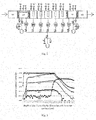
- FIG. 2 is a schematic structural view of the sputter equipment according to an embodiment of the present disclosure.
- the sputter equipment comprises: an input stage 100, an input chamber 200, a sputtering chamber 1, a sputtering chamber 2, a sputtering chamber 3, a sputtering chamber 4, a sputtering chamber 5, an unloading chamber 300 and an unloading stage 400.
- the sputter equipment also comprises a transmitting mechanism for transmitting the substrates one by one from the input stage 100 to input chamber 200, then to each sputtering chamber, and finally to the unloading chamber 300.
- the input chamber 200 is disposed prior to the sputtering chamber 1 for performing a temperature processing (for example, a heating) and a vacuum preprocessing for the substrate to be sputtered. Because there is not any target and/or other element in the input chamber 200, an internal volume of the input chamber 200 may be designed relatively smaller. In one embodiment, the internal volume of the input chamber 200 is less than or equal to an internal volume of each sputtering chamber. A vacuum of the sputtering chamber 1 is not destroyed when the substrate is transmitted from the input chamber 200 into the sputtering chamber 1.
- a purpose of disposing the input chamber 200 as a buffer chamber lies in that the input chamber 200 takes the place of the sputtering chamber to be exposed in an atmospheric environment, to prevent the target in the sputtering chamber from contacting steam, impurity and dust in the atmosphere, thus improving a process quality.
- the substrate is transmitted to the sputtering chamber 3, where a CuIn x Ga 1-x Se 2 (0.4 ⁇ x ⁇ 0.6) alloy target 3 is mounted, and a sputtering with a power density ranging from 2W/cm 2 to 3W/cm 2 is performed with the alloy target 3 for 1-2 minutes.
- the substrate is transmitted to the sputtering chamber 4, where a CuIn x Ga 1-x Se 2 (0.6 ⁇ x ⁇ 0.7) alloy target 4 is mounted, and a sputtering with a power density ranging from 2W/cm 2 to 3W/cm 2 is performed with the alloy target 4 for 1-2 minutes.
- a thickness of the Cu-In-Ga-Se absorbing layer disposed on the molybdenum back electrode ranges from 1.5 ⁇ m to 2 ⁇ m.
- a working pressure of each sputtering chamber is 1 ⁇ 10 -4 Torr, and a temperature of the substrate is maintained at any temperature between 200°C and 450°C. The sputtered substrate is transmitted to the unloading chamber.
- a purpose of the unloading chamber is similar with that of the input chamber 200, that is, a vacuum of the sputtering chamber 5 is not destroyed when the substrate is transmitted from the sputtering chamber 5 to the unloading chamber, and an annealing or other thermal processing may be performed in the unloading chamber 300.
- An internal volume of the unloading chamber 300 is less than or equal to the internal volume of each sputtering chamber. Then the substrate is transmitted to the unloading stage 400 to be collected in a substrate basket.
- the five sputtering chambers are explanatory and illustrative, which are used to generally understand the present disclosure. According to practice, those skilled in the art may use 2-4 sputtering chambers, even more then 5, such as 6, 7 or 8 sputtering chambers. It can be understood that, when the number of the sputtering chambers is different and/or the thickness of the Cu-In-Ga-Se absorbing layer is different, accordingly, x of the CuIn x Ga 1-x Se 2 alloy target will be different.
- the unloading chamber 300 is vacuumized, and an annealing is performed for the Cu-In-Ga-Se absorbing layer in a rapid heating mode in the unloading chamber 300 under a temperature of 400-600°C for 55-90 seconds. During the annealing process, it is not required to input any gas. During the annealing process, Ga ions diffuse from a high concentration part to a low concentration part so that the Ga concentration in the Cu-In-Ga-Se absorbing layer has agradient. The Ga concentration has a maximum on a surface of the Cu-In-Ga-Se absorbing layer contacting with the molybdenum back electrode, and has a minimum on the other surface of the Cu-In-Ga-Se absorbing layer.
- the Cu-In-Ga-Se absorbing layer After the annealing, the Cu-In-Ga-Se absorbing layer has a chalcopyrite structure, and a local ions diffusion occurs because of thermal energy, thus improving a crystalline state of the absorbing layer as well as the photovoltaic power generation efficiency of the primary absorbing layer of the solar cell.
- the annealing process will be explained in more details herein.
- the Ga concentration in the Cu-In-Ga-Se absorbing layer has a step gradient.
- the Ga concentration in the Cu-In-Ga-Se absorbing layer has a step gradient.
- an In 2 Se 3 or ZnS buffer layer is fabricated on the absorbing layer by a vacuum magnetron sputtering with an In 2 Se 3 alloy target or a ZnS alloy target under a working pressure of 1-5 ⁇ 10 -3 Torr in an Ar ambience, and a temperature of the substrate is maintained at a room temperature.
- a thickness of the In 2 Se 3 or ZnS buffer layer ranges from 80nm to 120nm.
- an intrinsic zinc oxide high impedance layer is fabricated on the buffer layer by a radio frequency vacuum magnetron sputtering with an intrinsic zinc oxide (ZnO) target under a working pressure of 1-5 ⁇ 10 -3 Torr with a working frequency of 400K-2MHz in an Ar ambience, and a temperature of the substrate is maintained at a room temperature.
- a thickness of the buffer layer ranges from 0.1 ⁇ m to 0.5 ⁇ m.
- an indium tin oxide (In 2 O 3 :SnO 2 ) film low impedance layer is fabricated on the intrinsic zinc oxide high impedance layer by a vacuum direct current magnetron sputtering with an indium tin oxide target, in which a mass ratio of In 2 O 3 to SnO 2 is 9:1, under a working pressure of 1-5 ⁇ 10 -3 Torr in an Ar ambience mixed with 2-5% O 2 , and a temperature of the substrate is maintained at a room temperature.
- a thickness of the intrinsic zinc oxide low impedance layer ranges from 0.3 ⁇ m to 0.8 ⁇ m.
- an aluminum electrode is fabricated on the indium tin oxide film low impedance layer by a sputtering with an aluminum target.
- the Cu-In-Ga-Se film solar cell having a Ga concentration with gradient distribution is formed.
- FIG. 3 is a secondary ion mass spectrum (SIMS) curve chart of the absorbing layer of the Cu-In-Ga-Se film solar cell fabricated according to the above method. It can be seen from Fig. 3 that the Ga concentration has a maximum on the surface of the Cu-In-Ga-Se absorbing layer contacting with the molybdenum back electrode and gradually decreases towards the other surface of the Cu-In-Ga-Se absorbing layer, which indicates that a bandgap of the absorbing layer has a gradient distribution.
- SIMS secondary ion mass spectrum
- the method according to embodiments of the present disclosure has following advantages. All processes of the method are dry processes without using any chemical solvent or solution.
- the absorbing layer with a stable crystalline state is fabricated by one-step without additional selenylation or sulfurization process, thus greatly shortening a production period, reducing production equipment, and preventing an environmental pollution as well as a potential danger during a production.
- the method has advantages of simple process, low energy consumption and low cost.
Landscapes
- Chemical & Material Sciences (AREA)
- Engineering & Computer Science (AREA)
- Chemical Kinetics & Catalysis (AREA)
- Materials Engineering (AREA)
- Mechanical Engineering (AREA)
- Metallurgy (AREA)
- Organic Chemistry (AREA)
- Physics & Mathematics (AREA)
- Thermal Sciences (AREA)
- Photovoltaic Devices (AREA)
- Physical Vapour Deposition (AREA)
- Manufacturing & Machinery (AREA)
Applications Claiming Priority (2)
| Application Number | Priority Date | Filing Date | Title |
|---|---|---|---|
| CN201210249760.7A CN102751388B (zh) | 2012-07-18 | 2012-07-18 | 一种铜铟镓硒薄膜太阳能电池的制备方法 |
| PCT/CN2013/074096 WO2014012383A1 (zh) | 2012-07-18 | 2013-04-11 | 一种铜铟镓硒薄膜太阳能电池的制备方法 |
Publications (3)
| Publication Number | Publication Date |
|---|---|
| EP2876696A1 true EP2876696A1 (de) | 2015-05-27 |
| EP2876696A4 EP2876696A4 (de) | 2015-12-30 |
| EP2876696B1 EP2876696B1 (de) | 2018-11-28 |
Family
ID=47031415
Family Applications (1)
| Application Number | Title | Priority Date | Filing Date |
|---|---|---|---|
| EP13820355.9A Active EP2876696B1 (de) | 2012-07-18 | 2013-04-11 | Verfahren zur herstellung einer solarzelle mit kupfer-indium-gallium-selenid-schicht |
Country Status (4)
| Country | Link |
|---|---|
| US (1) | US9105801B2 (de) |
| EP (1) | EP2876696B1 (de) |
| CN (1) | CN102751388B (de) |
| WO (1) | WO2014012383A1 (de) |
Families Citing this family (9)
| Publication number | Priority date | Publication date | Assignee | Title |
|---|---|---|---|---|
| US8586457B1 (en) * | 2012-05-17 | 2013-11-19 | Intermolecular, Inc. | Method of fabricating high efficiency CIGS solar cells |
| CN102694077B (zh) * | 2012-06-11 | 2014-08-06 | 林刘毓 | 一种铜铟镓硒薄膜太阳能电池的制备方法 |
| CN102751388B (zh) | 2012-07-18 | 2015-03-11 | 林刘毓 | 一种铜铟镓硒薄膜太阳能电池的制备方法 |
| CN103700725B (zh) * | 2013-12-27 | 2016-04-20 | 渤海大学 | 一种用于太阳能电池的基于纳米粒子铜铟硫硒薄膜的制备方法 |
| CN103695851B (zh) * | 2013-12-27 | 2016-02-24 | 柳州百韧特先进材料有限公司 | 溅射法制备柔性太阳能电池cigs吸收层和缓冲层的方法 |
| CN105097980B (zh) * | 2014-05-14 | 2018-08-03 | 香港中文大学 | 薄膜太阳能电池及其制造方法 |
| US9859450B2 (en) * | 2016-08-01 | 2018-01-02 | Solar-Tectic, Llc | CIGS/silicon thin-film tandem solar cell |
| CN108269862B (zh) * | 2017-12-11 | 2020-04-07 | 昆明理工大学 | 一种基于磁控溅射法的czts叠合吸收层及其制备方法 |
| CN113078242A (zh) * | 2021-04-29 | 2021-07-06 | 保定嘉盛光电科技股份有限公司 | 一种大面积铜铟镓硒电池组件生产装置及其方法 |
Family Cites Families (28)
| Publication number | Priority date | Publication date | Assignee | Title |
|---|---|---|---|---|
| JP3249408B2 (ja) * | 1996-10-25 | 2002-01-21 | 昭和シェル石油株式会社 | 薄膜太陽電池の薄膜光吸収層の製造方法及び製造装置 |
| AU2003275239A1 (en) * | 2002-09-30 | 2004-04-23 | Miasole | Manufacturing apparatus and method for large-scale production of thin-film solar cells |
| CN1865489A (zh) * | 2006-01-06 | 2006-11-22 | 浙江大学 | 贴片电感骨架的连续镀膜装置 |
| US20100059385A1 (en) * | 2008-09-06 | 2010-03-11 | Delin Li | Methods for fabricating thin film solar cells |
| US8894826B2 (en) * | 2009-09-24 | 2014-11-25 | Jesse A. Frantz | Copper indium gallium selenide (CIGS) thin films with composition controlled by co-sputtering |
| CN102054897B (zh) * | 2009-10-27 | 2012-03-28 | 成都先锋材料有限公司 | 多元素合金单一靶材制备薄膜太阳能电池的方法 |
| EP2497123A2 (de) * | 2009-11-05 | 2012-09-12 | Dow Global Technologies LLC | Herstellung von n-typ-chalkogenidzusammensetzungen und ihre verwendung für pv-module |
| JP4793504B2 (ja) * | 2009-11-06 | 2011-10-12 | 三菱マテリアル株式会社 | スパッタリングターゲット及びその製造方法 |
| WO2011083647A1 (ja) * | 2010-01-07 | 2011-07-14 | Jx日鉱日石金属株式会社 | Cu-Ga系スパッタリングターゲット、同ターゲットの製造方法、光吸収層及び該光吸収層を用いた太陽電池 |
| TWI514608B (zh) * | 2010-01-14 | 2015-12-21 | Dow Global Technologies Llc | 具曝露式導電柵格之防溼光伏打裝置 |
| US20110174363A1 (en) * | 2010-01-21 | 2011-07-21 | Aqt Solar, Inc. | Control of Composition Profiles in Annealed CIGS Absorbers |
| JP4831258B2 (ja) * | 2010-03-18 | 2011-12-07 | 三菱マテリアル株式会社 | スパッタリングターゲット及びその製造方法 |
| CN201648514U (zh) * | 2010-03-31 | 2010-11-24 | 甘国工 | 生产平板太阳能吸热镀膜板的立式镀膜装置 |
| US8546176B2 (en) * | 2010-04-22 | 2013-10-01 | Tsmc Solid State Lighting Ltd. | Forming chalcogenide semiconductor absorbers |
| US8927322B2 (en) * | 2010-05-04 | 2015-01-06 | Intermolecular, Inc. | Combinatorial methods for making CIGS solar cells |
| JP2011241452A (ja) * | 2010-05-19 | 2011-12-01 | Hitachi Cable Ltd | Cu−Ga合金材、スパッタリングターゲット、及びCu−Ga合金材の製造方法 |
| US8044477B1 (en) * | 2010-09-30 | 2011-10-25 | General Electric Company | Photovoltaic device and method for making |
| US7935558B1 (en) * | 2010-10-19 | 2011-05-03 | Miasole | Sodium salt containing CIG targets, methods of making and methods of use thereof |
| JP5725610B2 (ja) * | 2011-04-29 | 2015-05-27 | 三菱マテリアル株式会社 | スパッタリングターゲット及びその製造方法 |
| CN102354711B (zh) * | 2011-10-26 | 2013-09-04 | 香港中文大学 | 铜铟镓硒薄膜太阳能电池组件及其光吸收层的制备方法 |
| US20130164885A1 (en) * | 2011-12-21 | 2013-06-27 | Intermolecular, Inc. | Absorbers For High-Efficiency Thin-Film PV |
| CN102544132B (zh) * | 2012-01-17 | 2014-12-03 | 上海联孚新能源科技集团有限公司 | 铜铟镓硒电池及其制备方法 |
| US8586457B1 (en) * | 2012-05-17 | 2013-11-19 | Intermolecular, Inc. | Method of fabricating high efficiency CIGS solar cells |
| CN102694077B (zh) * | 2012-06-11 | 2014-08-06 | 林刘毓 | 一种铜铟镓硒薄膜太阳能电池的制备方法 |
| CN102751388B (zh) * | 2012-07-18 | 2015-03-11 | 林刘毓 | 一种铜铟镓硒薄膜太阳能电池的制备方法 |
| US20140113403A1 (en) * | 2012-08-27 | 2014-04-24 | Intermolecular Inc. | High efficiency CZTSe by a two-step approach |
| KR101382486B1 (ko) * | 2012-10-24 | 2014-04-08 | 한국과학기술연구원 | 페이스트 코팅법에 의해 제조된 양면 박막 태양전지 |
| JP2014209586A (ja) * | 2013-03-27 | 2014-11-06 | 株式会社リコー | 薄膜太陽電池及びその製造方法 |
-
2012
- 2012-07-18 CN CN201210249760.7A patent/CN102751388B/zh active Active
-
2013
- 2013-04-11 EP EP13820355.9A patent/EP2876696B1/de active Active
- 2013-04-11 WO PCT/CN2013/074096 patent/WO2014012383A1/zh not_active Ceased
-
2014
- 2014-01-11 US US14/153,028 patent/US9105801B2/en active Active
Also Published As
| Publication number | Publication date |
|---|---|
| EP2876696B1 (de) | 2018-11-28 |
| WO2014012383A1 (zh) | 2014-01-23 |
| CN102751388A (zh) | 2012-10-24 |
| US20140193943A1 (en) | 2014-07-10 |
| CN102751388B (zh) | 2015-03-11 |
| US9105801B2 (en) | 2015-08-11 |
| EP2876696A4 (de) | 2015-12-30 |
Similar Documents
| Publication | Publication Date | Title |
|---|---|---|
| EP2876696B1 (de) | Verfahren zur herstellung einer solarzelle mit kupfer-indium-gallium-selenid-schicht | |
| Bhattacharya et al. | 18.5% copper indium gallium diselenide (CIGS) device using single-layer, chemical-bath-deposited ZnS (O, OH) | |
| Powalla et al. | Highly efficient CIS solar cells and modules made by the co-evaporation process | |
| Kim et al. | Optimization of sputtered ZnS buffer for Cu2ZnSnS4 thin film solar cells | |
| Liu et al. | Preparation of Cu (In, Ga) Se2 thin film by sputtering from Cu (In, Ga) Se2 quaternary target | |
| CN102054897B (zh) | 多元素合金单一靶材制备薄膜太阳能电池的方法 | |
| JP6312996B2 (ja) | 光電変換素子および太陽電池 | |
| US20140053896A1 (en) | Method for producing the pentanary compound semiconductor cztsse, and thin-film solar cell | |
| US8969124B2 (en) | Method for fabricating Cu—In—Ga—Se film solar cell | |
| KR102594725B1 (ko) | 흡수체층의 후처리 방법 | |
| WO2011040645A1 (en) | Photoelectric conversion device, method for producing the same, and solar battery | |
| KR20120080045A (ko) | 태양전지의 제조방법 | |
| US20130327398A1 (en) | Thin-Film Photovoltaic Devices and Methods of Manufacture | |
| KR20150048728A (ko) | 화합물 태양 전지 및 그 제조 방법 | |
| WO2014025176A1 (ko) | Na 공급 방법이 개선된 유연기판 CIGS 태양전지 및 그 제조방법 | |
| KR101415251B1 (ko) | 다중 버퍼층 및 이를 포함하는 태양전지 및 그 생산방법 | |
| KR20140066964A (ko) | 태양전지 및 이의 제조방법 | |
| KR101734362B1 (ko) | Acigs 박막의 저온 형성방법과 이를 이용한 태양전지의 제조방법 | |
| CN114203842A (zh) | 宽禁带铜镓硒光吸收层及其制备方法、太阳能电池 | |
| KR101761565B1 (ko) | 태양 전지 및 이의 제조 방법 | |
| KR102212042B1 (ko) | 원자층 증착법으로 형성된 버퍼층을 포함하는 태양전지 및 이의 제조방법 | |
| KR101358055B1 (ko) | 태양전지용 CZTSe계 박막의 제조방법 및 그 방법에 의해 제조된 CZTSe계 박막 | |
| US20180240918A1 (en) | Photovoltaic devices including a chalcogenide-containing photovoltaic light-absorber, and related methods of making | |
| KR102025091B1 (ko) | CZT(S,Se)계 박막, 시드가 형성된 전구체층을 이용하는 CZT(S,Se)계 박막 형성방법 및 CZT(S,Se)계 박막 태양전지와 그 제조방법 | |
| EP2999004A1 (de) | Photoelektrische umwandlungsvorrichtung und solarzelle |
Legal Events
| Date | Code | Title | Description |
|---|---|---|---|
| PUAI | Public reference made under article 153(3) epc to a published international application that has entered the european phase |
Free format text: ORIGINAL CODE: 0009012 |
|
| 17P | Request for examination filed |
Effective date: 20150213 |
|
| AK | Designated contracting states |
Kind code of ref document: A1 Designated state(s): AL AT BE BG CH CY CZ DE DK EE ES FI FR GB GR HR HU IE IS IT LI LT LU LV MC MK MT NL NO PL PT RO RS SE SI SK SM TR |
|
| AX | Request for extension of the european patent |
Extension state: BA ME |
|
| DAX | Request for extension of the european patent (deleted) | ||
| RA4 | Supplementary search report drawn up and despatched (corrected) |
Effective date: 20151202 |
|
| RIC1 | Information provided on ipc code assigned before grant |
Ipc: H01L 31/18 20060101AFI20151126BHEP Ipc: C23C 14/06 20060101ALI20151126BHEP Ipc: C23C 14/34 20060101ALI20151126BHEP Ipc: H01L 21/02 20060101ALI20151126BHEP |
|
| REG | Reference to a national code |
Ref country code: DE Ref legal event code: R079 Ref document number: 602013047549 Country of ref document: DE Free format text: PREVIOUS MAIN CLASS: H01L0031180000 Ipc: C23C0014060000 |
|
| GRAP | Despatch of communication of intention to grant a patent |
Free format text: ORIGINAL CODE: EPIDOSNIGR1 |
|
| STAA | Information on the status of an ep patent application or granted ep patent |
Free format text: STATUS: GRANT OF PATENT IS INTENDED |
|
| RIC1 | Information provided on ipc code assigned before grant |
Ipc: C23C 14/34 20060101ALI20180530BHEP Ipc: C23C 14/06 20060101AFI20180530BHEP Ipc: C23C 14/58 20060101ALI20180530BHEP Ipc: H01L 31/18 20060101ALI20180530BHEP Ipc: C23C 14/56 20060101ALI20180530BHEP Ipc: H01L 21/02 20060101ALI20180530BHEP |
|
| INTG | Intention to grant announced |
Effective date: 20180615 |
|
| GRAS | Grant fee paid |
Free format text: ORIGINAL CODE: EPIDOSNIGR3 |
|
| GRAA | (expected) grant |
Free format text: ORIGINAL CODE: 0009210 |
|
| STAA | Information on the status of an ep patent application or granted ep patent |
Free format text: STATUS: THE PATENT HAS BEEN GRANTED |
|
| AK | Designated contracting states |
Kind code of ref document: B1 Designated state(s): AL AT BE BG CH CY CZ DE DK EE ES FI FR GB GR HR HU IE IS IT LI LT LU LV MC MK MT NL NO PL PT RO RS SE SI SK SM TR |
|
| RAP1 | Party data changed (applicant data changed or rights of an application transferred) |
Owner name: ZHANG, ZHUN Owner name: LIN, LIUYU |
|
| RIN1 | Information on inventor provided before grant (corrected) |
Inventor name: LIN, LIUYU Inventor name: ZHANG, ZHUN |
|
| REG | Reference to a national code |
Ref country code: CH Ref legal event code: EP |
|
| REG | Reference to a national code |
Ref country code: AT Ref legal event code: REF Ref document number: 1070318 Country of ref document: AT Kind code of ref document: T Effective date: 20181215 |
|
| REG | Reference to a national code |
Ref country code: IE Ref legal event code: FG4D |
|
| REG | Reference to a national code |
Ref country code: DE Ref legal event code: R096 Ref document number: 602013047549 Country of ref document: DE |
|
| REG | Reference to a national code |
Ref country code: SE Ref legal event code: TRGR |
|
| REG | Reference to a national code |
Ref country code: NL Ref legal event code: MP Effective date: 20181128 |
|
| REG | Reference to a national code |
Ref country code: LT Ref legal event code: MG4D |
|
| REG | Reference to a national code |
Ref country code: AT Ref legal event code: MK05 Ref document number: 1070318 Country of ref document: AT Kind code of ref document: T Effective date: 20181128 |
|
| PG25 | Lapsed in a contracting state [announced via postgrant information from national office to epo] |
Ref country code: FI Free format text: LAPSE BECAUSE OF FAILURE TO SUBMIT A TRANSLATION OF THE DESCRIPTION OR TO PAY THE FEE WITHIN THE PRESCRIBED TIME-LIMIT Effective date: 20181128 Ref country code: NO Free format text: LAPSE BECAUSE OF FAILURE TO SUBMIT A TRANSLATION OF THE DESCRIPTION OR TO PAY THE FEE WITHIN THE PRESCRIBED TIME-LIMIT Effective date: 20190228 Ref country code: LV Free format text: LAPSE BECAUSE OF FAILURE TO SUBMIT A TRANSLATION OF THE DESCRIPTION OR TO PAY THE FEE WITHIN THE PRESCRIBED TIME-LIMIT Effective date: 20181128 Ref country code: AT Free format text: LAPSE BECAUSE OF FAILURE TO SUBMIT A TRANSLATION OF THE DESCRIPTION OR TO PAY THE FEE WITHIN THE PRESCRIBED TIME-LIMIT Effective date: 20181128 Ref country code: HR Free format text: LAPSE BECAUSE OF FAILURE TO SUBMIT A TRANSLATION OF THE DESCRIPTION OR TO PAY THE FEE WITHIN THE PRESCRIBED TIME-LIMIT Effective date: 20181128 Ref country code: ES Free format text: LAPSE BECAUSE OF FAILURE TO SUBMIT A TRANSLATION OF THE DESCRIPTION OR TO PAY THE FEE WITHIN THE PRESCRIBED TIME-LIMIT Effective date: 20181128 Ref country code: IS Free format text: LAPSE BECAUSE OF FAILURE TO SUBMIT A TRANSLATION OF THE DESCRIPTION OR TO PAY THE FEE WITHIN THE PRESCRIBED TIME-LIMIT Effective date: 20190328 Ref country code: BG Free format text: LAPSE BECAUSE OF FAILURE TO SUBMIT A TRANSLATION OF THE DESCRIPTION OR TO PAY THE FEE WITHIN THE PRESCRIBED TIME-LIMIT Effective date: 20190228 Ref country code: LT Free format text: LAPSE BECAUSE OF FAILURE TO SUBMIT A TRANSLATION OF THE DESCRIPTION OR TO PAY THE FEE WITHIN THE PRESCRIBED TIME-LIMIT Effective date: 20181128 |
|
| PG25 | Lapsed in a contracting state [announced via postgrant information from national office to epo] |
Ref country code: AL Free format text: LAPSE BECAUSE OF FAILURE TO SUBMIT A TRANSLATION OF THE DESCRIPTION OR TO PAY THE FEE WITHIN THE PRESCRIBED TIME-LIMIT Effective date: 20181128 Ref country code: PT Free format text: LAPSE BECAUSE OF FAILURE TO SUBMIT A TRANSLATION OF THE DESCRIPTION OR TO PAY THE FEE WITHIN THE PRESCRIBED TIME-LIMIT Effective date: 20190328 Ref country code: GR Free format text: LAPSE BECAUSE OF FAILURE TO SUBMIT A TRANSLATION OF THE DESCRIPTION OR TO PAY THE FEE WITHIN THE PRESCRIBED TIME-LIMIT Effective date: 20190301 Ref country code: RS Free format text: LAPSE BECAUSE OF FAILURE TO SUBMIT A TRANSLATION OF THE DESCRIPTION OR TO PAY THE FEE WITHIN THE PRESCRIBED TIME-LIMIT Effective date: 20181128 |
|
| PG25 | Lapsed in a contracting state [announced via postgrant information from national office to epo] |
Ref country code: NL Free format text: LAPSE BECAUSE OF FAILURE TO SUBMIT A TRANSLATION OF THE DESCRIPTION OR TO PAY THE FEE WITHIN THE PRESCRIBED TIME-LIMIT Effective date: 20181128 |
|
| PG25 | Lapsed in a contracting state [announced via postgrant information from national office to epo] |
Ref country code: CZ Free format text: LAPSE BECAUSE OF FAILURE TO SUBMIT A TRANSLATION OF THE DESCRIPTION OR TO PAY THE FEE WITHIN THE PRESCRIBED TIME-LIMIT Effective date: 20181128 Ref country code: PL Free format text: LAPSE BECAUSE OF FAILURE TO SUBMIT A TRANSLATION OF THE DESCRIPTION OR TO PAY THE FEE WITHIN THE PRESCRIBED TIME-LIMIT Effective date: 20181128 Ref country code: DK Free format text: LAPSE BECAUSE OF FAILURE TO SUBMIT A TRANSLATION OF THE DESCRIPTION OR TO PAY THE FEE WITHIN THE PRESCRIBED TIME-LIMIT Effective date: 20181128 |
|
| REG | Reference to a national code |
Ref country code: DE Ref legal event code: R097 Ref document number: 602013047549 Country of ref document: DE |
|
| PG25 | Lapsed in a contracting state [announced via postgrant information from national office to epo] |
Ref country code: SM Free format text: LAPSE BECAUSE OF FAILURE TO SUBMIT A TRANSLATION OF THE DESCRIPTION OR TO PAY THE FEE WITHIN THE PRESCRIBED TIME-LIMIT Effective date: 20181128 Ref country code: EE Free format text: LAPSE BECAUSE OF FAILURE TO SUBMIT A TRANSLATION OF THE DESCRIPTION OR TO PAY THE FEE WITHIN THE PRESCRIBED TIME-LIMIT Effective date: 20181128 Ref country code: SK Free format text: LAPSE BECAUSE OF FAILURE TO SUBMIT A TRANSLATION OF THE DESCRIPTION OR TO PAY THE FEE WITHIN THE PRESCRIBED TIME-LIMIT Effective date: 20181128 Ref country code: RO Free format text: LAPSE BECAUSE OF FAILURE TO SUBMIT A TRANSLATION OF THE DESCRIPTION OR TO PAY THE FEE WITHIN THE PRESCRIBED TIME-LIMIT Effective date: 20181128 |
|
| PLBE | No opposition filed within time limit |
Free format text: ORIGINAL CODE: 0009261 |
|
| STAA | Information on the status of an ep patent application or granted ep patent |
Free format text: STATUS: NO OPPOSITION FILED WITHIN TIME LIMIT |
|
| PG25 | Lapsed in a contracting state [announced via postgrant information from national office to epo] |
Ref country code: SI Free format text: LAPSE BECAUSE OF FAILURE TO SUBMIT A TRANSLATION OF THE DESCRIPTION OR TO PAY THE FEE WITHIN THE PRESCRIBED TIME-LIMIT Effective date: 20181128 |
|
| 26N | No opposition filed |
Effective date: 20190829 |
|
| REG | Reference to a national code |
Ref country code: CH Ref legal event code: PL |
|
| REG | Reference to a national code |
Ref country code: BE Ref legal event code: MM Effective date: 20190430 |
|
| PG25 | Lapsed in a contracting state [announced via postgrant information from national office to epo] |
Ref country code: MC Free format text: LAPSE BECAUSE OF FAILURE TO SUBMIT A TRANSLATION OF THE DESCRIPTION OR TO PAY THE FEE WITHIN THE PRESCRIBED TIME-LIMIT Effective date: 20181128 Ref country code: LU Free format text: LAPSE BECAUSE OF NON-PAYMENT OF DUE FEES Effective date: 20190411 |
|
| PG25 | Lapsed in a contracting state [announced via postgrant information from national office to epo] |
Ref country code: CH Free format text: LAPSE BECAUSE OF NON-PAYMENT OF DUE FEES Effective date: 20190430 Ref country code: LI Free format text: LAPSE BECAUSE OF NON-PAYMENT OF DUE FEES Effective date: 20190430 |
|
| PG25 | Lapsed in a contracting state [announced via postgrant information from national office to epo] |
Ref country code: BE Free format text: LAPSE BECAUSE OF NON-PAYMENT OF DUE FEES Effective date: 20190430 |
|
| PG25 | Lapsed in a contracting state [announced via postgrant information from national office to epo] |
Ref country code: TR Free format text: LAPSE BECAUSE OF FAILURE TO SUBMIT A TRANSLATION OF THE DESCRIPTION OR TO PAY THE FEE WITHIN THE PRESCRIBED TIME-LIMIT Effective date: 20181128 |
|
| PG25 | Lapsed in a contracting state [announced via postgrant information from national office to epo] |
Ref country code: IE Free format text: LAPSE BECAUSE OF NON-PAYMENT OF DUE FEES Effective date: 20190411 |
|
| PG25 | Lapsed in a contracting state [announced via postgrant information from national office to epo] |
Ref country code: CY Free format text: LAPSE BECAUSE OF FAILURE TO SUBMIT A TRANSLATION OF THE DESCRIPTION OR TO PAY THE FEE WITHIN THE PRESCRIBED TIME-LIMIT Effective date: 20181128 |
|
| PG25 | Lapsed in a contracting state [announced via postgrant information from national office to epo] |
Ref country code: HU Free format text: LAPSE BECAUSE OF FAILURE TO SUBMIT A TRANSLATION OF THE DESCRIPTION OR TO PAY THE FEE WITHIN THE PRESCRIBED TIME-LIMIT; INVALID AB INITIO Effective date: 20130411 Ref country code: MT Free format text: LAPSE BECAUSE OF FAILURE TO SUBMIT A TRANSLATION OF THE DESCRIPTION OR TO PAY THE FEE WITHIN THE PRESCRIBED TIME-LIMIT Effective date: 20181128 |
|
| PG25 | Lapsed in a contracting state [announced via postgrant information from national office to epo] |
Ref country code: MK Free format text: LAPSE BECAUSE OF FAILURE TO SUBMIT A TRANSLATION OF THE DESCRIPTION OR TO PAY THE FEE WITHIN THE PRESCRIBED TIME-LIMIT Effective date: 20181128 |
|
| PGFP | Annual fee paid to national office [announced via postgrant information from national office to epo] |
Ref country code: DE Payment date: 20250417 Year of fee payment: 13 |
|
| PGFP | Annual fee paid to national office [announced via postgrant information from national office to epo] |
Ref country code: IT Payment date: 20250430 Year of fee payment: 13 |
|
| PGFP | Annual fee paid to national office [announced via postgrant information from national office to epo] |
Ref country code: FR Payment date: 20250417 Year of fee payment: 13 |
|
| PGFP | Annual fee paid to national office [announced via postgrant information from national office to epo] |
Ref country code: SE Payment date: 20250423 Year of fee payment: 13 |
|
| PGFP | Annual fee paid to national office [announced via postgrant information from national office to epo] |
Ref country code: GB Payment date: 20260325 Year of fee payment: 14 |