EP2876979A1 - Carte de circuits imprimés avec inserts en céramique - Google Patents
Carte de circuits imprimés avec inserts en céramique Download PDFInfo
- Publication number
- EP2876979A1 EP2876979A1 EP14003954.6A EP14003954A EP2876979A1 EP 2876979 A1 EP2876979 A1 EP 2876979A1 EP 14003954 A EP14003954 A EP 14003954A EP 2876979 A1 EP2876979 A1 EP 2876979A1
- Authority
- EP
- European Patent Office
- Prior art keywords
- circuit board
- printed circuit
- thermally conductive
- conductive element
- electrical component
- Prior art date
- Legal status (The legal status is an assumption and is not a legal conclusion. Google has not performed a legal analysis and makes no representation as to the accuracy of the status listed.)
- Granted
Links
Images
Classifications
-
- H—ELECTRICITY
- H05—ELECTRIC TECHNIQUES NOT OTHERWISE PROVIDED FOR
- H05K—PRINTED CIRCUITS; CASINGS OR CONSTRUCTIONAL DETAILS OF ELECTRIC APPARATUS; MANUFACTURE OF ASSEMBLAGES OF ELECTRICAL COMPONENTS
- H05K1/00—Printed circuits
- H05K1/02—Details
- H05K1/0201—Thermal arrangements, e.g. for cooling, heating or preventing overheating
- H05K1/0203—Cooling of mounted components
- H05K1/0204—Cooling of mounted components using means for thermal conduction connection in the thickness direction of the substrate
-
- H—ELECTRICITY
- H05—ELECTRIC TECHNIQUES NOT OTHERWISE PROVIDED FOR
- H05K—PRINTED CIRCUITS; CASINGS OR CONSTRUCTIONAL DETAILS OF ELECTRIC APPARATUS; MANUFACTURE OF ASSEMBLAGES OF ELECTRICAL COMPONENTS
- H05K1/00—Printed circuits
- H05K1/02—Details
- H05K1/0201—Thermal arrangements, e.g. for cooling, heating or preventing overheating
- H05K1/0203—Cooling of mounted components
- H05K1/0207—Cooling of mounted components using internal conductor planes parallel to the surface for thermal conduction, e.g. power planes
-
- H—ELECTRICITY
- H05—ELECTRIC TECHNIQUES NOT OTHERWISE PROVIDED FOR
- H05K—PRINTED CIRCUITS; CASINGS OR CONSTRUCTIONAL DETAILS OF ELECTRIC APPARATUS; MANUFACTURE OF ASSEMBLAGES OF ELECTRICAL COMPONENTS
- H05K1/00—Printed circuits
- H05K1/02—Details
- H05K1/0296—Conductive pattern lay-out details not covered by sub groups H05K1/02 - H05K1/0295
- H05K1/0298—Multilayer circuits
-
- H—ELECTRICITY
- H05—ELECTRIC TECHNIQUES NOT OTHERWISE PROVIDED FOR
- H05K—PRINTED CIRCUITS; CASINGS OR CONSTRUCTIONAL DETAILS OF ELECTRIC APPARATUS; MANUFACTURE OF ASSEMBLAGES OF ELECTRICAL COMPONENTS
- H05K1/00—Printed circuits
- H05K1/02—Details
- H05K1/11—Printed elements for providing electric connections to or between printed circuits
- H05K1/115—Via connections; Lands around holes or via connections
-
- H—ELECTRICITY
- H05—ELECTRIC TECHNIQUES NOT OTHERWISE PROVIDED FOR
- H05K—PRINTED CIRCUITS; CASINGS OR CONSTRUCTIONAL DETAILS OF ELECTRIC APPARATUS; MANUFACTURE OF ASSEMBLAGES OF ELECTRICAL COMPONENTS
- H05K1/00—Printed circuits
- H05K1/18—Printed circuits structurally associated with non-printed electric components
- H05K1/181—Printed circuits structurally associated with non-printed electric components associated with surface mounted components
-
- H—ELECTRICITY
- H05—ELECTRIC TECHNIQUES NOT OTHERWISE PROVIDED FOR
- H05K—PRINTED CIRCUITS; CASINGS OR CONSTRUCTIONAL DETAILS OF ELECTRIC APPARATUS; MANUFACTURE OF ASSEMBLAGES OF ELECTRICAL COMPONENTS
- H05K2201/00—Indexing scheme relating to printed circuits covered by H05K1/00
- H05K2201/10—Details of components or other objects attached to or integrated in a printed circuit board
- H05K2201/10227—Other objects, e.g. metallic pieces
- H05K2201/10416—Metallic blocks or heatsinks completely inserted in a PCB
-
- H—ELECTRICITY
- H10—SEMICONDUCTOR DEVICES; ELECTRIC SOLID-STATE DEVICES NOT OTHERWISE PROVIDED FOR
- H10W—GENERIC PACKAGES, INTERCONNECTIONS, CONNECTORS OR OTHER CONSTRUCTIONAL DETAILS OF DEVICES COVERED BY CLASS H10
- H10W90/00—Package configurations
- H10W90/701—Package configurations characterised by the relative positions of pads or connectors relative to package parts
- H10W90/721—Package configurations characterised by the relative positions of pads or connectors relative to package parts of bump connectors
- H10W90/724—Package configurations characterised by the relative positions of pads or connectors relative to package parts of bump connectors between a chip and a stacked insulating package substrate, interposer or RDL
Definitions
- the invention relates to a printed circuit board, in particular a multilayer electrical circuit board for receiving electrical components, and an electrical component with such a printed circuit board.
- printed circuit boards are equipped with electrical or electronic components.
- the printed circuit boards are used for the mechanical fixing and the electrical coupling of components arranged on a printed circuit board.
- the electrical connections are made by means of conductor tracks, for example copper conductor tracks.
- a printed circuit board can be constructed in multiple layers and have a plurality of printed circuit layers or layers. This makes it possible that each conductor track or layer is provided individually with electrically conductive tracks, whereby the number of possible electrical connections between the arranged on the circuit board components can be increased.
- a conductor track or layer may have a recess or an opening, which makes it possible to produce an electrical connection between tracks on different tracks, for example by coating the opening or the break with electrically conductive material or an electrically conductive material in the recess or the breakthrough is arranged and electrically connected to the interconnects to be connected.
- EP 0 926 929 A1 describes a multi-layer printed circuit board with a plurality of superposed by Isolierstofflagen separated interconnect levels. Disposed between the outer insulating layers is a core substrate which adjusts the thermal expansion characteristics of the multilayer printed circuit board to thermal expansion characteristics of a device disposed on the multilayer printed circuit board.
- the core substrate is made of molybdenum.
- a printed circuit board which is designed to be equipped with electrical components.
- the printed circuit board has a plurality of conductor track planes arranged one above the other, with two adjacent track track planes being insulated from one another by an insulation layer.
- the printed circuit board is characterized in that between a first outer insulating layer and a second outer insulating layer, a thermally conductive element is arranged, wherein the thermally conductive element comprises ceramic.
- the basic geometric structure of the printed circuit board corresponds to a so-called sandwich structure, wherein in a depth direction of the printed circuit board electrically conductive layers, the printed circuit layers, alternate with electrically insulating layers, the insulation layers.
- a core is arranged, which is thermally conductive and consists of ceramic.
- the electrical components can be arranged on the first outer surface.
- the thermally conductive element by its properties and by its arrangement within the printed circuit board, enables heat conduction, in particular heat dissipation, from the first outer surface and the electrical components to the second outer surface, which is, for example, opposite or also transverse to the first outer surface ,
- Ceramic is suitable for use as a thermally conductive element, since in addition to good thermal conductivity as a rule, also a good voltage insulation, in particular a high voltage insulation allows and has advantageous mechanical properties in terms of its rigidity.
- a printed circuit board as described above and below, in particular for uses in high voltage systems and in vacuum may be advantageous.
- Such a scenario is given for example in the field of use of satellites, which are located in a vacuum.
- Thermal energy can be derived as a heat flux in a solid due to a temperature difference (heat diffusion or conduction) or by a macroscopic material flow (convection) from a heat source towards a heat sink.
- a heat transfer can also be effected by thermal radiation.
- Thermal energy can not be transferred by convection in a vacuum or almost empty room, because, for example, there is no air flow to transport the heat energy. This can help with the use of technical and / or electrical devices in a vacuum, a possibly required cooling of electrical components by convection does not occur.
- a heat conduction in a vacuum is thus limited to conduction and heat radiation.
- ceramic is a good thermal conductor and thus offers the possibility of transporting thermal energy through conduction.
- ceramics also meet requirements with regard to high-voltage insulation, so that the printed circuit board as described above and below is particularly suitable for use in a power amplifier in satellites.
- the ceramic of the thermally conductive element may in particular have a higher thermal conductivity than the material of the insulating layers of the printed circuit board.
- the thermally conductive element comprises aluminum nitride.
- Aluminum nitrite is characterized by a particularly good thermal conductivity.
- the thermally conductive element is designed to be electrically insulating.
- good thermal conductors are also electrically conductive.
- this material thus represents an advantageous combination of good thermal conductivity and electrical insulation.
- the thermally conductive element is arranged in a recess of an insulating layer.
- the printed circuit board can be constructed in multiple layers, wherein the insulation layers are thicker in the depth direction than the conductor tracks. If a recess or even a breakthrough is provided in one of the inner insulation layers, the thermally conductive element can be arranged as the core of the printed circuit board without the printed circuit board having its outward visible geometric dimensions changes. Furthermore, the thermally conductive element is fixed by the recess in its position.
- the recess may be a depression in an insulating layer or a breakthrough by an insulating layer.
- the recess may also extend over more than one insulation layer in the depth direction of the printed circuit board.
- a first surface of the thermally conductive element in the depth direction (104) of the printed circuit board is adjacent to a first interconnect level.
- the first interconnect level is usually provided with an electrically conductive material, this also has a high thermal conductivity. Thus, the thermal energy can be conducted from the first surface of the circuit board via the interconnects of the interconnect level to the thermally conductive element and transported by the latter.
- conductor tracks of the conductor track plane run on or along the first surface of the thermally conductive element.
- a second surface of the thermally conductive element in the depth direction of the printed circuit board is adjacent to a second printed circuit board plane.
- thermal energy can be dissipated from the thermal paths by interconnects of a first interconnect level to the thermally conductive element and by interconnects of a second interconnect level be guided conductive element.
- the thermally conductive element extends in the depth direction of the printed circuit board over more than one insulating layer.
- an electrical component for use in a satellite has a printed circuit board as described above and below and an electrical component which is mechanically and electrically coupled to a mounting position of the printed circuit board.
- the thermally conductive element is arranged so that it overlaps the electrical component in the longitudinal direction of the printed circuit board.
- the electrical component may, for example, be a power amplifier for a satellite, for example a power amplifier in the form of a traveling-wave tube amplifier.
- a power amplifier in the form of a traveling-wave tube amplifier.
- One such consists of a traveling wave tube which primarily determines the RF characteristics and a power supply which generates the supply voltages, primarily high voltages, and constitutes a telemetry and telecommand interface to the satellite.
- rectifier stages connected in series can be used. These include lossy rectifier diodes, which in turn are high-voltage insulated by the series circuit with respect to a heat sink, such as a housing. Due to the absence of air or other ambient gas and thus the lack of the possibility of convection cooling space for equipment the resulting power loss of the electrical components, ie the excess thermal energy to be dissipated via the circuit board, ie by conduction, and heat radiation.
- Overlapping means that a vertical projection of the electrical component on a surface of the circuit board (as a projection surface, or limited to the longitudinal direction referred to as longitudinal projection) a Has overlap region with a vertical projection of the thermally conductive element on the same surface of the circuit board.
- the thermally conductive element may at least partially, completely, or exactly overlap the electrically conductive component.
- a complete overlap means that the thermally conductive element has a longitudinal projection which is larger than the longitudinal projection of the electrical component.
- An exact overlap means that these two longitudinal projections are identical and overlap without overlap, ie are congruent.
- the longitudinal projections may be identical or different and are offset from each other.
- the thermally conductive element is arranged such that it overlaps the electrical component in the transverse direction of the printed circuit board.
- the electrical component has a thermal coupling element, which is thermally coupled to an outer layer of the printed circuit board and designed to dissipate heat from the printed circuit board, wherein the thermally conductive element is arranged so that it is the thermal coupling element in the longitudinal direction of the printed circuit board overlaps.
- the outer layer is arranged opposite the assembly position. This results in a thermal flow of the electrical component on the Be Publishedungslage, the thermally conductive elements, the outer layer and the thermal coupling element.
- the thermal coupling element is designed, for example, to be electrically, mechanically and thermally coupled to a housing of the electrical component.
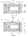
- Fig. 1 shows a layered printed circuit board 100 having a plurality of conductor tracks 180, which is designed as an electrically conductive layer, for example made of copper or copper foils.
- An insulating layer 190A, 190B, 190C, 190D is arranged in each case between two conductor track planes 180 adjacent in the depth direction of the printed circuit board.
- the electrical connection between adjacent interconnect levels may be made, for example, by a ply connection 170 extending in the depth direction of the circuit board 100 between interconnect levels.
- An electrical component 200 is coupled to the mounting layer 110.
- An inner layer 120 has a layer spacing 150 to the mounting position.
- the layer spacing 150 corresponds to the thickness of an insulation layer 190A.
- the electrical component 200 has a laterally extending isolation distance 160 to a fastening sleeve 140 of the printed circuit board.
- An outer layer 130 is arranged on a surface of the printed circuit board 100 arranged opposite to the mounting position 110.
- the printed circuit board 100 has six insulation layers. In the two insulation layers arranged centrally in the depth direction, a recess is arranged in which the thermally conductive element 300 is located.
- the thermally conductive element 300 extends in the depth direction of the printed circuit board 100 via two insulating layers.
- Fig. 2 shows the heat flow in a printed circuit board 100 from the electrical component 200 via the printed circuit board 100 and the thermally conductive element 300 to a thermal coupling element 210.
- the longitudinal direction 102 of the circuit board 100 extends in the plane of the Fig. 2 left to right.
- a projection of the thermally conductive element 300 onto the mounting position overlaps in the longitudinal direction a projection of the electrical component 200 onto the mounting position. The same applies to the projections of the thermally conductive element 300 and the thermal coupling element 210 on the outer layer 130th
- the depth direction 104 of the circuit board 100 extends in the plane of the Fig. 2 from top to bottom.
- the heat flow 205A, 205B is indicated by arrows.
- the transverse direction of the circuit board is perpendicular to the depth direction and to the longitudinal direction, ie in the plane of the Fig. 2 into it.
- a first surface 302 and a second surface 304 of the thermally conductive element 300 each adjoin a conductor track plane between two adjacent insulation layers.
- the heat flow 205A, 205B can be described as follows:
- the heat emitted by the power loss of a lossy, high-voltage-operated component 200 can be introduced into the ceramic core 300 via the mounting layer 110 and inner layer 120 and via the insulation layers.
- the ceramic core conducts the heat to the next expanding copper foil, i. to the second surface 304, and to the thermal coupling element 210, without exceeding a predetermined high voltage load or Feldstardauerbestelastung.
- a voltage flashover between the device 200 and the mechanical / thermal connection 140 can be prevented.
Landscapes
- Engineering & Computer Science (AREA)
- Microelectronics & Electronic Packaging (AREA)
- Production Of Multi-Layered Print Wiring Board (AREA)
- Structure Of Printed Boards (AREA)
- Cooling Or The Like Of Semiconductors Or Solid State Devices (AREA)
Applications Claiming Priority (1)
| Application Number | Priority Date | Filing Date | Title |
|---|---|---|---|
| DE102013019617.5A DE102013019617B4 (de) | 2013-11-25 | 2013-11-25 | Elektrische Hochspannungskomponente zur Verwendung in einem Satelliten sowie Satellit damit |
Publications (2)
| Publication Number | Publication Date |
|---|---|
| EP2876979A1 true EP2876979A1 (fr) | 2015-05-27 |
| EP2876979B1 EP2876979B1 (fr) | 2019-08-14 |
Family
ID=51999201
Family Applications (1)
| Application Number | Title | Priority Date | Filing Date |
|---|---|---|---|
| EP14003954.6A Active EP2876979B1 (fr) | 2013-11-25 | 2014-11-24 | Carte de circuits imprimés avec inserts en céramique |
Country Status (5)
| Country | Link |
|---|---|
| US (1) | US10292254B2 (fr) |
| EP (1) | EP2876979B1 (fr) |
| JP (1) | JP2015103809A (fr) |
| CN (1) | CN104661425A (fr) |
| DE (1) | DE102013019617B4 (fr) |
Families Citing this family (10)
| Publication number | Priority date | Publication date | Assignee | Title |
|---|---|---|---|---|
| DE102014008148B4 (de) * | 2014-05-23 | 2020-06-04 | Continental Automotive Gmbh | Verfahren zur Herstellung einer Leiterplatte und Leiterplatte |
| DE102015226712B4 (de) * | 2014-12-26 | 2024-10-24 | Omron Corporation | Leiterplatte und elektronisches bauelement |
| JP6333215B2 (ja) * | 2015-05-19 | 2018-05-30 | オムロンオートモーティブエレクトロニクス株式会社 | プリント基板、電子装置 |
| EP3520584B1 (fr) | 2016-09-27 | 2026-01-14 | AT & S Austria Technologie & Systemtechnik Aktiengesellschaft | Structure ignifuge destinée à un support de composant |
| WO2019102601A1 (fr) * | 2017-11-27 | 2019-05-31 | 三菱電機株式会社 | Dispositif à semi-conducteur |
| JP7384121B2 (ja) * | 2020-07-09 | 2023-11-21 | Tdk株式会社 | 回路基板及びこれを用いた回路モジュール |
| WO2022085715A1 (fr) * | 2020-10-22 | 2022-04-28 | 株式会社村田製作所 | Structure multicouche et son procédé de fabrication |
| DE102020128729B4 (de) | 2020-11-02 | 2025-09-18 | Audi Aktiengesellschaft | Anordnung zum Austauschen von Wärme |
| CN116321670A (zh) * | 2021-12-03 | 2023-06-23 | 欣兴电子股份有限公司 | 电路板及其制造方法 |
| WO2024247133A1 (fr) * | 2023-05-30 | 2024-12-05 | 株式会社ダイワ工業 | Stratifié de carte de câblage et procédé de fabrication de stratifié de carte de câblage |
Citations (7)
| Publication number | Priority date | Publication date | Assignee | Title |
|---|---|---|---|---|
| EP0926929A1 (fr) | 1997-12-19 | 1999-06-30 | Robert Bosch Gmbh | Plaque à circuit imprimé multicouche |
| EP1261028A2 (fr) * | 2001-05-22 | 2002-11-27 | Hitachi, Ltd. | Arrangement de dissipation de chaleur pour dispositif électronique |
| EP1276357A2 (fr) * | 2001-07-13 | 2003-01-15 | Behr-Hella Thermocontrol GmbH | Panneau à conducteurs pour circuits électriques |
| US20070284711A1 (en) * | 2006-06-09 | 2007-12-13 | Lee Tien Yu T | Methods and apparatus for thermal management in a multi-layer embedded chip structure |
| US20090301765A1 (en) * | 2008-03-31 | 2009-12-10 | Osram | Printed circuit board |
| CN102625563A (zh) * | 2011-01-31 | 2012-08-01 | 华通电脑股份有限公司 | 内嵌导热金属块的多层电路板及其制法 |
| FR2984679A1 (fr) * | 2011-12-15 | 2013-06-21 | Valeo Sys Controle Moteur Sas | Liaison thermiquement conductrice et electriquement isolante entre au moins un composant electronique et un radiateur en tout ou partie metallique |
Family Cites Families (13)
| Publication number | Priority date | Publication date | Assignee | Title |
|---|---|---|---|---|
| JPS649644A (en) * | 1987-07-01 | 1989-01-12 | Fujitsu Ltd | Hybrid integrated circuit substrate |
| JPH0582929A (ja) * | 1991-09-24 | 1993-04-02 | Ibiden Co Ltd | セラミツクス・樹脂複合配線基板 |
| JP3603354B2 (ja) * | 1994-11-21 | 2004-12-22 | 株式会社デンソー | 混成集積回路装置 |
| JPH10256685A (ja) * | 1997-03-11 | 1998-09-25 | Matsushita Electric Ind Co Ltd | 回路基板 |
| DE10335129B3 (de) * | 2003-07-31 | 2005-06-23 | Kathrein-Werke Kg | Kühlanordnung für auf einer Leiterplatte angeordnete elektrische Bauelemente, insbesondere SMD-Bausteine |
| KR100825766B1 (ko) * | 2007-04-26 | 2008-04-29 | 한국전자통신연구원 | Ltcc 패키지 및 그 제조방법 |
| US7911059B2 (en) * | 2007-06-08 | 2011-03-22 | SeniLEDS Optoelectronics Co., Ltd | High thermal conductivity substrate for a semiconductor device |
| CN101355070A (zh) | 2007-07-24 | 2009-01-28 | 力成科技股份有限公司 | 多柱体的可堆叠半导体封装构造 |
| TWI415528B (zh) * | 2008-04-24 | 2013-11-11 | Kinik Co | 高導熱性電路載板及其製作方法 |
| CN104284533B (zh) | 2008-09-28 | 2019-03-19 | 华为技术有限公司 | 多层电路板及其制作方法和通信设备 |
| CN102026496A (zh) | 2010-12-24 | 2011-04-20 | 乐健线路板(珠海)有限公司 | 带有绝缘微散热器的印刷电路板的制备方法 |
| DE202011110068U1 (de) * | 2011-06-28 | 2012-12-04 | Schweizer Electronic Ag | Leiterplattenelement |
| FR2984680B1 (fr) * | 2011-12-15 | 2014-10-31 | Valeo Sys Controle Moteur Sas | Structure portant un ou plusieurs composants electroniques |
-
2013
- 2013-11-25 DE DE102013019617.5A patent/DE102013019617B4/de active Active
-
2014
- 2014-11-21 JP JP2014236274A patent/JP2015103809A/ja active Pending
- 2014-11-24 EP EP14003954.6A patent/EP2876979B1/fr active Active
- 2014-11-24 US US14/551,680 patent/US10292254B2/en active Active
- 2014-11-25 CN CN201410684302.5A patent/CN104661425A/zh active Pending
Patent Citations (8)
| Publication number | Priority date | Publication date | Assignee | Title |
|---|---|---|---|---|
| EP0926929A1 (fr) | 1997-12-19 | 1999-06-30 | Robert Bosch Gmbh | Plaque à circuit imprimé multicouche |
| US6222740B1 (en) * | 1997-12-19 | 2001-04-24 | Robert Bosch Gmbh | Multilayer circuit board having at least one core substrate arranged therein |
| EP1261028A2 (fr) * | 2001-05-22 | 2002-11-27 | Hitachi, Ltd. | Arrangement de dissipation de chaleur pour dispositif électronique |
| EP1276357A2 (fr) * | 2001-07-13 | 2003-01-15 | Behr-Hella Thermocontrol GmbH | Panneau à conducteurs pour circuits électriques |
| US20070284711A1 (en) * | 2006-06-09 | 2007-12-13 | Lee Tien Yu T | Methods and apparatus for thermal management in a multi-layer embedded chip structure |
| US20090301765A1 (en) * | 2008-03-31 | 2009-12-10 | Osram | Printed circuit board |
| CN102625563A (zh) * | 2011-01-31 | 2012-08-01 | 华通电脑股份有限公司 | 内嵌导热金属块的多层电路板及其制法 |
| FR2984679A1 (fr) * | 2011-12-15 | 2013-06-21 | Valeo Sys Controle Moteur Sas | Liaison thermiquement conductrice et electriquement isolante entre au moins un composant electronique et un radiateur en tout ou partie metallique |
Also Published As
| Publication number | Publication date |
|---|---|
| JP2015103809A (ja) | 2015-06-04 |
| US10292254B2 (en) | 2019-05-14 |
| US20150146379A1 (en) | 2015-05-28 |
| DE102013019617B4 (de) | 2015-07-02 |
| DE102013019617A1 (de) | 2015-05-28 |
| CN104661425A (zh) | 2015-05-27 |
| EP2876979B1 (fr) | 2019-08-14 |
Similar Documents
| Publication | Publication Date | Title |
|---|---|---|
| DE102013019617B4 (de) | Elektrische Hochspannungskomponente zur Verwendung in einem Satelliten sowie Satellit damit | |
| EP2308274B1 (fr) | Circuit imprimé avec composant électronique | |
| WO2020141053A1 (fr) | Circuit électrique avec refroidissement, en particulier pour applications dans des aéronefs | |
| DE102015108911B4 (de) | Planar-Transformator zur Energieübertragung | |
| EP3361836B1 (fr) | Système de demi-pont à faible inductance | |
| WO2020001682A1 (fr) | Bobine à refroidissement actif | |
| DE102012003364A1 (de) | Planarer Übertrager | |
| DE19518522C2 (de) | Steuergerät für ein Kraftfahrzeug | |
| DE10127268A1 (de) | Schaltungsträger, insbesondere Leiterplatte | |
| DE102019124593A1 (de) | Kühlsystem | |
| DE102009060123B4 (de) | Elektrische Schaltung mit mindestens einer Leiterplatte und einer Anzahl von mit Bauelementekontaktierungen versehener elektrischer Bauelemente | |
| DE102013226513A1 (de) | Leiterplatte, Verfahren zum Herstellen derselben und Leiterplattenvorrichtung | |
| EP1961282B1 (fr) | Ensemble comportant au moins un composant electronique | |
| DE102017202329A1 (de) | Multilayer-Leiterplatte sowie elektronische Anordnung mit einer solchen | |
| DE102020100742B4 (de) | Lichtmodul, Beleuchtungseinrichtung und Kraftfahrzeug | |
| DE102018106354A1 (de) | Elektrischer Fluidheizer | |
| WO2022228930A1 (fr) | Module électronique comprenant un support de circuit, une puce semi-conductrice et un dissipateur thermique | |
| DE102021214906A1 (de) | Elektronische Baugruppe | |
| DE102020128729B4 (de) | Anordnung zum Austauschen von Wärme | |
| DE102021211519B4 (de) | Elektronische Baugruppe | |
| DE102018217607A1 (de) | Halbleiterbauelement-Anordnung, Verfahren zu deren Herstellung sowie Entwärmungseinrichtung | |
| WO2019206703A1 (fr) | Fond de panier et procédé pour sa fabrication | |
| DE102024131927A1 (de) | Hochfrequenz-Leistungskoppler für einen Leistungsumwandler für eine Industrieprozessanordnung | |
| WO2023061879A1 (fr) | Module electronique | |
| DE102005008521A1 (de) | Anordnung und Verfahren zum Kühlen eines Leistungshalbleiters |
Legal Events
| Date | Code | Title | Description |
|---|---|---|---|
| PUAI | Public reference made under article 153(3) epc to a published international application that has entered the european phase |
Free format text: ORIGINAL CODE: 0009012 |
|
| 17P | Request for examination filed |
Effective date: 20141124 |
|
| AK | Designated contracting states |
Kind code of ref document: A1 Designated state(s): AL AT BE BG CH CY CZ DE DK EE ES FI FR GB GR HR HU IE IS IT LI LT LU LV MC MK MT NL NO PL PT RO RS SE SI SK SM TR |
|
| AX | Request for extension of the european patent |
Extension state: BA ME |
|
| RIN1 | Information on inventor provided before grant (corrected) |
Inventor name: KATZ, HANSPETER Inventor name: RAPP, CHRISTIAN Inventor name: ARTMANN, JOCHEN Inventor name: WOLF, ERIC Inventor name: KOEGER, ULRICH |
|
| R17P | Request for examination filed (corrected) |
Effective date: 20151009 |
|
| RBV | Designated contracting states (corrected) |
Designated state(s): AL AT BE BG CH CY CZ DE DK EE ES FI FR GB GR HR HU IE IS IT LI LT LU LV MC MK MT NL NO PL PT RO RS SE SI SK SM TR |
|
| GRAP | Despatch of communication of intention to grant a patent |
Free format text: ORIGINAL CODE: EPIDOSNIGR1 |
|
| STAA | Information on the status of an ep patent application or granted ep patent |
Free format text: STATUS: GRANT OF PATENT IS INTENDED |
|
| INTG | Intention to grant announced |
Effective date: 20190412 |
|
| GRAS | Grant fee paid |
Free format text: ORIGINAL CODE: EPIDOSNIGR3 |
|
| GRAA | (expected) grant |
Free format text: ORIGINAL CODE: 0009210 |
|
| STAA | Information on the status of an ep patent application or granted ep patent |
Free format text: STATUS: THE PATENT HAS BEEN GRANTED |
|
| AK | Designated contracting states |
Kind code of ref document: B1 Designated state(s): AL AT BE BG CH CY CZ DE DK EE ES FI FR GB GR HR HU IE IS IT LI LT LU LV MC MK MT NL NO PL PT RO RS SE SI SK SM TR |
|
| REG | Reference to a national code |
Ref country code: GB Ref legal event code: FG4D Free format text: NOT ENGLISH |
|
| REG | Reference to a national code |
Ref country code: CH Ref legal event code: EP Ref country code: AT Ref legal event code: REF Ref document number: 1168591 Country of ref document: AT Kind code of ref document: T Effective date: 20190815 |
|
| REG | Reference to a national code |
Ref country code: IE Ref legal event code: FG4D Free format text: LANGUAGE OF EP DOCUMENT: GERMAN |
|
| REG | Reference to a national code |
Ref country code: DE Ref legal event code: R096 Ref document number: 502014012402 Country of ref document: DE |
|
| REG | Reference to a national code |
Ref country code: NL Ref legal event code: MP Effective date: 20190814 |
|
| REG | Reference to a national code |
Ref country code: LT Ref legal event code: MG4D |
|
| PG25 | Lapsed in a contracting state [announced via postgrant information from national office to epo] |
Ref country code: FI Free format text: LAPSE BECAUSE OF FAILURE TO SUBMIT A TRANSLATION OF THE DESCRIPTION OR TO PAY THE FEE WITHIN THE PRESCRIBED TIME-LIMIT Effective date: 20190814 Ref country code: LT Free format text: LAPSE BECAUSE OF FAILURE TO SUBMIT A TRANSLATION OF THE DESCRIPTION OR TO PAY THE FEE WITHIN THE PRESCRIBED TIME-LIMIT Effective date: 20190814 Ref country code: BG Free format text: LAPSE BECAUSE OF FAILURE TO SUBMIT A TRANSLATION OF THE DESCRIPTION OR TO PAY THE FEE WITHIN THE PRESCRIBED TIME-LIMIT Effective date: 20191114 Ref country code: NL Free format text: LAPSE BECAUSE OF FAILURE TO SUBMIT A TRANSLATION OF THE DESCRIPTION OR TO PAY THE FEE WITHIN THE PRESCRIBED TIME-LIMIT Effective date: 20190814 Ref country code: NO Free format text: LAPSE BECAUSE OF FAILURE TO SUBMIT A TRANSLATION OF THE DESCRIPTION OR TO PAY THE FEE WITHIN THE PRESCRIBED TIME-LIMIT Effective date: 20191114 Ref country code: PT Free format text: LAPSE BECAUSE OF FAILURE TO SUBMIT A TRANSLATION OF THE DESCRIPTION OR TO PAY THE FEE WITHIN THE PRESCRIBED TIME-LIMIT Effective date: 20191216 Ref country code: HR Free format text: LAPSE BECAUSE OF FAILURE TO SUBMIT A TRANSLATION OF THE DESCRIPTION OR TO PAY THE FEE WITHIN THE PRESCRIBED TIME-LIMIT Effective date: 20190814 Ref country code: SE Free format text: LAPSE BECAUSE OF FAILURE TO SUBMIT A TRANSLATION OF THE DESCRIPTION OR TO PAY THE FEE WITHIN THE PRESCRIBED TIME-LIMIT Effective date: 20190814 |
|
| PG25 | Lapsed in a contracting state [announced via postgrant information from national office to epo] |
Ref country code: RS Free format text: LAPSE BECAUSE OF FAILURE TO SUBMIT A TRANSLATION OF THE DESCRIPTION OR TO PAY THE FEE WITHIN THE PRESCRIBED TIME-LIMIT Effective date: 20190814 Ref country code: IS Free format text: LAPSE BECAUSE OF FAILURE TO SUBMIT A TRANSLATION OF THE DESCRIPTION OR TO PAY THE FEE WITHIN THE PRESCRIBED TIME-LIMIT Effective date: 20191214 Ref country code: AL Free format text: LAPSE BECAUSE OF FAILURE TO SUBMIT A TRANSLATION OF THE DESCRIPTION OR TO PAY THE FEE WITHIN THE PRESCRIBED TIME-LIMIT Effective date: 20190814 Ref country code: ES Free format text: LAPSE BECAUSE OF FAILURE TO SUBMIT A TRANSLATION OF THE DESCRIPTION OR TO PAY THE FEE WITHIN THE PRESCRIBED TIME-LIMIT Effective date: 20190814 Ref country code: GR Free format text: LAPSE BECAUSE OF FAILURE TO SUBMIT A TRANSLATION OF THE DESCRIPTION OR TO PAY THE FEE WITHIN THE PRESCRIBED TIME-LIMIT Effective date: 20191115 Ref country code: LV Free format text: LAPSE BECAUSE OF FAILURE TO SUBMIT A TRANSLATION OF THE DESCRIPTION OR TO PAY THE FEE WITHIN THE PRESCRIBED TIME-LIMIT Effective date: 20190814 |
|
| PG25 | Lapsed in a contracting state [announced via postgrant information from national office to epo] |
Ref country code: TR Free format text: LAPSE BECAUSE OF FAILURE TO SUBMIT A TRANSLATION OF THE DESCRIPTION OR TO PAY THE FEE WITHIN THE PRESCRIBED TIME-LIMIT Effective date: 20190814 |
|
| PG25 | Lapsed in a contracting state [announced via postgrant information from national office to epo] |
Ref country code: PL Free format text: LAPSE BECAUSE OF FAILURE TO SUBMIT A TRANSLATION OF THE DESCRIPTION OR TO PAY THE FEE WITHIN THE PRESCRIBED TIME-LIMIT Effective date: 20190814 Ref country code: EE Free format text: LAPSE BECAUSE OF FAILURE TO SUBMIT A TRANSLATION OF THE DESCRIPTION OR TO PAY THE FEE WITHIN THE PRESCRIBED TIME-LIMIT Effective date: 20190814 Ref country code: IT Free format text: LAPSE BECAUSE OF FAILURE TO SUBMIT A TRANSLATION OF THE DESCRIPTION OR TO PAY THE FEE WITHIN THE PRESCRIBED TIME-LIMIT Effective date: 20190814 Ref country code: DK Free format text: LAPSE BECAUSE OF FAILURE TO SUBMIT A TRANSLATION OF THE DESCRIPTION OR TO PAY THE FEE WITHIN THE PRESCRIBED TIME-LIMIT Effective date: 20190814 Ref country code: RO Free format text: LAPSE BECAUSE OF FAILURE TO SUBMIT A TRANSLATION OF THE DESCRIPTION OR TO PAY THE FEE WITHIN THE PRESCRIBED TIME-LIMIT Effective date: 20190814 |
|
| PG25 | Lapsed in a contracting state [announced via postgrant information from national office to epo] |
Ref country code: SK Free format text: LAPSE BECAUSE OF FAILURE TO SUBMIT A TRANSLATION OF THE DESCRIPTION OR TO PAY THE FEE WITHIN THE PRESCRIBED TIME-LIMIT Effective date: 20190814 Ref country code: IS Free format text: LAPSE BECAUSE OF FAILURE TO SUBMIT A TRANSLATION OF THE DESCRIPTION OR TO PAY THE FEE WITHIN THE PRESCRIBED TIME-LIMIT Effective date: 20200224 Ref country code: CZ Free format text: LAPSE BECAUSE OF FAILURE TO SUBMIT A TRANSLATION OF THE DESCRIPTION OR TO PAY THE FEE WITHIN THE PRESCRIBED TIME-LIMIT Effective date: 20190814 Ref country code: SM Free format text: LAPSE BECAUSE OF FAILURE TO SUBMIT A TRANSLATION OF THE DESCRIPTION OR TO PAY THE FEE WITHIN THE PRESCRIBED TIME-LIMIT Effective date: 20190814 |
|
| REG | Reference to a national code |
Ref country code: DE Ref legal event code: R097 Ref document number: 502014012402 Country of ref document: DE |
|
| REG | Reference to a national code |
Ref country code: CH Ref legal event code: PL |
|
| PLBE | No opposition filed within time limit |
Free format text: ORIGINAL CODE: 0009261 |
|
| STAA | Information on the status of an ep patent application or granted ep patent |
Free format text: STATUS: NO OPPOSITION FILED WITHIN TIME LIMIT |
|
| PG2D | Information on lapse in contracting state deleted |
Ref country code: IS |
|
| PG25 | Lapsed in a contracting state [announced via postgrant information from national office to epo] |
Ref country code: CH Free format text: LAPSE BECAUSE OF NON-PAYMENT OF DUE FEES Effective date: 20191130 Ref country code: MC Free format text: LAPSE BECAUSE OF FAILURE TO SUBMIT A TRANSLATION OF THE DESCRIPTION OR TO PAY THE FEE WITHIN THE PRESCRIBED TIME-LIMIT Effective date: 20190814 Ref country code: LU Free format text: LAPSE BECAUSE OF NON-PAYMENT OF DUE FEES Effective date: 20191124 Ref country code: LI Free format text: LAPSE BECAUSE OF NON-PAYMENT OF DUE FEES Effective date: 20191130 |
|
| 26N | No opposition filed |
Effective date: 20200603 |
|
| REG | Reference to a national code |
Ref country code: BE Ref legal event code: MM Effective date: 20191130 |
|
| PG25 | Lapsed in a contracting state [announced via postgrant information from national office to epo] |
Ref country code: SI Free format text: LAPSE BECAUSE OF FAILURE TO SUBMIT A TRANSLATION OF THE DESCRIPTION OR TO PAY THE FEE WITHIN THE PRESCRIBED TIME-LIMIT Effective date: 20190814 |
|
| GBPC | Gb: european patent ceased through non-payment of renewal fee |
Effective date: 20191124 |
|
| PG25 | Lapsed in a contracting state [announced via postgrant information from national office to epo] |
Ref country code: IE Free format text: LAPSE BECAUSE OF NON-PAYMENT OF DUE FEES Effective date: 20191124 Ref country code: GB Free format text: LAPSE BECAUSE OF NON-PAYMENT OF DUE FEES Effective date: 20191124 |
|
| PG25 | Lapsed in a contracting state [announced via postgrant information from national office to epo] |
Ref country code: BE Free format text: LAPSE BECAUSE OF NON-PAYMENT OF DUE FEES Effective date: 20191130 |
|
| REG | Reference to a national code |
Ref country code: AT Ref legal event code: MM01 Ref document number: 1168591 Country of ref document: AT Kind code of ref document: T Effective date: 20191124 |
|
| PG25 | Lapsed in a contracting state [announced via postgrant information from national office to epo] |
Ref country code: AT Free format text: LAPSE BECAUSE OF NON-PAYMENT OF DUE FEES Effective date: 20191124 |
|
| PG25 | Lapsed in a contracting state [announced via postgrant information from national office to epo] |
Ref country code: CY Free format text: LAPSE BECAUSE OF FAILURE TO SUBMIT A TRANSLATION OF THE DESCRIPTION OR TO PAY THE FEE WITHIN THE PRESCRIBED TIME-LIMIT Effective date: 20190814 |
|
| PG25 | Lapsed in a contracting state [announced via postgrant information from national office to epo] |
Ref country code: HU Free format text: LAPSE BECAUSE OF FAILURE TO SUBMIT A TRANSLATION OF THE DESCRIPTION OR TO PAY THE FEE WITHIN THE PRESCRIBED TIME-LIMIT; INVALID AB INITIO Effective date: 20141124 Ref country code: MT Free format text: LAPSE BECAUSE OF FAILURE TO SUBMIT A TRANSLATION OF THE DESCRIPTION OR TO PAY THE FEE WITHIN THE PRESCRIBED TIME-LIMIT Effective date: 20190814 |
|
| PG25 | Lapsed in a contracting state [announced via postgrant information from national office to epo] |
Ref country code: MK Free format text: LAPSE BECAUSE OF FAILURE TO SUBMIT A TRANSLATION OF THE DESCRIPTION OR TO PAY THE FEE WITHIN THE PRESCRIBED TIME-LIMIT Effective date: 20190814 |
|
| PGFP | Annual fee paid to national office [announced via postgrant information from national office to epo] |
Ref country code: DE Payment date: 20251119 Year of fee payment: 12 |
|
| PGFP | Annual fee paid to national office [announced via postgrant information from national office to epo] |
Ref country code: FR Payment date: 20251125 Year of fee payment: 12 |