EP2878089B1 - Verfahren und anordnung für kanalaufbau in einem optischen wdm-netzwerk - Google Patents
Verfahren und anordnung für kanalaufbau in einem optischen wdm-netzwerk Download PDFInfo
- Publication number
- EP2878089B1 EP2878089B1 EP12730458.2A EP12730458A EP2878089B1 EP 2878089 B1 EP2878089 B1 EP 2878089B1 EP 12730458 A EP12730458 A EP 12730458A EP 2878089 B1 EP2878089 B1 EP 2878089B1
- Authority
- EP
- European Patent Office
- Prior art keywords
- signal
- channel
- optical
- node
- power level
- Prior art date
- Legal status (The legal status is an assumption and is not a legal conclusion. Google has not performed a legal analysis and makes no representation as to the accuracy of the status listed.)
- Active
Links
Images
Classifications
-
- H—ELECTRICITY
- H04—ELECTRIC COMMUNICATION TECHNIQUE
- H04B—TRANSMISSION
- H04B10/00—Transmission systems employing electromagnetic waves other than radio-waves, e.g. infrared, visible or ultraviolet light, or employing corpuscular radiation, e.g. quantum communication
- H04B10/07—Arrangements for monitoring or testing transmission systems; Arrangements for fault measurement of transmission systems
- H04B10/075—Arrangements for monitoring or testing transmission systems; Arrangements for fault measurement of transmission systems using an in-service signal
- H04B10/077—Arrangements for monitoring or testing transmission systems; Arrangements for fault measurement of transmission systems using an in-service signal using a supervisory or additional signal
- H04B10/0775—Performance monitoring and measurement of transmission parameters
-
- H—ELECTRICITY
- H04—ELECTRIC COMMUNICATION TECHNIQUE
- H04J—MULTIPLEX COMMUNICATION
- H04J14/00—Optical multiplex systems
- H04J14/02—Wavelength-division multiplex systems
- H04J14/0221—Power control, e.g. to keep the total optical power constant
- H04J14/02216—Power control, e.g. to keep the total optical power constant by gain equalization
Definitions
- the invention refers a simple method and an arrangement for channel set up in an optical WDM-network.
- the invention allows tracing of an optical channel signal in the network.
- WDM-signals [Wavelength Division Multiplex] are transmitted via optical fibers between a plurality of network nodes.
- a WDM-signal is composed of a plurality of optical channel signals, each channel signal is transmitted in an allocated channel with a corresponding wavelength via an optical path between the network nodes.
- adjustments of channel signal power levels is required to ensure that certain target powers like amplifier input and/or output powers are reached at certain points such as nodes or a receiver.
- the power measurements can be done at these places using external devices.
- specific methods like pilot tones modulated onto the optical signals allow to measure the received power levels but require complex arrangements.
- US 2012/063771 A1 discloses a WDM transmission system that comprises a plurality of repeating nodes and a plurality of optical add drop multiplexer (OADM) nodes arranged on an optical transmission line that connects a transmission terminal station to a receiving terminal station.
- a power level corresponding to each channel of a WDM signal transmitted between the terminal stations is optimised.
- an upstream OADM node comprises an OADM multiplexer, an amplifier, an OSC transmitter, and a level adjuster.
- a downstream OADM node comprises an amplifier, an OADM multiplexer, an OSC receiver, and a calculator.
- the calculator calculates for each channel a power signal increment required for the OSNR in that channel at the downstream OADM node to be a maximal.
- the power signal increment obtained by the calculator is transmitted to the level adjuster of the upstream OADM node through a control signal CS.
- US 6 043 915 A describes a method of controlling optical signal power level in an optical system by correlating a detected multichannel optical signal with a data signal that modulates a particular channel of the multichannel optical signal to generate a measure of the optical signal power of that particular channel and by using the aforesaid measure to control an optical signal power level of the particular channel.
- Patent US 5513029 discloses a method and an apparatus for monitoring performances of optical transmission systems. Dither signals are used to encode optical signals. These dither signals are separated from high speed signal modulation and monitored at amplifier ports and they allow to measure both noise and signal power. Relative signal power may be controlled based on measured values.
- Document WO 2004/107625 describes a method and a system for identification of channels in an optical network.
- One of the common methods for the identification of a channel was to modulate the channel with a low frequency tone, where the tone uniquely identifies the channel.
- a method for identifying an optical channel by marking the channel with a unique combination of two or more identifying tags referred to as channel signature.
- the identifying tags are low frequency dither tones encoded onto that channel carrier.
- the patent US 7664397 B2 describes an optical network system enabling confirmation of connection and tracking of wavelength paths at a high speed and a low cost without introducing any special hardware by having a wavelength path monitoring unit in an management system, a change generating unit to give temporary change of e.g. optical power to an optical signal emitted from an optical transmitting/receiving node, and a change detecting unit to confirm that this change of optical power has propagated through an optical transmission line and appeared at each node on the way, and confirming connections and monitoring the wavelength path while confirming the presence of the change.
- a change generating unit to give temporary change of e.g. optical power to an optical signal emitted from an optical transmitting/receiving node
- a change detecting unit to confirm that this change of optical power has propagated through an optical transmission line and appeared at each node on the way, and confirming connections and monitoring the wavelength path while confirming the presence of the change.
- This invention allows to overcome some of the disadvantages of previous methods such as inaccuracy of power measurement induced e.g. by optical amplifiers (spectral hole burning, power limitation, gain compression) or Raman induced power transfer in transmission fibers, avoiding deployment of complex specific equipment for the power measurement.
- optical amplifiers spectral hole burning, power limitation, gain compression
- Raman induced power transfer in transmission fibers avoiding deployment of complex specific equipment for the power measurement.
- the object of the invention is achieved in system transmitting a WDM-signal by
- the advantage of this method is that the power level of a channel signal is derived from the WDM-signal without previous wavelength de-multiplexing.
- the method can be designed without great expenditure. Even already existent optical-electrical converters of the amplifiers can be used for measuring purposes.
- an adjustable VOA ability is advantageously used for on-off modulation. Each optical channel signal can be selected and modulated separately. So, the channel power level of an emitted or a received channel signal can be optionally adjusted.
- the optical channel signals are not only modulated by the modulation test signal at the start node but also at the intermediate nodes to improve the quality of the channel test signal since the signal quality of a transmitted channel test signal is impacted by e.g. intermediate optical amplifiers.
- the invention allows channel tracing by detecting the channel test signal at downstream measuring ports.
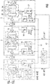
- FIG shows a basic arrangement of an optical wavelength path in an optical network transmitting a channel test signal.
- FIG illustrates an optical fiber link. Only two spans of an optical network for transmitting a WDM-signal [ W avelength D ivision M ultiplex] WS are shown for reasons of clarity.
- a start node 1 is connected via a first optical fiber 2 to an intermediate node 3 (only one of a plurality of intermediate nodes connected in series is shown).
- the intermediate node 3 is connected via a further optical fiber 4 with a last node 5.
- start, intermediate and last node refer to nodes of an optical wavelength path for a certain optical channel signal OC1 of the WDM-signal, beginning at the start node 1, where this optical channel signal OC1 is added to the WDM-signal (or where a channel test signal is generated) and transmitted along that path to a receiver 57 of the last node 5 where the regarded channel signal is dropped (or where channel tracing and power adjustment is finished). Only the necessary elements of the nodes for explaining the invention are shown.
- An embodiment of the start node 1 comprises one or more optical devices 11 with controllable VOA [variable optical attenuator] ability.
- These optical devices may comprise wavelength-de-multiplexers receiving WDM-signals (not shown in node 1), wavelength-multiplexers like 12, and discrete VOA-elements 16, 17,....
- Preferable optical devices are wavelength selective switches [WSS].
- the WS-switches comprise beside switching ability a separately controllable attenuation ability for each optical channel signal, in the figure FIG depicted as VOAs.
- a first optical channel signal OC1 is e.g. output by an optical transmitter [TX] (transponder) 14. In this embodiment alternatively another optical channel signal OCX output by a second optical transmitter 15 could be added.
- the chosen optical channel signal OC1 is combined with a plurality of further channel signals OC2 - OCn to the WDM-signal WS as mentioned above, amplified by an optical booster (amplifier) 13, and transmitted via the first optical fiber 2.
- a measurement signal is branched of the WDM-signal at the input of the booster 13 and converted by an optical-electrical converter (photo diode) 18 into an electrical measurement signal EM1.
- the VOA function preferable of the WSS 11 (or/and the optical transmitter 14 or WSS 12), depicted as VOA 16, is used for modulating the optical channel signal OC1 with a modulation test signal MT1 to be traced and/or adjusted. Only this channel signal is regarded for explaining the invention.
- the channel signal is an un-modulated optical carrier or already modulated with a data signal, and in an operating state the channel signal is usually a data signal.
- This signal is on-off modulated e.g. with a low frequency modulation test signal, e.g. a 1010-signal or a special channel signature generating said optical channel test signal, referred to as channel test signal OT1 with an amplitude of the optical channel signal OC1.
- a channel signature a consecutively repeated channel number, preferably an equal weight codeword, or a CDMA [Code Division Multiple Access] codeword [chip] may be used.
- the generated channel test signal OT1 is - as the channel signal OC1 before - wavelength multiplexed with said further optical channel signals OC2-OCn and then transmitted as WDM-signal WS via the optical fiber 2 to the next downstream intermediate node 3.
- the intermediate node 3 comprises a pre-amplifier 31 receiving the WDM-signal WS (the same name is used for the WDM-signal transmitted along the shown path, even if some channels may be dropped or added), one optical device 32-35 - preferable a WSS circuit (or a plurality of devices), and a booster 36.
- the function of the WSS is depicted as combination of a de-multiplexer 32, VOAs 33, 34, ..., and a multiplexer 35. In the node some received channel signals may be dropped and new channel signals may be added via a further optical transmitter 38.
- the output WDM-signal comprising the regarded channel signal OC1 or the channel test signal OT1 respectively is transmitted via the further optical fiber 4 and via further intermediate nodes (not shown) to the last node 5.
- Optical-electrical converters (photo diodes) 37 and 39 are connected to an input (or output) of the pre-amplifier 31 and the output (or input) of the booster 36 outputting electrical measurement signals EM2 and EM3.
- the arrangement of the last node 5 complies with the arrangement of the intermediate node. It comprises a pre-amplifier 51, an optical device, WSS, 52-54, an output booster 55, an optical-electrical converter 56 connected to an input (or output) of the pre-amplifier 51, and a channel receiver [RX] 57.
- the regarded optical channel signal OC1 is fed to said receiver 57 representing an end of the regarded signal path.
- the optical-electrical converters in all nodes are already components of gain controls of the amplifiers 13, 31, 36, 51.
- the shown amplifiers are regarded as constant gain controlled. Of course, additional functions as setting the gain control or tilt may be also implemented.
- the electrical measurement signals EM2, EM3, EM4 are derived from the received optical WDM-signal WS and may be tapped at power monitoring ports 40, 41, 58 of the downstream nodes 3 and 5.
- Each tapped measurement signal EM2, EM3 and EM4 is correlated with a correlation signal MC1 which corresponds to the modulation test signal MT1 of the regarded channel test signal OT1.
- the modulation test signal MT1 is detected e.g. by recognizing a certain clock signal or a channel signature and the channel test signal OT1 can by reliably traced.
- the attenuations of the VOAs are first set to high values and the estimated low output power values are checked before the predetermined low values are adjusted.
- adjusting of output power levels of the channel signals is considered.
- the output power levels of the start node are adjusted.
- the power levels of channel signals OC1,-OCn have to be derived from the WDM-signal without complex equipment.
- a wavelength de-multiplexer is not necessary.
- only the power level adjustment of the first channel signal OC1 is regarded.
- a channel test signal OT1 is generated in the start node 1 first.
- a measurement signal is branched off the WDM-signal WS at the input (or output) of the constant gain controlled booster 13, and converted by the optical-electrical converter 18 into the electrical measurement signal EM1 (output power monitoring port 19).
- This measurement signal EM1 is correlated with a correlation signal MC1 in a service device 6 for obtaining the channel output power level PC1 of said channel test signal OT1.
- a sufficient long correlation period is necessary to achieve reliable results.
- the amplitude of the regained low frequency modulation signal corresponds to the power level of the channel test signal OT1 and therefore to the power of the optical channel signal OC1.
- the obtained power level PC1 is compared with a target power value PT1 and the power level of the channel test signal OT1 is adjusted to said target power value PT1, e.g. by setting the attenuation of the VOA 16 in the path of the optical channel test signal.
- the necessary attenuation of the allocated VOA 16 is calculated and set (or e.g. output power of transmitter 14 is set).
- the power adjustment could be carried out in small steps.
- Another adjustment possibility is to compare the measured power level with the target power and to rise and decrease the attenuation/channel power level in small steps in a control loop till the target power PT1 is reached.
- the output power level of the channel test signal OT1 at the first downstream intermediate node 3 has to be adjusted.
- a measurement signal is derived (as an example only showing a second possibility) from the output signal of the booster 36 and converted by the optical-electrical converter 39.
- the output electrical measurement signal EM3 at output power monitoring port 41 is correlated with said correlation signal MC1, and an obtained channel output power level PC3 is compared with an allocated target value PT3. Then, according to the difference the output power level of the channel test signal OT1 is adjusted by setting the optical device 32-35.
- the channel output power levels of further downstream nodes are adjusted (the same reference signs are used for the signals WS and OT1 on their path from the start node to the last node).
- the adjustments can be carried out in a preferred second embodiment span by span (between two adjacent nodes or between respectively only few spans respectively).
- the output power level of the channel signal OC1 (or of a plurality of channel signals OC1 - OCn) output from the first node 1 is adjusted as described above. Then the optical channel signal OC1 is on-off modulated in the next downstream intermediate node 3 by the modulation test signal MT1 generating the channel test signal OT1 with high signal quality.
- the attenuation ability of the optical device/WSS 32-35 is in addition used for amplitude modulation avoiding additional complex arrangements, depicted in the figure as modulating VOA 34.
- the channel output power level PC3 of the channel test signal OT1 is again derived from the measurement signal branched off the WDM-signal WS at the output (or input) of the booster 36. The channel output power is adjusted as described above.
- the channel power adjustment is then repeated for further channels in the same node or/and at further downstream nodes respectively.
- modulation of a channel signal generating the channel test signal, deriving the allocated measurement signal, and adjustment of the channel output power level are always performed in the same node.
- the channel test signal OT1 is generated in the start node 1 and transmitted to the first downstream intermediate node 3.
- the power level of the channel test signal OT1 is reduced by the attenuation of the fiber 2 and further physical effects.
- a measurement signal EM2 (power monitoring point 40) corresponding to the WDM-signal WS is branched off at an input or output of the pre-amplifier 31. If the input is used, the power adjustment is possible without activating this amplifier.
- a channel input power level PC2 of the received channel test signal OT1 is obtained from the measurement signal EM2. This power level is compared with an allocated target power value PT2, and the output power level of the channel signal OT1/OC1 of the next upstream node (start node) 1 is set by controlling the output channel power, in this example the attenuation of the VOA 16.
- This adjustment routine is repeated for all downstream nodes and till the input power level at the last node 5 is adjusted.
- the input power level PC4 of the channel test signal OT1 is derived from the measurement signal EM4, output from the optical-electrical converter 56 at a power monitoring point 58.
- the input power level adjustment is performed by setting the attenuation of the optical device/WSS 32-35 (VOA34) of the previous upstream node 3 till an allocated target value PT4 of the received channel test signal OT1 and therefore channel signal OC1 is achieved.
- the channel signal OC1 is transmitted (the channel signals OC1-OCn respectively).
- the channel power adjustment may be repeated for all optical channel signals also span by span in the preferred second embodiment as described above.
- the channel test signal OT1 is then generated successively in the nodes 1 and 3 and transmitted to the next downstream node, where the measurement signal for obtaining the channel input power level is derived.
- the input power level is then adjusted by adjusting the signal attenuation of all or selected channel test signal in the next upstream node.
- the FIG shows also the already mentioned service device 6 for performing all the calculations described above.
- the measurements signals EM1-EM5 are transmitted via a first service channel 61 from the optical-electrical converters 18, 37, 39, 56 to the service device, and service commands AC1, AC3 are forwarded via a second service channel 62 to the nodes for adjusting the channel output power levels, e.g. by adjusting the attenuation of the WSSs. These signals may be transmitted as digital optical signals.
- the correlation of the measurement signals EM1-4 is depicted as ⁇ ME1-4 x MC1 and the comparison for each of the of the obtained power values with the allocated target values as PC1-4 - PT1-4.
- the modulation signals MT1, ... may also be forwarded with the control commands.
- the channel tracing and/or power adjustment may be automated. On the other hand, if only output power adjustment is necessary in a transmission system and the adjustments are done locally at the nodes, the service channels are not necessary.
Landscapes
- Engineering & Computer Science (AREA)
- Computer Networks & Wireless Communication (AREA)
- Signal Processing (AREA)
- Physics & Mathematics (AREA)
- Electromagnetism (AREA)
- Optical Communication System (AREA)
Claims (15)
- Verfahren zum Einrichten eines Kanals in einem optischen WDM-Netzwerk (1-5), welches ein Wellenlängenmultiplexsignal (WDM - Wavelength-Division-Multiplex-Signal) (WS) über optische Kanäle überträgt, das die folgenden Schritte umfasst:- Konfigurieren eines Signalpfades zwischen einem Startknoten (1) über mindestens einen dazwischenliegenden Knoten (3, ...) und einem letzten Knoten (5) für ein optisches Kanalsignal (CS1), welches in einem optischen Kanal des WDM-Signals (WS) übertragen wird,- An-Aus-Modulieren des optischen Kanalsignals (OC1) am Startknoten (1) mit einem Modulations-Testsignal (MT1), welches ein Kanaltestsignal (OT1) erzeugt,- Übertragen des Kanaltestsignals (OT1) über den optischen Kanal des WDM-Signals (WS),- Abgreifen eines elektrischen Messsignals (EM1, EM2), welches von dem WDM-Signal (WS) abgeleitet ist, an einem stromabwärtigen Überwachungsport (19, 40),- Ableiten eines Leistungspegels (PC1, PC2) des Kanaltestsignals (OT1), indem ein Korrelationsverfahren zwischen dem elektrischen Messsignal (EM1, EM2) und einem Korrelationssignal (MC1) angewendet wird, welches mit dem Modulationstestsignal (MT1) korrespondiert, während einer ausreichend langen Zeit,- Berechnen eines Steuerungsbefehls (AC1) aus der Differenz zwischen dem gemessenen Leistungspegel (PC1, PC2) und einem Zielleistungswert (PT1, PT2), der dem optischen Kanalsignal (OC1) an einem bestimmten Leistungsüberwachungspunkt (19, 40) zugewiesen ist,- Festlegen eines Ausgangsleistungspegels (PC1) des optischen Kanalsignals (OC1) in dem Startknoten (1) gemäß dem Steuerungsbefehl (AC1), um den zugewiesenen Zielleistungspegel (PT1, PT2) zu erhalten, und- Festlegen des Ausgangsleistungspegels (PC3, PC4, ...) des Kanalsignals (OC1) in weiter stromabwärts gelegenen Knoten (3, 5), um weitere zugewiesene Zielleistungswerte (PT4, PT5) an weiter stromabwärts gelegenen Leistungsüberwachungspunkten (41, 58) zu erhalten.
- Verfahren nach Anspruch 1, wobei zum Einstellen eines Kanalausgangsleistungspegels (PC1, Pc3) eines Ausgangskanalsignals (OC1)- das elektrische Messsignal (EM1, EM3) von einem emittierten WDM-Signal (WS) an einem Eingang oder einem Ausgang eines Verstärkers (12, 36) ermittelt und an einem zugewiesenen Ausgangsleistungsüberwachungsport (19, 41) abgegriffen wird, und- der Kanalausgangsleistungspegel (PC1, PC3) an demselben Knoten (1, 3) eingestellt wird, um den zugewiesenen Zielleistungswert (PT1, PT3) zu erhalten.
- Verfahren nach Anspruch 2, wobei zum Einstellen des Kanalausgangsleistungspegels (PC1, PC3) des Ausgangskanalsignals (OC1)- das optische Kanalsignal (OC1) an dem mindestens einen stromabwärtigen Knoten (3) durch das Modulationstestsignal (MT1), welches das Kanaltestsignal (OT1) erzeugt, moduliert wird, und- das elektrische Messsignal (EM4) von dem emittierten WDM-Signal an dem Eingang oder Ausgang des Verstärkers (36) abgeleitet und an dem zugewiesenen Ausgangsleistungsmessport (41) des selben Knotens (3) abgegriffen wird.
- Verfahren nach Anspruch 1, wobei zum Einstellen eines Kanaleingangsleistungspegels (PC2, PC4) eines empfangenen Kanalsignals (OC1)- das elektrische Messsignal (EM2, EM4) von einem empfangenen WDM-Signal (WS) an einem Eingang oder Ausgang eines Vorverstärkers (31, 51) abgeleitet wird und an einem zugewiesenen Eingangsleistungsüberwachungsport (40, 58) an dem mindestens einen stromabwärtigen Knoten (3, 5) abgegriffen wird, und- der Kanalausgangsleistungspegel (PC1, PC3) des Kanalsignals (OT1) an dem nächsten stromaufwärtigen Knoten (1, 3) eingestellt wird, um den zugewiesenen Zielleistungswert (PT2, PT4) zu erhalten.
- Verfahren nach Anspruch 4, wobei- das optische Kanalsignal (OC1) an dem mindestens einen stromabwärtigen Knoten (3) durch das Modulationstestsignal (MT1), welches das Kanaltestsignal (OT1) erzeugt, moduliert wird, und- das elektrische Messsignal (EM5) von dem empfangenen WDM-Signal (WS) an dem Eingang oder Ausgang des Vorverstärkers (51) an dem nächsten stromabwärtigen Knoten (5) abgeleitet wird.
- Verfahren nach einem der vorhergehenden Ansprüche, wobei das Einstellen des Ausgangsleistungspegels (PC1, PC3) oder des Eingangsleistungspegels (PC2, PC4) für alle Kanalsignale (OC1-OCn) eines Knoten (1, 3, 5) wiederholt wird.
- Verfahren nach Anspruch 1, wobei zum Kanalverfolgen und/oder für die Einrichtung des Systems die Ausgangsleistungspegel (PC1, PC3) der optischen Kanalsignale (OC1-OCn) und der Kanaltestsignale (OT1, ...) jeweils an dem Startknoten (1) bzw. den stromabwärtigen Knoten (3, 5) aus Sicherheitserwägungen auf einen vorbestimmten niedrigen Leistungspegel eingestellt werden.
- Verfahren nach einem der vorhergehenden Ansprüche, wobei das Modulationstestsignal (MT1) eine im Vergleich zur Datenrate eines optischen Kanalsignals (OC1) geringe Frequenz aufweist.
- Verfahren nach einem der vorhergehenden Ansprüche, wobei das Modulationstestsignal (MT1) einem Kanalidentifizierer entspricht.
- Verfahren nach Anspruch 9, wobei der Kanalidentifizierer ein Codewort gleichen Gewichts ("equal weight codeword") oder eine Code Division Multiple Access, CDMA, Chipsequenz ist.
- Verfahren nach einem der vorhergehenden Ansprüche, wobei- der Ausgangsleistungspegel des optischen Kanalsignals (OC1) oder des Kanaltestsignals (OT1) jeweils durch ein variables optisches Dämpfungsglied (variable optical attenuator, VOA) (16, 34) oder eine optische Einrichtung (11, 32-35) mit steuerbarer Dämpfungsfähigkeit eingestellt wird, und- die benötigte Dämpfung berechnet wird und der VOA (16, 34) oder die optische Einrichtung (11, 32-35) eingestellt wird, um den Zielleistungswert (PT1) zu erzielen.
- Verfahren nach einem der vorhergehenden Ansprüche, wobei die Ein-Aus-Modulation durch ein variables optisches Dämpfungsglied (variable optical attenuator, VOA) (16, 34) oder durch eine optische Einrichtung (11, 32-35) durchgeführt wird, die das Modulationstestsignal (MT1, ...) empfangen, und/oder
wobei ein optischer Träger oder ein optisches Datensignal durch das Modulationstestsignal (MT1) moduliert wird. - Verfahren nach einem der vorhergehenden Ansprüche, wobei- Steuerbefehle (AC1, AC3) und Messsignale (EM3, EM5) über Servicekanäle (61, 62) zwischen den Knoten (1, 3, 5) und einer Serviceeinrichtung (6) übertragen werden, und/oder- die Steuerbefehle (AC1, AC3) an der Serviceeinrichtung (6) berechnet werden.
- Verfahren nach einem der vorhergehenden Ansprüche, wobei
die Verstärkung und eine Kennlinienneigung (tilt) eines optischen Verstärkers (12, 31, 36, 51), der in den Knoten (1, 3, 5) enthalten ist, eingestellt wird, und/oder wobei die Messsignale (EM1-EM4) und/oder Steuerbefehle (AC1, AC3) und/oder die Modulationstestsignale (MT1, ...) zwischen einer Serviceeinrichtung und den Knoten (1, 3, 5) übertragen werden. - Anordnung zur Einrichtung einer Kanalleistung in einem optischen Netzwerk (1-5) welches optische Kanalsignale (OC1) in einem optischen Kanal eines Wellenlängenmultiplexsignals (WDM - Wavelength-Division-Multiplex-Signal) (WS) über einen optischen Pfad mit mindestens einem Startknoten (1), mindestens einem zwischenliegenden Knoten (3) und einem letzten Knoten (5) überträgt, wobei die Anordnung Folgendes umfasst:- Mittel zum Konfigurieren eines Signalpfades zwischen einem Startknoten (1), über mindestens einen zwischenliegenden Knoten (3, ...) und einem letzten Knoten (5) für ein optisches Kanalsignal (CS1), welches in einem optischen Kanal eines WDM-Signals (WS) übertragen wird;- Mittel (11; 16, 34) für das An-Aus-Modulieren des optischen Kanalsignals (OC1) an dem Startknoten (1) mit einem Modulationstestsignal (MT1), welches ein Kanaltestsignal (OT1) erzeugt;- Mittel zum Übertragen des Kanaltestsignals (OT1) über den optischen Kanal des WDM-Signals (WS),- Mittel zum Abgreifen eines elektrischen Messsignals (EM1, EM2), welches von dem WDM-Signal (WS) abgeleitet ist, an einem stromabwärtigen Überwachungsport (19, 40),- Mittel (6) zum Ableiten eines Leistungspegels (PC1, PC2) des Kanaltestsignals (OT1) durch Anwenden eines Korrelationsverfahrens zwischen dem elektrischen Messsignal (EM1, EM2) und einem Korrelationssignal (MC1), welches mit dem Modulationstestsignal (MT1) korrespondiert, während einer ausreichend langen Zeit,- Mittel (6) zum Berechnen eines Steuerbefehls (AC1) aus der Differenz zwischen dem gemessenen Leistungspegel (PC1, PC2) und einem Zielleistungswert (PT1, PT2), der dem optischen Kanalsignal (OC1) an einem bestimmten Leistungsüberwachungspunkt (19, 40) zugewiesen ist,- Mittel (11; 16, 34) zum Einstellen des Ausgangsleistungspegels (PC1) des optischen Kanalsignals (OC1) in dem Startknoten (1) gemäß dem Steuerbefehl (AC1), um den zugewiesenen Zielleistungswert (PT1, PT2) zu erhalten, und- Mittel (32-35, 52-54) zum Festlegen des Ausgangsleistungspegels (PC3, PC4, ...) des Kanalsignals (OC1) in weiteren stromabwärtigen Knoten (3, 5), um weitere zugewiesene Zielleistungswerte (PT4, PT5) an weiteren stromabwärtigen Leistungsüberwachungspunkten (41, 48) zu erhalten.
Applications Claiming Priority (1)
| Application Number | Priority Date | Filing Date | Title |
|---|---|---|---|
| PCT/EP2012/061753 WO2014015888A1 (en) | 2012-07-26 | 2012-07-26 | Method and arrangement for channel set up in an optical wdm-network |
Publications (2)
| Publication Number | Publication Date |
|---|---|
| EP2878089A1 EP2878089A1 (de) | 2015-06-03 |
| EP2878089B1 true EP2878089B1 (de) | 2018-10-24 |
Family
ID=46397203
Family Applications (1)
| Application Number | Title | Priority Date | Filing Date |
|---|---|---|---|
| EP12730458.2A Active EP2878089B1 (de) | 2012-07-26 | 2012-07-26 | Verfahren und anordnung für kanalaufbau in einem optischen wdm-netzwerk |
Country Status (4)
| Country | Link |
|---|---|
| US (1) | US9621261B2 (de) |
| EP (1) | EP2878089B1 (de) |
| CN (1) | CN104509010B (de) |
| WO (1) | WO2014015888A1 (de) |
Cited By (1)
| Publication number | Priority date | Publication date | Assignee | Title |
|---|---|---|---|---|
| US20210175972A1 (en) * | 2017-12-13 | 2021-06-10 | Telefonaktiebolaget Lm Ericsson (Publ) | Device and Method for Processing an Optical Signal |
Families Citing this family (10)
| Publication number | Priority date | Publication date | Assignee | Title |
|---|---|---|---|---|
| US9226751B2 (en) | 2012-06-28 | 2016-01-05 | Ethicon Endo-Surgery, Inc. | Surgical instrument system including replaceable end effectors |
| CN104509010B (zh) | 2012-07-26 | 2018-05-29 | 骁阳网络有限公司 | 用于光学wdm网络中信道建立的方法和装置 |
| CN106303765B (zh) * | 2015-05-26 | 2019-03-15 | 中兴通讯股份有限公司 | 一种分布式自动功率优化系统及方法 |
| US10484074B2 (en) * | 2015-08-25 | 2019-11-19 | Cellium Technologies, Ltd. | Systems and methods for maximizing data transmission rates in conjunction with a spatial-multiplexing transmission |
| US11303346B2 (en) | 2015-08-25 | 2022-04-12 | Cellium Technologies, Ltd. | Systems and methods for transporting signals inside vehicles |
| JP6103097B1 (ja) * | 2016-03-18 | 2017-03-29 | 日本電気株式会社 | 光伝送装置及びその制御方法 |
| CN106899373A (zh) * | 2017-04-26 | 2017-06-27 | 武汉光迅科技股份有限公司 | 一种带闭环光功率控制功能的波分复用器及控制方法 |
| JP7524631B2 (ja) * | 2020-06-29 | 2024-07-30 | 富士通株式会社 | 光受信装置及び光受信方法 |
| US11296791B1 (en) * | 2020-10-02 | 2022-04-05 | Cisco Technology, Inc. | Auto-tuneable optical transceiver modules |
| CN115250152A (zh) * | 2021-04-25 | 2022-10-28 | 富泰华工业(深圳)有限公司 | 终端测试方法、计算机装置及存储介质 |
Family Cites Families (13)
| Publication number | Priority date | Publication date | Assignee | Title |
|---|---|---|---|---|
| US5513029A (en) | 1994-06-16 | 1996-04-30 | Northern Telecom Limited | Method and apparatus for monitoring performance of optical transmission systems |
| US6043915A (en) * | 1997-03-31 | 2000-03-28 | Lucent Technologies Inc. | Stabilization of a multi-channel optical signal transmitter through correlation feedback |
| JP3779502B2 (ja) | 1999-08-12 | 2006-05-31 | 富士通株式会社 | 光増幅装置、光送信装置、光伝送システム、光増幅方法および光入射方法 |
| JP4234927B2 (ja) * | 2000-04-14 | 2009-03-04 | 富士通株式会社 | 光波長多重伝送システム及び光出力制御方法及び光波長多重伝送装置 |
| JP4495321B2 (ja) * | 2000-08-29 | 2010-07-07 | 富士通株式会社 | 光レベル制御方法 |
| US6735395B1 (en) * | 2000-09-29 | 2004-05-11 | Futurewei Technologies, Inc. | WDM communication system utilizing WDM optical sources with stabilized wavelengths and light intensity and method for stabilization thereof |
| US6891995B2 (en) * | 2002-03-01 | 2005-05-10 | Matsushita Electric Industrial Co., Ltd. | Wavelength division multiplex transmission system |
| US7139486B2 (en) * | 2002-12-05 | 2006-11-21 | Tropic Networks Inc. | Method and apparatus for optical add/drop multiplexing in optical networks |
| WO2004107625A1 (en) | 2003-06-02 | 2004-12-09 | Tropic Networks Inc. | Method and system for identification of channels in an optical network |
| JP4176061B2 (ja) | 2004-08-03 | 2008-11-05 | 富士通株式会社 | 光ネットワークシステム |
| US7715710B2 (en) * | 2006-05-30 | 2010-05-11 | Alcatel Lucent | Method and system for power management in optical networks |
| JP5633266B2 (ja) * | 2010-09-15 | 2014-12-03 | 富士通株式会社 | Wdm光伝送システムおよびその制御方法 |
| CN104509010B (zh) | 2012-07-26 | 2018-05-29 | 骁阳网络有限公司 | 用于光学wdm网络中信道建立的方法和装置 |
-
2012
- 2012-07-26 CN CN201280074476.9A patent/CN104509010B/zh active Active
- 2012-07-26 WO PCT/EP2012/061753 patent/WO2014015888A1/en not_active Ceased
- 2012-07-26 EP EP12730458.2A patent/EP2878089B1/de active Active
- 2012-07-26 US US14/410,907 patent/US9621261B2/en active Active
Non-Patent Citations (1)
| Title |
|---|
| None * |
Cited By (2)
| Publication number | Priority date | Publication date | Assignee | Title |
|---|---|---|---|---|
| US20210175972A1 (en) * | 2017-12-13 | 2021-06-10 | Telefonaktiebolaget Lm Ericsson (Publ) | Device and Method for Processing an Optical Signal |
| US11811455B2 (en) * | 2017-12-13 | 2023-11-07 | Telefonaktiebolaget Lm Ericsson (Publ) | Device and method for processing an optical signal |
Also Published As
| Publication number | Publication date |
|---|---|
| US9621261B2 (en) | 2017-04-11 |
| US20150256252A1 (en) | 2015-09-10 |
| EP2878089A1 (de) | 2015-06-03 |
| CN104509010B (zh) | 2018-05-29 |
| WO2014015888A1 (en) | 2014-01-30 |
| CN104509010A (zh) | 2015-04-08 |
Similar Documents
| Publication | Publication Date | Title |
|---|---|---|
| EP2878089B1 (de) | Verfahren und anordnung für kanalaufbau in einem optischen wdm-netzwerk | |
| JP4499576B2 (ja) | 光波長多重システム、光終端装置および光ネットワークユニット | |
| US9503186B2 (en) | Space division multiplexing apparatus including multi-core fiber and selfhomodyne detection method | |
| US6765659B1 (en) | Optical supervisory channel apparatus and method for measuring optical properties | |
| US6574016B1 (en) | Method and apparatus for ancillary data in a wavelength division multiplexed system | |
| US20170155981A1 (en) | Optical transmission device and optical transmission system | |
| EP2806583B1 (de) | Glasfaserübertragungssystem | |
| CN101455005A (zh) | 用于光网络中功率管理的方法和系统 | |
| US9438343B2 (en) | Transmitting device, communication system, and method for transmission level control | |
| WO2019151067A1 (ja) | 光伝送装置、伝送システム、及び伝送システムの制御方法 | |
| US20240022346A1 (en) | Optical transceiver and method for automatically setting wavelength thereof | |
| US11309973B2 (en) | Optical burst monitoring | |
| EP2999151B1 (de) | Verfahren und Kommunikationssteuervorrichtung zum Aufbauen eines Kommunikationskanals in einem Kommunikationsnetz | |
| US11646791B2 (en) | Passive optical network systems | |
| US20120318965A1 (en) | Optical transmission system and optical transmission method | |
| US20050259264A1 (en) | Observation apparatus and observation system | |
| EP1514372B1 (de) | Leistungsoptimierung in optischen kommunikationsnetzwerken | |
| KR100845412B1 (ko) | 톤주파수를 사용하는 파장분할다중 가입자망 | |
| US20240154691A1 (en) | Optical control device, optical transmission device, and signal light setting method | |
| WO2025247548A1 (en) | Method of wavelength-division multiplexing | |
| WO2025247546A1 (en) | Improvements to wavelength-division multiplexing | |
| KR20080061341A (ko) | 톤주파수를 이용하여 채널을 구별하는 파장분할다중가입자망 |
Legal Events
| Date | Code | Title | Description |
|---|---|---|---|
| PUAI | Public reference made under article 153(3) epc to a published international application that has entered the european phase |
Free format text: ORIGINAL CODE: 0009012 |
|
| 17P | Request for examination filed |
Effective date: 20141219 |
|
| AK | Designated contracting states |
Kind code of ref document: A1 Designated state(s): AL AT BE BG CH CY CZ DE DK EE ES FI FR GB GR HR HU IE IS IT LI LT LU LV MC MK MT NL NO PL PT RO RS SE SI SK SM TR |
|
| AX | Request for extension of the european patent |
Extension state: BA ME |
|
| RAP1 | Party data changed (applicant data changed or rights of an application transferred) |
Owner name: XIEON NETWORKS S.A R.L. |
|
| DAX | Request for extension of the european patent (deleted) | ||
| STAA | Information on the status of an ep patent application or granted ep patent |
Free format text: STATUS: EXAMINATION IS IN PROGRESS |
|
| 17Q | First examination report despatched |
Effective date: 20170810 |
|
| RIC1 | Information provided on ipc code assigned before grant |
Ipc: H04J 14/02 20060101AFI20180322BHEP Ipc: H04B 10/077 20130101ALI20180322BHEP |
|
| GRAP | Despatch of communication of intention to grant a patent |
Free format text: ORIGINAL CODE: EPIDOSNIGR1 |
|
| STAA | Information on the status of an ep patent application or granted ep patent |
Free format text: STATUS: GRANT OF PATENT IS INTENDED |
|
| INTG | Intention to grant announced |
Effective date: 20180503 |
|
| GRAS | Grant fee paid |
Free format text: ORIGINAL CODE: EPIDOSNIGR3 |
|
| GRAA | (expected) grant |
Free format text: ORIGINAL CODE: 0009210 |
|
| STAA | Information on the status of an ep patent application or granted ep patent |
Free format text: STATUS: THE PATENT HAS BEEN GRANTED |
|
| AK | Designated contracting states |
Kind code of ref document: B1 Designated state(s): AL AT BE BG CH CY CZ DE DK EE ES FI FR GB GR HR HU IE IS IT LI LT LU LV MC MK MT NL NO PL PT RO RS SE SI SK SM TR |
|
| REG | Reference to a national code |
Ref country code: GB Ref legal event code: FG4D |
|
| REG | Reference to a national code |
Ref country code: CH Ref legal event code: EP |
|
| REG | Reference to a national code |
Ref country code: IE Ref legal event code: FG4D |
|
| REG | Reference to a national code |
Ref country code: AT Ref legal event code: REF Ref document number: 1057944 Country of ref document: AT Kind code of ref document: T Effective date: 20181115 |
|
| REG | Reference to a national code |
Ref country code: DE Ref legal event code: R096 Ref document number: 602012052570 Country of ref document: DE |
|
| REG | Reference to a national code |
Ref country code: NL Ref legal event code: MP Effective date: 20181024 |
|
| REG | Reference to a national code |
Ref country code: LT Ref legal event code: MG4D |
|
| REG | Reference to a national code |
Ref country code: AT Ref legal event code: MK05 Ref document number: 1057944 Country of ref document: AT Kind code of ref document: T Effective date: 20181024 |
|
| PG25 | Lapsed in a contracting state [announced via postgrant information from national office to epo] |
Ref country code: NL Free format text: LAPSE BECAUSE OF FAILURE TO SUBMIT A TRANSLATION OF THE DESCRIPTION OR TO PAY THE FEE WITHIN THE PRESCRIBED TIME-LIMIT Effective date: 20181024 |
|
| PG25 | Lapsed in a contracting state [announced via postgrant information from national office to epo] |
Ref country code: ES Free format text: LAPSE BECAUSE OF FAILURE TO SUBMIT A TRANSLATION OF THE DESCRIPTION OR TO PAY THE FEE WITHIN THE PRESCRIBED TIME-LIMIT Effective date: 20181024 Ref country code: BG Free format text: LAPSE BECAUSE OF FAILURE TO SUBMIT A TRANSLATION OF THE DESCRIPTION OR TO PAY THE FEE WITHIN THE PRESCRIBED TIME-LIMIT Effective date: 20190124 Ref country code: PL Free format text: LAPSE BECAUSE OF FAILURE TO SUBMIT A TRANSLATION OF THE DESCRIPTION OR TO PAY THE FEE WITHIN THE PRESCRIBED TIME-LIMIT Effective date: 20181024 Ref country code: HR Free format text: LAPSE BECAUSE OF FAILURE TO SUBMIT A TRANSLATION OF THE DESCRIPTION OR TO PAY THE FEE WITHIN THE PRESCRIBED TIME-LIMIT Effective date: 20181024 Ref country code: LT Free format text: LAPSE BECAUSE OF FAILURE TO SUBMIT A TRANSLATION OF THE DESCRIPTION OR TO PAY THE FEE WITHIN THE PRESCRIBED TIME-LIMIT Effective date: 20181024 Ref country code: LV Free format text: LAPSE BECAUSE OF FAILURE TO SUBMIT A TRANSLATION OF THE DESCRIPTION OR TO PAY THE FEE WITHIN THE PRESCRIBED TIME-LIMIT Effective date: 20181024 Ref country code: NO Free format text: LAPSE BECAUSE OF FAILURE TO SUBMIT A TRANSLATION OF THE DESCRIPTION OR TO PAY THE FEE WITHIN THE PRESCRIBED TIME-LIMIT Effective date: 20190124 Ref country code: IS Free format text: LAPSE BECAUSE OF FAILURE TO SUBMIT A TRANSLATION OF THE DESCRIPTION OR TO PAY THE FEE WITHIN THE PRESCRIBED TIME-LIMIT Effective date: 20190224 Ref country code: FI Free format text: LAPSE BECAUSE OF FAILURE TO SUBMIT A TRANSLATION OF THE DESCRIPTION OR TO PAY THE FEE WITHIN THE PRESCRIBED TIME-LIMIT Effective date: 20181024 Ref country code: AT Free format text: LAPSE BECAUSE OF FAILURE TO SUBMIT A TRANSLATION OF THE DESCRIPTION OR TO PAY THE FEE WITHIN THE PRESCRIBED TIME-LIMIT Effective date: 20181024 |
|
| PG25 | Lapsed in a contracting state [announced via postgrant information from national office to epo] |
Ref country code: SE Free format text: LAPSE BECAUSE OF FAILURE TO SUBMIT A TRANSLATION OF THE DESCRIPTION OR TO PAY THE FEE WITHIN THE PRESCRIBED TIME-LIMIT Effective date: 20181024 Ref country code: PT Free format text: LAPSE BECAUSE OF FAILURE TO SUBMIT A TRANSLATION OF THE DESCRIPTION OR TO PAY THE FEE WITHIN THE PRESCRIBED TIME-LIMIT Effective date: 20190224 Ref country code: AL Free format text: LAPSE BECAUSE OF FAILURE TO SUBMIT A TRANSLATION OF THE DESCRIPTION OR TO PAY THE FEE WITHIN THE PRESCRIBED TIME-LIMIT Effective date: 20181024 Ref country code: RS Free format text: LAPSE BECAUSE OF FAILURE TO SUBMIT A TRANSLATION OF THE DESCRIPTION OR TO PAY THE FEE WITHIN THE PRESCRIBED TIME-LIMIT Effective date: 20181024 Ref country code: GR Free format text: LAPSE BECAUSE OF FAILURE TO SUBMIT A TRANSLATION OF THE DESCRIPTION OR TO PAY THE FEE WITHIN THE PRESCRIBED TIME-LIMIT Effective date: 20190125 |
|
| REG | Reference to a national code |
Ref country code: DE Ref legal event code: R097 Ref document number: 602012052570 Country of ref document: DE |
|
| PG25 | Lapsed in a contracting state [announced via postgrant information from national office to epo] |
Ref country code: CZ Free format text: LAPSE BECAUSE OF FAILURE TO SUBMIT A TRANSLATION OF THE DESCRIPTION OR TO PAY THE FEE WITHIN THE PRESCRIBED TIME-LIMIT Effective date: 20181024 Ref country code: DK Free format text: LAPSE BECAUSE OF FAILURE TO SUBMIT A TRANSLATION OF THE DESCRIPTION OR TO PAY THE FEE WITHIN THE PRESCRIBED TIME-LIMIT Effective date: 20181024 Ref country code: IT Free format text: LAPSE BECAUSE OF FAILURE TO SUBMIT A TRANSLATION OF THE DESCRIPTION OR TO PAY THE FEE WITHIN THE PRESCRIBED TIME-LIMIT Effective date: 20181024 |
|
| PG25 | Lapsed in a contracting state [announced via postgrant information from national office to epo] |
Ref country code: SK Free format text: LAPSE BECAUSE OF FAILURE TO SUBMIT A TRANSLATION OF THE DESCRIPTION OR TO PAY THE FEE WITHIN THE PRESCRIBED TIME-LIMIT Effective date: 20181024 Ref country code: RO Free format text: LAPSE BECAUSE OF FAILURE TO SUBMIT A TRANSLATION OF THE DESCRIPTION OR TO PAY THE FEE WITHIN THE PRESCRIBED TIME-LIMIT Effective date: 20181024 Ref country code: EE Free format text: LAPSE BECAUSE OF FAILURE TO SUBMIT A TRANSLATION OF THE DESCRIPTION OR TO PAY THE FEE WITHIN THE PRESCRIBED TIME-LIMIT Effective date: 20181024 Ref country code: SM Free format text: LAPSE BECAUSE OF FAILURE TO SUBMIT A TRANSLATION OF THE DESCRIPTION OR TO PAY THE FEE WITHIN THE PRESCRIBED TIME-LIMIT Effective date: 20181024 |
|
| PLBE | No opposition filed within time limit |
Free format text: ORIGINAL CODE: 0009261 |
|
| STAA | Information on the status of an ep patent application or granted ep patent |
Free format text: STATUS: NO OPPOSITION FILED WITHIN TIME LIMIT |
|
| 26N | No opposition filed |
Effective date: 20190725 |
|
| PG25 | Lapsed in a contracting state [announced via postgrant information from national office to epo] |
Ref country code: SI Free format text: LAPSE BECAUSE OF FAILURE TO SUBMIT A TRANSLATION OF THE DESCRIPTION OR TO PAY THE FEE WITHIN THE PRESCRIBED TIME-LIMIT Effective date: 20181024 |
|
| PG25 | Lapsed in a contracting state [announced via postgrant information from national office to epo] |
Ref country code: MC Free format text: LAPSE BECAUSE OF FAILURE TO SUBMIT A TRANSLATION OF THE DESCRIPTION OR TO PAY THE FEE WITHIN THE PRESCRIBED TIME-LIMIT Effective date: 20181024 |
|
| REG | Reference to a national code |
Ref country code: CH Ref legal event code: PL |
|
| GBPC | Gb: european patent ceased through non-payment of renewal fee |
Effective date: 20190726 |
|
| PG25 | Lapsed in a contracting state [announced via postgrant information from national office to epo] |
Ref country code: TR Free format text: LAPSE BECAUSE OF FAILURE TO SUBMIT A TRANSLATION OF THE DESCRIPTION OR TO PAY THE FEE WITHIN THE PRESCRIBED TIME-LIMIT Effective date: 20181024 |
|
| REG | Reference to a national code |
Ref country code: BE Ref legal event code: MM Effective date: 20190731 |
|
| PG25 | Lapsed in a contracting state [announced via postgrant information from national office to epo] |
Ref country code: GB Free format text: LAPSE BECAUSE OF NON-PAYMENT OF DUE FEES Effective date: 20190726 |
|
| PG25 | Lapsed in a contracting state [announced via postgrant information from national office to epo] |
Ref country code: CH Free format text: LAPSE BECAUSE OF NON-PAYMENT OF DUE FEES Effective date: 20190731 Ref country code: LU Free format text: LAPSE BECAUSE OF NON-PAYMENT OF DUE FEES Effective date: 20190726 Ref country code: BE Free format text: LAPSE BECAUSE OF NON-PAYMENT OF DUE FEES Effective date: 20190731 Ref country code: LI Free format text: LAPSE BECAUSE OF NON-PAYMENT OF DUE FEES Effective date: 20190731 |
|
| PG25 | Lapsed in a contracting state [announced via postgrant information from national office to epo] |
Ref country code: FR Free format text: LAPSE BECAUSE OF NON-PAYMENT OF DUE FEES Effective date: 20190731 |
|
| PG25 | Lapsed in a contracting state [announced via postgrant information from national office to epo] |
Ref country code: IE Free format text: LAPSE BECAUSE OF NON-PAYMENT OF DUE FEES Effective date: 20190726 |
|
| PG25 | Lapsed in a contracting state [announced via postgrant information from national office to epo] |
Ref country code: CY Free format text: LAPSE BECAUSE OF FAILURE TO SUBMIT A TRANSLATION OF THE DESCRIPTION OR TO PAY THE FEE WITHIN THE PRESCRIBED TIME-LIMIT Effective date: 20181024 |
|
| PG25 | Lapsed in a contracting state [announced via postgrant information from national office to epo] |
Ref country code: MT Free format text: LAPSE BECAUSE OF FAILURE TO SUBMIT A TRANSLATION OF THE DESCRIPTION OR TO PAY THE FEE WITHIN THE PRESCRIBED TIME-LIMIT Effective date: 20181024 Ref country code: HU Free format text: LAPSE BECAUSE OF FAILURE TO SUBMIT A TRANSLATION OF THE DESCRIPTION OR TO PAY THE FEE WITHIN THE PRESCRIBED TIME-LIMIT; INVALID AB INITIO Effective date: 20120726 |
|
| PG25 | Lapsed in a contracting state [announced via postgrant information from national office to epo] |
Ref country code: MK Free format text: LAPSE BECAUSE OF FAILURE TO SUBMIT A TRANSLATION OF THE DESCRIPTION OR TO PAY THE FEE WITHIN THE PRESCRIBED TIME-LIMIT Effective date: 20181024 |
|
| PGFP | Annual fee paid to national office [announced via postgrant information from national office to epo] |
Ref country code: DE Payment date: 20250722 Year of fee payment: 14 |