EP2880764B1 - Verfahren und system zur monolithischen integration von schaltungen zur überwachung und steuerung von rf-signalen - Google Patents
Verfahren und system zur monolithischen integration von schaltungen zur überwachung und steuerung von rf-signalen Download PDFInfo
- Publication number
- EP2880764B1 EP2880764B1 EP13827857.7A EP13827857A EP2880764B1 EP 2880764 B1 EP2880764 B1 EP 2880764B1 EP 13827857 A EP13827857 A EP 13827857A EP 2880764 B1 EP2880764 B1 EP 2880764B1
- Authority
- EP
- European Patent Office
- Prior art keywords
- output
- modulator
- mzm
- arm
- signal
- Prior art date
- Legal status (The legal status is an assumption and is not a legal conclusion. Google has not performed a legal analysis and makes no representation as to the accuracy of the status listed.)
- Active
Links
Images






Classifications
-
- H—ELECTRICITY
- H04—ELECTRIC COMMUNICATION TECHNIQUE
- H04B—TRANSMISSION
- H04B10/00—Transmission systems employing electromagnetic waves other than radio-waves, e.g. infrared, visible or ultraviolet light, or employing corpuscular radiation, e.g. quantum communication
- H04B10/50—Transmitters
- H04B10/516—Details of coding or modulation
- H04B10/548—Phase or frequency modulation
- H04B10/556—Digital modulation, e.g. differential phase shift keying [DPSK] or frequency shift keying [FSK]
- H04B10/5561—Digital phase modulation
-
- H—ELECTRICITY
- H04—ELECTRIC COMMUNICATION TECHNIQUE
- H04B—TRANSMISSION
- H04B10/00—Transmission systems employing electromagnetic waves other than radio-waves, e.g. infrared, visible or ultraviolet light, or employing corpuscular radiation, e.g. quantum communication
- H04B10/07—Arrangements for monitoring or testing transmission systems; Arrangements for fault measurement of transmission systems
- H04B10/075—Arrangements for monitoring or testing transmission systems; Arrangements for fault measurement of transmission systems using an in-service signal
- H04B10/079—Arrangements for monitoring or testing transmission systems; Arrangements for fault measurement of transmission systems using an in-service signal using measurements of the data signal
- H04B10/0795—Performance monitoring; Measurement of transmission parameters
- H04B10/07955—Monitoring or measuring power
-
- H—ELECTRICITY
- H04—ELECTRIC COMMUNICATION TECHNIQUE
- H04B—TRANSMISSION
- H04B10/00—Transmission systems employing electromagnetic waves other than radio-waves, e.g. infrared, visible or ultraviolet light, or employing corpuscular radiation, e.g. quantum communication
- H04B10/50—Transmitters
- H04B10/501—Structural aspects
- H04B10/503—Laser transmitters
- H04B10/505—Laser transmitters using external modulation
- H04B10/5053—Laser transmitters using external modulation using a parallel, i.e. shunt, combination of modulators
-
- H—ELECTRICITY
- H04—ELECTRIC COMMUNICATION TECHNIQUE
- H04B—TRANSMISSION
- H04B10/00—Transmission systems employing electromagnetic waves other than radio-waves, e.g. infrared, visible or ultraviolet light, or employing corpuscular radiation, e.g. quantum communication
- H04B10/50—Transmitters
- H04B10/564—Power control
-
- H—ELECTRICITY
- H04—ELECTRIC COMMUNICATION TECHNIQUE
- H04J—MULTIPLEX COMMUNICATION
- H04J14/00—Optical multiplex systems
- H04J14/02—Wavelength-division multiplex systems
- H04J14/0227—Operation, administration, maintenance or provisioning [OAMP] of WDM networks, e.g. media access, routing or wavelength allocation
-
- H—ELECTRICITY
- H04—ELECTRIC COMMUNICATION TECHNIQUE
- H04L—TRANSMISSION OF DIGITAL INFORMATION, e.g. TELEGRAPHIC COMMUNICATION
- H04L27/00—Modulated-carrier systems
- H04L27/18—Phase-modulated carrier systems, i.e. using phase-shift keying
- H04L27/20—Modulator circuits; Transmitter circuits
- H04L27/2096—Arrangements for directly or externally modulating an optical carrier
Definitions
- EP 2 003 486 A2 relates to a quadrature phase shift keying modulator having a structure such that the average light output power of phase-shift keying modulation light output from a combining unit is changed according to the phase difference between the first and the second optical signal after being combined by means of applying driving signals different in eye crossing percentage by a first modulator and a second modulator, respectively.
- the quadrature phase shift keying modulator further has a power monitor monitoring the average light output power of quadrature phase-shift keying modulated light and a phase shift controlling unit which performs feedback control of the phase shift amount in the phase shifting unit based on the average light output power monitored by the power monitor.
- US 2010/0142964 A1 discloses an optical transmission apparatus for high-speed optical signal transmission, which includes an optical modulator which having first and second modulators of a Mach-Zehnder (MZ) interferometer type, connected in parallel, and an output stabilizer which controls biases for the first modulator, the second modulator and the optical modulator and stabilizes a final output optical signal of the optical modulator.
- MZ Mach-Zehnder
- US 2009/0162052 A1 relates to a device for measuring optical latency in a test path, including an optical source to generate an optical signal.
- An optical modulator modulates the optical signal based on a modulation signal.
- An output port outputs the modulated optical signal to the test path.
- An input port receives a return optical signal following propagation through the test path.
- Latency calculating logic calculates the optical latency for the test path based on the modulation signal and the return optical signal.
- US 2006/0029395 A1 discloses an optical transmission apparatus employing an FSK scheme and including a light generator arranged to generate a first tone signal having a first frequency and a second tone signal having a second frequency, and a light modulator including a second modulator for selectively outputting one of the first tone signal and the second tone signal input from the light generator according to input data.
- US 2003/0231725 A1 relates to methods and apparatus for performing spectral filtering of channel estimates corresponding to a communications channel used to transmit a multi-tone signal.
- a channel estimate is examined to identify portions where significant multi-path interference is present.
- Low pass filters are used to perform spectral filtering on the channel estimate to produce a filtered channel estimate.
- US 2006/0034616 A1 relates to an optical modulator which comprises a driver for providing an electrical data signal to the modulator and bias means for providing a bias voltage to the modulator.
- a microprocessor provides a low frequency digital modulation signal, which is converted to an analogue modulation signal by a digital to analogue converter.
- the analogue modulation signal is applied to the bias means or the driver.
- Intensity detection means are further provided for detecting the intensity of light emitted by the modulator.
- An analogue to digital converter converts the output of the intensity detection means to a digital intensity signal which is analyzed, and the bias means instructed to adjust the bias voltage on the basis of the analyzed signal.
- WO 2011/104838 A1 relates to an optical transmitter generating an arbitrary optical waveform including an analog optical waveform, which is capable of controlling a bias to a Null point easily.
- the optical transmitter includes: a light intensity detector detecting intensity of output light of the optical modulator; a data signal generator generating the data sequence; an average modulation degree calculator calculating an average modulation degree of the data sequence based on the data sequence; and a bias controller performing bias control on the optical modulator based on the intensity of the output light detected by the light intensity detector and the average modulation degree of the data sequence calculated by the average modulation degree calculator.
- US 2005/0117191 A1 relates to a modulator arrangement for modulating an optical signal using a quadrature phase shift key for use in an optical wavelength division multiplex (WDM) optical communications system
- WDM optical wavelength division multiplex
- a laser for producing an optical signal of a selected wavelength, which signal is split by a splitter, each part of said split signal being applied to a respective phase modulator each for which is adapted to modulate the phase of the signal in dependence on a respective drive voltages.
- the split signals being recombined by an optical recombiner to form an optical phase shift key output, wherein the output power is monitored by a detector, the detected signal then being used to drive a feedback arrangement to control electrodes of the phase modulators and/or phase shifter.
- Embodiments of the present invention relate to RF circuits. More particularly, embodiments of the present invention relate to an apparatus and method of integrating analog circuits (e.g., monolithic integration) used to monitor spectral information associated with RF signals, with particular applications in photonic integrated circuits.
- analog circuits e.g., monolithic integration
- monolithically integrated circuits are used to monitor and control RF signals.
- some implementations utilize analog circuits that are monolithically integrated and are used to monitor the spectrum of RF signals, providing novel control loops for optical phase shift keying modulation implementations.
- Some embodiments use analog circuits to filter out a portion of the spectrum (possibly of a digital signal) that is monitored, and then an analog circuit, such as a peak detector or RMS detector to monitor the power in real time.
- a method of operating a BPSK modulator includes receiving an RF signal at the BPSK modulator and splitting the RF signal into a first portion and a second portion that is inverted with respect to the first portion.
- the method also includes receiving the first portion at a first arm of the BPSK modulator, receiving the second portion at a second arm of the BPSK modulator, applying a first tone to the first arm of the BPSK modulator, and applying a second tone to the second arm of the BPSK modulator.
- the method further includes measuring a power associated with an output of the BPSK modulator and adjusting a phase applied to at least one of the first arm of the BPSK modulator or the second arm of the BPSK modulator in response to the measured power.
- a method of operating a QPSK modulator includes receiving an optical signal at a first BPSK modulator and generating a first modulated signal at an output of the first BPSK modulator.
- the method also includes receiving the optical signal at a second BPSK modulator and generating a second modulated signal at an output of the second BPSK modulator.
- the method further includes combining the first modulated signal and the second modulated signal at an output of the QPSK modulator, measuring a power associated with the output of the QPSK modulator, and adjusting a phase applied to the output of at least one of the first BPSK modulator or the second BPSK modulator in response to the measured power.
- a nested Mach-Zehnder modulator system includes an optical input port and an optical coupler coupled to the optical input port and having a first arm and a second arm.
- the nested Mach-Zehnder modulator system also includes a first inner Mach-Zehnder modulator (MZM) coupled to the first arm.
- the first inner MZM comprises a phase control section and an output.
- the nested Mach-Zehnder modulator system further includes a first optical detector coupled to the output of the first MZM, a feedback loop connecting the first optical detector to the phase control section, a second inner MZM coupled to the second arm and having a second phase control section and an output, and a second optical coupler receiving the output of the first MZM and the output of the second MZM.
- an apparatus includes a receiver coupled to a communications channel operable to carry an RF signal and a feedback loop coupled to a transmitter.
- the apparatus also includes an analog circuit coupled to the receiver and operable to monitor the RF signal.
- the analog circuit can include a spectral monitoring unit.
- the receiver can include a transceiver, which can be integrated in silicon photonics.
- the analog circuit includes a plurality of spectral filters characterized by a differing spectral bands and a plurality of RMS detectors, each of the RMS detectors being coupled to one of the plurality of spectral filters.
- a method includes receiving an RF signal at an input of a monolithically integrated analog circuit and measuring the RF signal using the monolithically integrated analog circuit. The method also includes providing a feedback signal based on the measured RF signal.
- the monolithically integrated analog circuit can include an RMS detector.
- measuring the RF signal comprises measuring a power associated with the RF signal in one or more predetermined spectral bands.
- the one or more predetermined spectral bands can be three spectral bands.
- embodiments of the present invention provide methods and systems that avoid heavy digital sampling and processing, which are associated with high power and cost.
- control loops for quadrature phase shift keying (QPSK) modulators are provided.
- QPSK quadrature phase shift keying
- embodiments of the present invention utilize analog circuits that can be monolithically integrated with photonic circuits, including silicon photonics, to monitor the RF signal and provide the desired feedback signal.
- FFT fast Fourier transform
- embodiments of the present invention reduce the computational complexity, power requirements, cost, and the like of integrated optoelectronics.
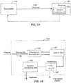
- FIG. 1A is a block diagram illustrating a communication system according to an embodiment of the present invention.
- the communications system provides methods and systems for signal monitoring and spectrum equalization.
- Transmitter 110 and receiver 120 are utilized in conjunction with communications channel 115.
- the spectral monitoring unit 122 included as part of the receiver 120 provides feedback on channel distortion to a transmitter 110, thereby allowing the transmitter to compensate for the channel distortion and correct the spectrum. Feedback from the spectral monitoring unit 122 is provided using feedback path 130 in the illustrated embodiment.
- an RF signal is monitored to detect channel distortion and provide feedback to a receiver, in order to equalize the signal spectrum.
- FIG. 1B is a simplified block diagram illustrating elements of receiver 120 according to an embodiment of the present invention.
- the receiver 120 e.g., an integrated optical receiver
- the Polarization Diversity Unit (e.g. splitter and rotator) 155 there can be two waveguides (e.g. for TE polarized light and TM light rotated to TE polarization).
- Optical filter 157 is illustrated, which can be a WDM filter.
- Light is detected by photodiode 165 and passed to spectral monitoring unit 160. It should be noted that there can be a plurality of waveguides and photodiodes.
- the methods and systems described herein can be used outside of optics (i.e., the channel does not have to be an optical channel). It should be appreciated that the elements illustrated in FIG. 1B are only exemplary and are not required by the present invention and can be utilized, replaced, or removed depending on the particular application.
- FIG. 2 is simplified block diagram of spectral monitoring unit according to an embodiment of the present invention.
- the spectral monitoring unit 200 includes a set of three spectral filters: low pass filter (LPF) 220, which passes frequencies less than 4 GHz; band pass filter (BPF) 222, which passes frequencies between 4 GHz and 8 GHz; and high pass filter (HPF) 224, which passes frequencies above 8 GHz.
- the spectral monitoring unit 200 also includes a set (e.g., three) RMS detectors 230, 232, and 234, which receive the outputs of the corresponding filters 220, 222, and 224, respectively. Utilizing the spectral monitoring unit 200, the distortion as a function of frequency can be measured and feedback can be provided to the transmitter to compensate for the distortion in the channel.
- a iow pass filter LPF
- the distorted signal is then provided as an input to the spectral monitoring unit 200, which can include a set (e.g., three) filters that pass predetermined bands.
- the spectral monitoring unit 200 can include a set (e.g., three) filters that pass predetermined bands.
- three filters 220, 222, and 224 can be utilized: low pass, bandpass, and high pass, but the present invention is not limited to this configuration.
- Other numbers of filters with predetermined spectral characteristics can be utilized, for example less than three filters or more than three filters.
- the outputs from the spectral filters are provided as inputs to a set of RMS detectors coupled to the filters, providing measurements of the power in each spectral band.
- the RMS detectors are illustrated as RMS detectors 230, 232, and 234.
- the outputs of the RMS detectors provide an indication of the distortion present in the spectrum, and thus can be used to provide feedback for compensation of the channel distortion.
- FIG. 3 is a plot illustrating filter frequency response curves according to an embodiment of the present invention.
- the LPF filters signals below 4 GHz
- the BPF filters signals between 4 and 8 GHz
- the HPF filters signals above 8 GHz.
- FIG. 4 is plot illustrating the frequency content of an input signal according to an embodiment of the present invention.
- this input signal which is associated with a 12 Gpbs PRBS signal, a dip can be seen in the spectrum at 12 GHz.
- the V RF_in shown in FIG. 2 is the voltage of a RF signal, and in particular it may be a pseudo random bit series (PRBS) at a desired bit rate (e.g., 12 Gbps), useful for demonstrating the operation of the methods and systems described herein.
- PRBS pseudo random bit series
- FIG. 5 is a plot illustrating simulated channel distortion according to an embodiment of the present invention. As illustrated in FIG. 5 , channel distortion can be modeled and/or simulated by a Low Pass Filter (LPF) with an attenuation of 10 dB between 1 GHz and 12 GHz.
- LPF Low Pass Filter
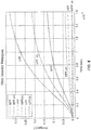
- FIG. 6 is a plot illustrating RMS detector response for various filters according to an embodiment of the present invention.
- the output of the set of RMS detectors is illustrated as "RMS Detector Response," showing the difference between the output, for example, of the low pass filter with no channel distortion (LPF) and the output of the low pass filter with the channel distortion applied (LPF ch).
- Curves for the other spectral filters show similar decreases in RMS detector output when channel distortion is introduced - BPF and BPF ch; HPF and HPF ch.
- the RMS detector output is lower for each of the filtered signals when channel distortion is included.
- the use of the analog detector e.g., an RMS detector to measure the output power in the various spectral bands enables a measurement of the impact of the introduction of channel distortion (represented by a decrease in output response in this example), which can then be used to provide a feedback signal to compensate for the channel distortion.
- the analog circuits can be monolithically integrated, they can be used in place of digital circuits that could be used to provide the feedback control signals.
- the received signal may be flat as a function of frequency, resulting in equal voltages at each of RMS detectors 230, 232, and 234.
- Attenuation at some frequencies can result in a decrease in the voltage measured at one or more of the RMS detectors (e.g., attenuation of low frequencies in comparison to high frequencies).
- the relative voltage decrease which is seen to be highest at the HPF, where the signal was attenuated the most, can provide data used in the feedback loop to the transmitter to compensate for the channel distortion and return the RMS voltages to a common level.
- embodiments provide spectral monitoring of a digital signal such that channel distortion can be detected and feedback provided for signal equalization.
- a PRBS at 12 Gbps is generated and represented by +/-0.15 V.
- the spectrum can be filtered, using analog filters, into three spectral bands.
- the signals, after filtering, are each passed to one of a set of RMS detectors, which are used to measure the power present in each spectral band. Assuming uniform signals as a function of frequency, if the signal is distorted by the channel, then the output power at each RMS detector will change. Thus, the distortion resulting from the channel will be detected and can be used to provide feedback for the equalization of the signal at transmission.
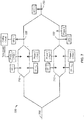
- FIG. 7 is a simplified schematic diagram illustrating a nested modulator system according to an embodiment of the present invention.
- This nested modulator system allows for control of null bias in an optical Mach-Zehnder Modulator (MZM) as described below.
- MZM optical Mach-Zehnder Modulator
- this control technique can be used to maintain the null bias in a Binary Phase Shift Keying (BPSK) modulation format.
- BPSK Binary Phase Shift Keying
- this control technique can be used for the inner modulators in a nested MZM configuration for QPSK, DQPSK, or DP-QPSK.
- BPSK Binary Phase Shift Keying
- the nested MZM configuration includes two inner MZMs, first MZM 710 and second MZM 712 connected together within an outer MZM 700.
- MZM 700 includes an input port 705 and an output port at node 730.
- each MZM uses a specific bias point for operation: The bias point of the inner MZMs 710 and 712 is maintained such that the output of the inner MZMs when the arms are not driven otherwise, is a minimum (null bias).
- the two high-speed RF inputs e.g. RF-I and RF-I bar
- drive the two arms e.g. with diodes
- the bias point of the outer MZM 700 is maintained such that the output of the inner MZMs are 90° out of phase (i.e., ⁇ /2) with one another (quadrature bias), as discussed below.
- the control loop for null bias relies on the application of two pilot tones that produce intermodulation tones in the output signal of the MZM.
- a peak detector analog circuit is then used to monitor the intensity of the odd intermodulation frequencies, and provide the feedback to maximize this quantity and maintain the null bias.
- the first inner MZM 710 receives I and I bar signals and the second inner MZM 712 receives the Q and Q bar signals for the 1 and Q constellation of the QPSK.
- Phase control is provided to each inner MZM and is illustrated by Phase 1 + Pilot 1 / Phase 2 + Pilot 2 provide to the upper and lower arms of the inner MZMs as shown in FIG. 7 .
- the power at node 720 is measured using monolithically integrated monitor photodetector (MPD 1), the power at node 722 is measured using MPD2, and the power at node 730 is measured using MPD3.
- Phase 3 is used to modify the phase of the lower arm of the outer MZM 700.
- phase adjustment devices can be utilized including heaters integrated with waveguide elements, electro-optic phase adjustment elements including diode-based phase adjustment sections, and the like. It is understood that in each case, only the phase difference between the two arms is of importance, and the actual phase shifters can be applied to one or both of the arms of each MZ (inner or outer).
- FIG. 8A is a plot illustrating spectral content measured at a detector according to an embodiment of the present invention.
- Pilot Tone 1 (f 1 ) was set at 3 kHz and Pilot Tone 2 (f 2 ) was set at 4 kHz.
- FIG. 8A shows the spectrum measured at MPD1, with peaks in the power spectrum at 2f 1 (6 kHz), 2f 2 (8 kHz), f 1 + f 2 (7 kHz), and f 1 - f 2 (1 kHz).
- FIG. 8B is a plot illustrating power as a function of modulator bias according to an embodiment of the present invention.
- FIG. 8B displays the inter-modulation power at f 1 - f 2 , which is related to the nonlinear transfer function of the MZM.
- a feedback signal is provided that can be used to control-loop the phase shift, preferably at ⁇ in this example.
- the phase can be adjusted until the inter-modulation spectrum is maximized, providing the desired null ( ⁇ ) bias point.
- power measurements are made using the MPD 1 and MPD 2 (which detect intensity) to determine that a ⁇ phase shift is present between the two arms of each MZM 710 and 712.
- MPD1 is used to control MZM 710 by measuring the power at the inter-modutation frequency of 1 kHz.
- 3 kHz and 4 kHz are utilized for the pilot tones in this example, the present invention is not limited to these frequencies and other suitable frequencies can be utilized as appropriate to the particular application.
- the pilot tones can be applied to separate arms or can be applied to the same arm.
- the power measured at MPD 2 can be used to control Phase 2 in the lower arm of MZM 712.
- the description that is provided in relation to MPD 1 and MZM 710 is also applicable, as appropriate, to MPD 2 and MZM 712.
- One of ordinary skill in the art would recognize many variations, modifications, and alternatives.
- the desired ⁇ bias is correlated to the power of the inter-modulation tone (f 1 - f 2 ) and by maximizing this tone, the desired ⁇ bias can be maintained.
- the control loop will maximize this tone in this implementation to achieve the desired null bias on MZMs 710 and 712.
- these same techniques can be used for control of individual BPSK MZMs.
- a QPSK configuration is illustrated in FIG. 7 , this is not required by the present invention and this null bias technique can be implemented for a single BPSK modulator as well.
- One of ordinary skill in the art would recognize many variations, modifications, and alternatives.
- FIG. 9 is a simplified block diagram illustrating a peak detector according to an embodiment of the present invention.
- the exemplary analog circuit (i.e., peak detector circuit) illustrated in FIG. 9 can be used to follow the power of the signal at the output of the MZMs, including MZM 710, MZM 720, or MZM 700 in real time in order to maximize the inter-modulation tone.
- the monitor photodiode 910 measures the power of the output of the MZM, which is amplified using transimpedance amplifier (T1A) 912 with resistor 913 in parallel, filtered using the band pass filter (BPF) 914, passed to the peak detector 916, which includes a diode 917, and capacitor 918, which measures the peak power.
- T1A transimpedance amplifier
- BPF band pass filter
- phase shifter e.g. Phase 1 or Phase 2 in FIG. 7
- phase shifters can be implemented using thermal devices (e.g., heaters) or other suitable systems to adjust the phase in the MZM arms.
- FIG. 10 is a plot illustrating the output of a transimpedance amplifier according to an embodiment of the present invention.
- the output of TIA 912 oscillates as a function of time as illustrated.
- FIG. 11 is a plot illustrating the peak detector output and the filter output according to an embodiment of the present invention.
- the output of BPF 914 shows a reduced oscillation amplitude, and number of oscillations (as only the low frequency of interest is kept), in comparison to the TIA output.
- the output of peak detector 916 is substantially constant as it is associated with the voltage on the peak detector capacitor 918.
- the MPDs are able to provide a measure of the RMS power at the various nodes as illustrated.
- FIG. 12 is plot illustrating the spectrum of the transimpedance amplifier according to an embodiment of the present invention.
- FIG. 13 is a plot illustrating the spectrum of the filter output (BPF 914 as illustrated in FIG. 9 ) according to an embodiment of the present invention. As illustrated in FIG. 13 , a peak is present at 1 kHz, which is associated with the difference frequency between the two pilot tones.
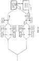
- FIG. 14 is a simplified schematic diagram illustrating a nested modulator system according to another embodiment of the present invention.
- the power measured at node 1405 is utilized to adjust the phase applied to the modulator arm by Phase 3.
- two independent pseudo-random data streams are applied to the two inner MZMs.
- the application of the two independent data streams (which are typically uncorrelated) produces broadband "noise" at the output of the outer MZM when the quadrature bias is not maintained.
- an RMS analog circuit 1410 is used in conjunction with monitor photodiode MPD 3 to detect the power and reduce or minimize the noise generated and to maintain the quadrature bias.
- the "noise” is correlated to the phase error in relation to the desired phase shift of ⁇ /2. Accordingly, a portion of the broadband noise is sampled and reduced or minimized to achieve the desired phase shift.
- MPD 3 can be used to control the bias associated with Phase 3, providing for quadrature on the outer MZM.
- the integrated AC time signal power or the integrated power spectrum is reduced or minimized to control the quadrature bias.
- ⁇ 1 is the relative phase at node 1420 (after the first inner MZM)
- ⁇ 2 is the relative phase at node 1422 (after the second inner MZM)
- ⁇ b is the bias applied by Phase 3 and ⁇ b is the error in the phase
- E is the combined electrical field at 1405 after the inner MZMs coherently combine.
- the power measured at MPD 3 is proportional to:
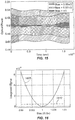
- FIG. 15 is a plot illustrating optical power as a function of time for various biases according to an embodiment of the present invention.
- the optical power associated with the "noise" in the data ranges from about 0.46 to about 0.54 on a normalized power basis (i.e., arbitrary units).
- the optical power decreases to a range of about 0.48 to about 0.52.
- the optical power amplitude fluctuation associated with the noise is negligible.
- reductions in the noise level towards a constant (DC) output power can be used to determine if the bias is at the desired value.
- FIG. 16 is a plot illustrating integrated signal as a function of bias according to an embodiment of the present invention.
- the noise power (i.e., the integrated signal over a 1GHz bandwidth) 1605 is plotted as a function of bias normalized to ⁇ /2.
- some embodiments utilize an RF signal with a wide bandwidth (e.g., 30 GHz), a portion of the wide band noise (e.g., 1 GHz) can be used according to an embodiment of the present invention.
- a "noise" power bandwidth of 1 GHz is utilized in FIGS. 15 and 16 , this is not required by the present invention and other bandwidths can be utilized.
- Curve 1610 in FIG. 16 represents the noise level resulting from other system elements, providing a floor for minimization.
- embodiments of the present invention can reduce the noise associated with the phase error to less than the noise floor from other system elements.
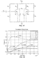
- FIG. 17 is a simplified circuit diagram for a power detector according to an embodiment of the present invention.
- the exemplary RMS circuit illustrated in FIG. 17 can receive the filtered noise signal.
- the output indicates the power present in the filtered noise band.
- FIG. 18 is a plot illustrating transient response at the output of the power detector according to an embodiment of the present invention.
- the output voltage is represented by the curves 1810 and 1812, respectively, which are characterized by a small amplitude.
- the output voltage increases as illustrated by curve 1820 ( ⁇ 5%) and curves 1830 (-10%) and 1832 (+10%).
- the transient response demonstrates that fast changes can be accomplished.
- FIG. 19 is a plot illustrating steady state response at the output of the power detector according to an embodiment of the present invention.
- the steady state voltage is about 0.6 V (curve 1930 for -10% and curve 1932 for +10%).
- curve 1930 for -10% and curve 1932 for +10% the voltage drops as shown by curve 1920 at ⁇ 0.13 V for ⁇ 5% and curve 1910 at ⁇ 0 V for ⁇ 1%.
- FIG. 20 is a plot illustrating voltage output for changes in input noise (i.e., abrupt change in the phase bias error) according to an embodiment of the present invention.
- the quadrature error was increased from 5% to 10% at a time of about 17 ⁇ s
- the voltage changed from the steady state value of ⁇ 0.15 V to a new steady state value of ⁇ 0.6 V in a period of ⁇ 10 ⁇ s.
- time constants of external stimuli are typically on the order of milliseconds.
- the response times of microseconds illustrated in FIG. 20 are fully suitable.
- FIG. 21 is a simplified flowchart illustrating a method of operating a BPSK modulator.
- the method includes receiving an RF signal at the BPSK modulator (2110) and splitting the RF signal into a first portion and a second portion that is inverted with respect to the first portion (2112). As illustrated in FIG. 7 , the RF I and Q signals are split into inverted signals and applied to the BPSK modulators.
- the method also includes receiving the first portion at a first arm of the BPSK modulator (2114) and receiving the second portion at a second arm of the BPSK modulator (2116).
- the method further includes applying a first tone to the first arm of the BPSK modulator (2118) and applying a second tone to the second arm of the BPSK modulator. Additionally, the method includes measuring a power associated with an output of the BPSK modulator (2122) and adjusting a phase applied to at least one of the first arm of the BPSK modulator or the second arm of the BPSK modulator in response to the measured power (2124). Adjusting the phase can include increasing the power associated with the output of the BPSK modulator, for example, maximizing the power. In some embodiments, measuring the power associated with the output of the of the BPSK modulator comprises spectrally filtering the output, for example, by performing band pass filtering at a difference frequency of the first tone and the second tone.
- FIG. 21 provides a particular method of operating a BPSK modulator according to an embodiment of the present invention. Other sequences of steps may also be performed according to alternative embodiments. For example, alternative embodiments of the present invention may perform the steps outlined above in a different order. Moreover, the individual steps illustrated in FIG. 21 may include multiple sub-steps that may be performed in various sequences as appropriate to the individual step. Furthermore, additional steps may be added or removed depending on the particular applications. One of ordinary skill in the art would recognize many variations, modifications, and alternatives.
- FIG. 22 is a simplified flowchart illustrating a method of operating a QPSK modulator.
- the method includes receiving an optical signal at a first BPSK modulator (2210) and generating a first modulated signal at an output of the first BPSK modulator (2212).
- the optical signal is a cw signal provided by a laser source.
- the method further includes receiving the optical signal at a second BPSK modulator (2214) and generating a second modulated signal at an output of the second BPSK modulator (2216).
- the method also includes combining the first modulated signal and the second modulated signal at an output of the QPSK modulator (2218) and measuring a power associated with the output of the QPSK modulator (2220).
- measuring the power can include the use of an RMS analog circuit.
- measuring the power can include spectrally filtering the output of the QPSK modulator into one or more spectral bands before passing the filtered signal to detectors, for example, by applying a 1 GHz bandwidth bandpass filter to the output.
- the method includes adjusting a phase applied to the output of the second BPSK modulator in response to the measured power (2222). It should be understood that it is only the phase difference between the two BPSK modulators is of importance. Thus the phase can be adjusted after each one of the BPSK modulators, or on both of them.
- adjusting the phase applied to the output of the second BPSK modulator can include increasing the phase toward a ⁇ /2 bias, resulting in a decrease in power as the integrated signal approaches the minimum at ⁇ /2 bias.
- adjusting the phase applied to the output of the second BPSK modulator can include decreasing the phase toward a ⁇ /2 bias, resulting in a decrease in power.
- the phase adjustment can be accomplished in several ways, including adjusting a temperature of a heater associated with the second BPSK modulator.
- FIG. 22 provides a particular method of operating a QPSK modulator according to an embodiment of the present invention. Other sequences of steps may also be performed according to alternative embodiments. For example, alternative embodiments of the present invention may perform the steps outlined above in a different order. Moreover, the individual steps illustrated in FIG. 22 may include multiple sub-steps that may be performed in various sequences as appropriate to the individual step. Furthermore, additional steps may be added or removed depending on the particular applications. One of ordinary skill in the art would recognize many variations, modifications, and alternatives.
Landscapes
- Engineering & Computer Science (AREA)
- Computer Networks & Wireless Communication (AREA)
- Signal Processing (AREA)
- Physics & Mathematics (AREA)
- Electromagnetism (AREA)
- Optics & Photonics (AREA)
- Optical Modulation, Optical Deflection, Nonlinear Optics, Optical Demodulation, Optical Logic Elements (AREA)
- Optical Communication System (AREA)
- Digital Transmission Methods That Use Modulated Carrier Waves (AREA)
Claims (10)
- Verfahren zum Betreiben eines BPSK-Modulators zur binären Phasenumtastung, wobei das Verfahren umfasst:- Empfangen eines HF-Signals am BPSK-Modulator zur binären Phasenumtastung;- Aufteilen des HF-Signals in einen ersten Teil und einen zweiten Teil, der in Bezug auf den ersten Teil invertiert ist;- Empfangen des ersten Teils an einem ersten Zweig des BPSK-Modulators zur binären Phasenumtastung;- Empfangen des zweiten Teils an einem zweiten Zweig des BPSK-Modulators zur binären Phasenumtastung;- Anwenden eines ersten Tons auf den ersten Zweig des BPSK-Modulators zur binären Phasenumtastung- Anwenden eines zweiten Tons auf den zweiten Zweig des BPSK-Modulators zur binären Phasenumtastung- Messen einer Leistung, die einem Ausgang des BPSK-Modulators zur binären Phasenumtastung zugeordnet ist, wobei das Messen der Leistung, die dem Ausgang des BPSK-Modulators zugeordnet ist, das spektrale Filtern des Ausgangs umfasst; und- Anpassen einer Phase, die auf den ersten Zweig des BPSK-Modulators für binäre Phasenumtastung und/oder den zweiten Zweig des BPSK-Modulators für binäre Phasenumtastung als Reaktion auf die gemessene Leistung angewendet wird.
- Verfahren nach Anspruch 1, wobei das Anpassen der Phase das Erhöhen der Leistung umfasst, die dem Ausgang des BPSK-Modulators mit binärer Phasenumtastung zugeordnet ist.
- Verfahren nach Anspruch 2, wobei das Erhöhen der Leistung das Maximieren der Leistung umfasst.
- Verfahren nach Anspruch 1, wobei das Messen der Leistung, die dem Ausgang des BPSK-Modulators mit binärer Phasenumtastung zugeordnet ist, die Verwendung eines Spitzenwertdetektors (916) umfasst.
- Verfahren nach Anspruch 4, wobei das spektrale Filtern der Ausgabe das Durchführen einer Bandpassfilterung bei einer Differenzfrequenz von dem ersten Ton und dem zweiten Ton umfasst.
- Verschachteltes Mach-Zehnder-Modulatorsystem, welches für die BPSK-Modulation geeignet ist, aufweisend:- einen optischen Eingangsanschluss (705);- einen Optokoppler, der mit der optischen Eingangsanschluss (705) gekoppelt ist und einen ersten Zweig und einen zweiten Zweig aufweist;- einen ersten inneren Mach-Zehnder-Modulator MZM (710), der mit dem ersten Zweig verbunden ist, worin der erste innere Mach-Zehnder-Modulator MZM (710) einen Phasensteuerabschnitt und einen Ausgang umfasst;- einen ersten Pilotton-Generator, der auf den ersten Zweig einen ersten Pilotton aufbringt;- einen zweiten Pilotton-Generator, der auf den zweiten Zweig einen zweiten Pilotton aufbringt;- einen ersten optischen Detektor, der mit dem Ausgang des ersten inneren Mach-Zehnder-Modulators MZM (710) verbunden ist;- eine Rückkopplungsschleife, die den ersten optischen Detektor (230) mit dem Phasensteuerabschnitt verbindet, wobei die Rückkopplungsschleife (130) eine analoge Schaltung umfasst, die auf eine Intensität von Intermodulationsfrequenzen reagiert, die durch den ersten und zweiten Pilotton erzeugt werden;- einen zweiten inneren Mach-Zehnder-Modulator MZM (712), der mit dem zweiten Zweig verbunden ist und einen zweiten Phasensteuerabschnitt und einen Ausgang aufweist;- einen zweiten Optokoppler, der den Ausgang des ersten inneren Mach-Zehnder-Modulators MZM (710) und den Ausgang des zweiten inneren Mach-Zehnder-Modulators MZM (712) empfängt; und- einen Filter zum spektralen Filtern der Ausgabe des ersten inneren MZM oder des zweiten inneren MZM.
- Verschachteltes Mach-Zehnder-Modulator-MZM-System nach Anspruch 6, weiter aufweisend einen dritten Phasensteuerabschnitt, der mit dem Ausgang des ersten inneren Mach-Zehnder-Modulators MZM (170) und/oder des zweiten inneren Mach-Zehnder-Modulators MZM (172) verbunden ist.
- Verschachteltes Mach-Zehnder-Modulator-MZM-System nach Anspruch 7, weiter aufweisend einen dritten optischen Detektor (234), der mit einem Ausgang des zweiten Optokopplers verbunden ist.
- Verschachteltes Mach-Zehnder-Modulator-MZM-System nach Anspruch 8, weiter aufweisend eine zweite Rückkopplungsschleife, die den dritten optischen Detektor (234) mit dem dritten Phasensteuerabschnitt verbindet.
- Verschachteltes Mach-Zehnder-Modulator-MZM-System nach Anspruch 6, weiter aufweisend einen zweiten optischen Detektor (232), der mit dem Ausgang des zweiten inneren Mach-Zehnder-Modulators MZM (712) gekoppelt ist.
Applications Claiming Priority (2)
| Application Number | Priority Date | Filing Date | Title |
|---|---|---|---|
| US201261680103P | 2012-08-06 | 2012-08-06 | |
| PCT/US2013/053606 WO2014025683A2 (en) | 2012-08-06 | 2013-08-05 | Method and system for the monolithic integration of circuits for monitoring and control of rf signals |
Publications (3)
| Publication Number | Publication Date |
|---|---|
| EP2880764A2 EP2880764A2 (de) | 2015-06-10 |
| EP2880764A4 EP2880764A4 (de) | 2016-04-20 |
| EP2880764B1 true EP2880764B1 (de) | 2019-10-23 |
Family
ID=50025563
Family Applications (1)
| Application Number | Title | Priority Date | Filing Date |
|---|---|---|---|
| EP13827857.7A Active EP2880764B1 (de) | 2012-08-06 | 2013-08-05 | Verfahren und system zur monolithischen integration von schaltungen zur überwachung und steuerung von rf-signalen |
Country Status (4)
| Country | Link |
|---|---|
| US (4) | US9300406B2 (de) |
| EP (1) | EP2880764B1 (de) |
| JP (1) | JP6379091B2 (de) |
| WO (1) | WO2014025683A2 (de) |
Families Citing this family (20)
| Publication number | Priority date | Publication date | Assignee | Title |
|---|---|---|---|---|
| EP2880764B1 (de) | 2012-08-06 | 2019-10-23 | Skorpios Technologies, Inc. | Verfahren und system zur monolithischen integration von schaltungen zur überwachung und steuerung von rf-signalen |
| WO2015160660A1 (en) * | 2014-04-15 | 2015-10-22 | Arris Enterprises, Inc. | Smart receivers and transmitters for catv networks |
| US9400354B2 (en) * | 2014-11-06 | 2016-07-26 | Huawei Technologies Co., Ltd. | Waveguide polarization rotator and method of construction thereof |
| JP6620409B2 (ja) * | 2015-03-11 | 2019-12-18 | 富士通株式会社 | 光送信器、光伝送システム、及び光通信制御方法 |
| US9646639B2 (en) | 2015-06-26 | 2017-05-09 | Western Digital (Fremont), Llc | Heat assisted magnetic recording writer having integrated polarization rotation waveguides |
| WO2017145981A1 (ja) * | 2016-02-23 | 2017-08-31 | 日本電信電話株式会社 | 光送信器 |
| JP6627640B2 (ja) * | 2016-05-16 | 2020-01-08 | 富士通株式会社 | 光送信機 |
| US10536221B2 (en) * | 2018-06-14 | 2020-01-14 | Juniper Networks, Inc. | Methods and apparatus for detecting and compensating bandwidth limitation and modulation nonlinearity of a coherent optical transponder |
| WO2020028409A1 (en) * | 2018-07-30 | 2020-02-06 | The Regents Of The University Of California | Transmitter architecture for generating 4n-qam constellation with no digital-to-analog converters (dac) in signal path requirement |
| WO2020103164A1 (zh) * | 2018-11-24 | 2020-05-28 | 华为技术有限公司 | 偏振处理装置、光收发机和光偏振处理的方法 |
| US11239919B2 (en) * | 2018-12-20 | 2022-02-01 | Acacia Communications, Inc. | Side channel communication for an optical coherent transceiver |
| US10790910B2 (en) * | 2018-12-22 | 2020-09-29 | Intel Corporation | Optical modulator-based transmission control |
| KR20200126647A (ko) * | 2019-04-30 | 2020-11-09 | 삼성전기주식회사 | 프론트 엔드 모듈 |
| JP7323042B2 (ja) * | 2020-02-20 | 2023-08-08 | 日本電信電話株式会社 | 光iq変調器 |
| DE102020207050A1 (de) * | 2020-06-05 | 2021-12-09 | Universität Paderborn | Elektrooptischer Regelkreis |
| US11005572B1 (en) * | 2020-11-09 | 2021-05-11 | Xilinx, Inc. | Temperature-locked loop for optical elements having a temperature-dependent response |
| WO2022137517A1 (en) * | 2020-12-25 | 2022-06-30 | Nec Corporation | Optical transmitter and method of transmitting an optical signal |
| WO2023084708A1 (ja) * | 2021-11-11 | 2023-05-19 | 日本電気株式会社 | 光変調器及び光変調方法 |
| CN114866154B (zh) * | 2022-03-25 | 2023-05-12 | 中国电子科技集团公司第二十九研究所 | 超宽带射频信号高速bpsk相位调制装置及方法 |
| US20240348343A1 (en) * | 2023-04-11 | 2024-10-17 | Phase Sensitive Innovations, Inc. | Polarization-Diverse Radio Receive Element, Receiver, Transceiver and Related Methods of Operation |
Citations (3)
| Publication number | Priority date | Publication date | Assignee | Title |
|---|---|---|---|---|
| US20050117191A1 (en) * | 2001-11-30 | 2005-06-02 | Robert Griffin | Modulation control |
| US20060034616A1 (en) * | 2004-08-13 | 2006-02-16 | Alan Tipper | Automatic bias control for an optical modulator |
| WO2011104838A1 (ja) * | 2010-02-25 | 2011-09-01 | 三菱電機株式会社 | 光送信器 |
Family Cites Families (82)
| Publication number | Priority date | Publication date | Assignee | Title |
|---|---|---|---|---|
| US3434056A (en) * | 1966-05-31 | 1969-03-18 | Bell Telephone Labor Inc | Distortion monitoring by comparing square and cubic law distortion to carrier |
| US4777459A (en) | 1987-06-08 | 1988-10-11 | Hughes Aircraft Company | Microwave multiplexer with multimode filter |
| US5106764A (en) | 1989-04-10 | 1992-04-21 | At&T Bell Laboratories | Device fabrication |
| US5077728A (en) | 1989-12-20 | 1991-12-31 | At&T Bell Laboratories | Frequency division multiple access network |
| US5077816A (en) | 1989-12-26 | 1991-12-31 | United Technologies Corporation | Fiber embedded grating frequency standard optical communication devices |
| US5659413A (en) | 1995-02-28 | 1997-08-19 | The Mitre Corporation | Laser satellite communication system |
| JPH11513138A (ja) | 1996-07-02 | 1999-11-09 | コーニング インコーポレイテッド | 偏光感度を低減した回折格子 |
| DE19746350A1 (de) | 1997-10-21 | 1999-04-22 | Bosch Gmbh Robert | Transceiver für Wellenlängemultiplex-Verfahren |
| US20020181067A1 (en) | 1997-10-29 | 2002-12-05 | Romanovsky Alexander B. | Electro-optic switching assembly and method |
| US6101026A (en) | 1998-01-27 | 2000-08-08 | Agilent Technologies, Inc. | Reversible amplifier for optical networks |
| GB2370473B (en) | 2000-12-21 | 2004-04-07 | Marconi Caswell Ltd | Improvements in or relating to optical communication |
| US20020110328A1 (en) | 2001-02-14 | 2002-08-15 | Bischel William K. | Multi-channel laser pump source for optical amplifiers |
| US7203429B2 (en) | 2001-05-07 | 2007-04-10 | Tyco Telecommunications (Us) Inc. | Optical transmission system using optical signal processing in terminals for improved system performance |
| US20030198470A1 (en) | 2002-04-23 | 2003-10-23 | Richard Lauder | WDM assembly |
| US7173991B2 (en) | 2002-06-17 | 2007-02-06 | Hitachi, Ltd. | Methods and apparatus for spectral filtering channel estimates |
| US7149424B2 (en) * | 2002-08-22 | 2006-12-12 | Siemens Communications, Inc. | Method and device for evaluating and improving the quality of transmission of a telecommunications signal through an optical fiber |
| JP4502323B2 (ja) | 2002-09-25 | 2010-07-14 | ホーヤ コーポレイション ユーエスエイ | 光学装置 |
| AU2003284380A1 (en) | 2002-10-30 | 2004-06-07 | Matteo Cherchi | An integrated optic polarization converter based on structural chirality |
| JP4789619B2 (ja) | 2002-11-12 | 2011-10-12 | ホーヤ コーポレイション ユーエスエイ | 光学装置および光学装置を組み込んだ光学アセンブリ |
| US7085453B2 (en) | 2002-11-25 | 2006-08-01 | Matsushita Electric Industrial Co., Ltd. | Optical functional device and optical module |
| US7209664B1 (en) | 2003-06-10 | 2007-04-24 | Nortel Networks Limited | Frequency agile transmitter and receiver architecture for DWDM systems |
| US8050351B2 (en) * | 2003-07-02 | 2011-11-01 | Celight, Inc. | Quadrature modulator with feedback control and optical communications system using the same |
| US7099586B2 (en) | 2003-09-04 | 2006-08-29 | The Regents Of The University Of California | Reconfigurable multi-channel all-optical regenerators |
| DE112004000077B4 (de) | 2003-10-06 | 2012-01-19 | Murata Manufacturing Co., Ltd. | Verdrillter Wellenleiter und drahtlose Vorrichtung |
| US7209612B2 (en) | 2004-03-24 | 2007-04-24 | Enablence Inc. | Two-stage optical bi-directional transceiver |
| US20060002443A1 (en) | 2004-06-30 | 2006-01-05 | Gennady Farber | Multimode external cavity semiconductor lasers |
| KR100617709B1 (ko) * | 2004-08-05 | 2006-08-28 | 삼성전자주식회사 | 주파수 변조 방식의 광송신 장치 및 방법 |
| WO2006045324A1 (en) | 2004-10-22 | 2006-05-04 | Pirelli & C. S.P.A. | Method and device for stabilizing the state of polarization of a polarization multiplexed optical radiation |
| US20060153566A1 (en) | 2005-01-13 | 2006-07-13 | Sorin Wayne V | Methods and apparatuses to provide a wavelength-division-multiplexing passive optical network with asymmetric data rates |
| JP4922594B2 (ja) * | 2005-05-23 | 2012-04-25 | 富士通株式会社 | 光送信装置、光受信装置、およびそれらを含む光通信システム |
| US7702188B2 (en) | 2005-09-08 | 2010-04-20 | Infinera Corporation | Polarization beam splitter-polarization rotator structure |
| JP4884750B2 (ja) * | 2005-11-10 | 2012-02-29 | 三菱電機株式会社 | 光変調器およびそのバイアス制御方法 |
| US7603153B2 (en) | 2005-12-12 | 2009-10-13 | Sterling Investments Lc | Multi-element probe array |
| EP2003486A4 (de) * | 2006-03-31 | 2010-11-24 | Fujitsu Ltd | Differenz-vierphasen-verschiebungs-modulator und verfahren zum steuern des phasenverschiebungsbetrags dafür |
| US7298935B1 (en) | 2006-05-01 | 2007-11-20 | International Business Machines Corporation | Waveguide polarization beam splitters and method of fabricating a waveguide wire-grid polarization beam splitter |
| US7317874B2 (en) | 2006-06-02 | 2008-01-08 | Broadway Networks, Inc. | Adaptive optical transceiver for fiber access communications |
| US7821712B2 (en) | 2006-06-29 | 2010-10-26 | Accelink Technologies Co., Ltd. | Thin film tunable optical filter |
| WO2008066159A1 (fr) | 2006-12-01 | 2008-06-05 | Nec Corporation | Rotateur de polarisation et procédé de fabrication afférent |
| US8150219B2 (en) | 2007-01-10 | 2012-04-03 | Nippon Telegraph And Telephone Corporation | Waveguide-type optical interferometer |
| JP2008187223A (ja) | 2007-01-26 | 2008-08-14 | Hitachi Communication Technologies Ltd | 光位相変調器の制御法 |
| US8655114B2 (en) | 2007-03-26 | 2014-02-18 | Massachusetts Institute Of Technology | Hitless tuning and switching of optical resonator amplitude and phase responses |
| JP2008244767A (ja) | 2007-03-27 | 2008-10-09 | Nec Corp | 光受信装置および光送受信装置 |
| US20090010648A1 (en) | 2007-07-02 | 2009-01-08 | Tellabs Bedford, Inc. | Methods and apparatus for upgrading passive optical networks |
| US20090047019A1 (en) | 2007-08-13 | 2009-02-19 | Paparao Palacharla | Method and System for Communicating Optical Traffic |
| US7565041B2 (en) | 2007-10-26 | 2009-07-21 | Infinera Corporation | Symmetric optical circuit with integrated polarization rotator |
| WO2009059144A1 (en) | 2007-11-01 | 2009-05-07 | Massachusetts Institute Of Technology | Magnetic material for magneto-optical isolator |
| US7701985B2 (en) | 2007-11-09 | 2010-04-20 | Lightwire, Inc. | SOI-based tunable laser |
| US8180216B2 (en) * | 2007-12-20 | 2012-05-15 | Verizon Patent And Licensing Inc. | Latency measurement in optical networks |
| WO2010016295A1 (ja) | 2008-08-06 | 2010-02-11 | 日本電気株式会社 | 波長可変光送信機 |
| US8126329B2 (en) | 2008-09-03 | 2012-02-28 | Applied Optoelectronics, Inc. | Quad-port optical module with pass-through and add/drop configuration |
| US20100129077A1 (en) | 2008-11-24 | 2010-05-27 | Nortel Networks Limited | Techniques for implementing a dual array waveguide filter for a wavelength division multiplexed passive optical network |
| US20100142964A1 (en) * | 2008-12-08 | 2010-06-10 | Sun-Hyok Chang | Optical transmission apparatus with stable optical signal output |
| WO2010075886A1 (en) | 2008-12-30 | 2010-07-08 | Nokia Siemens Networks Oy | Method and arrangement for transmitting signals in a point to multipoint network |
| US8849072B2 (en) | 2009-02-13 | 2014-09-30 | Physical Sciences, Inc. | Surface plasmon enhanced optical devices for integrated photonics |
| EP2247004B1 (de) * | 2009-04-28 | 2015-06-03 | Alcatel Lucent | Verfahren zur Datenübertragung unter Verwendung eines LINC-Verstärkers, LINC-Verstärker, Übertragungsvorrichtung, Empfangsvorrichtung und Kommunikationsnetz dafür |
| US8655115B2 (en) | 2009-05-25 | 2014-02-18 | Pusan National University Industry-University Cooperation Foundation | Integrated polymer optical waveguide current sensor |
| US8655181B2 (en) | 2009-06-01 | 2014-02-18 | Mitsubishi Electric Corporation | Optical transmission/reception module |
| TWI466466B (zh) | 2009-06-12 | 2014-12-21 | Univ Nat Taiwan Science Tech | 具雙向性之多波長路由與放大模組 |
| WO2011032597A1 (en) | 2009-09-18 | 2011-03-24 | Telefonaktiebolaget Lm Ericsson (Publ) | Passive optical network |
| JP2011077133A (ja) | 2009-09-29 | 2011-04-14 | Oki Electric Industry Co Ltd | 光双方向通信モジュール及び光双方向通信装置 |
| US8615025B2 (en) | 2009-10-13 | 2013-12-24 | Skorpios Technologies, Inc. | Method and system for hybrid integration of a tunable laser |
| JP5375519B2 (ja) * | 2009-10-26 | 2013-12-25 | 富士通株式会社 | 非線形歪検出回路、光受信機、光伝送システム、および非線形歪検出方法 |
| US8897606B2 (en) | 2009-12-15 | 2014-11-25 | Kotura, Inc. | Ring resonator with wavelength selectivity |
| US8160405B2 (en) | 2009-12-23 | 2012-04-17 | Infinera Corporation | Optical integrated circuit |
| US8548333B2 (en) | 2010-04-02 | 2013-10-01 | Infinera Corporation | Transceiver photonic integrated circuit |
| US8634718B2 (en) | 2010-05-28 | 2014-01-21 | Infinera Corporation | Polarization control in a photonic integrated circuit |
| EP2586146A4 (de) | 2010-06-22 | 2016-11-23 | Technion R&D Foundation | Optische netzwerkeinheit, optisches zugangsnetzwerk und verfahren zum austausch von informationen |
| EP2630738B1 (de) | 2010-12-03 | 2016-02-24 | Huawei Technologies Co., Ltd. | Farblose und dichte wellenlängenteilungs-multiplexing-sender |
| US8222084B2 (en) | 2010-12-08 | 2012-07-17 | Skorpios Technologies, Inc. | Method and system for template assisted wafer bonding |
| JP5853386B2 (ja) * | 2010-12-16 | 2016-02-09 | 富士通オプティカルコンポーネンツ株式会社 | 光変調装置および光変調制御方法 |
| CN103492537A (zh) | 2011-04-22 | 2014-01-01 | 格雷特波因特能源公司 | 伴随焦炭选矿的碳质原料加氢甲烷化 |
| EP2518912B1 (de) | 2011-04-29 | 2014-12-24 | ADVA Optical Networking SE | Abschlussknoten einer optischen Leitung und passives optisches Netzwerk |
| EP2525517B1 (de) | 2011-05-20 | 2016-05-04 | ADVA Optical Networking SE | Optisches Wellenlängenmultiplex-Übertragungssystem, besonders ein passives optisches Wellenlängenmultiplexnetzwerk |
| JP5874202B2 (ja) * | 2011-05-30 | 2016-03-02 | 富士通株式会社 | 光送信装置、その制御方法、及び光伝送システム |
| US9091813B2 (en) | 2011-06-08 | 2015-07-28 | Skorpios Technologies, Inc. | Systems and methods for photonic polarization beam splitters |
| US9031408B2 (en) | 2011-06-09 | 2015-05-12 | Telefonaktiebolaget L M Ericsson (Publ) | Method for fast wavelength division multiplexing (WDM) passive optical network (PON) initialization in heterogeneous networks |
| EP2573966B1 (de) | 2011-07-20 | 2013-11-13 | ADVA Optical Networking SE | Wellenlängenkopplungsverfahren für eine optische Sende-/Empfangsvorrichtung und optische Sende-/Empfangsvorrichtung |
| US8320760B1 (en) | 2011-11-03 | 2012-11-27 | Google Inc. | Passive optical network with asymmetric modulation scheme |
| US9287984B2 (en) | 2011-12-21 | 2016-03-15 | Skorpios Technologies, Inc. | Tunable bi-directional transceiver |
| KR20130085763A (ko) | 2012-01-20 | 2013-07-30 | 삼성전자주식회사 | 광 집적 회로용 혼성 레이저 광원 |
| US9337933B2 (en) | 2012-10-19 | 2016-05-10 | Skorpios Technologies, Inc. | Integrated optical network unit |
| EP2880764B1 (de) | 2012-08-06 | 2019-10-23 | Skorpios Technologies, Inc. | Verfahren und system zur monolithischen integration von schaltungen zur überwachung und steuerung von rf-signalen |
-
2013
- 2013-08-05 EP EP13827857.7A patent/EP2880764B1/de active Active
- 2013-08-05 US US13/959,107 patent/US9300406B2/en active Active
- 2013-08-05 JP JP2015526604A patent/JP6379091B2/ja active Active
- 2013-08-05 WO PCT/US2013/053606 patent/WO2014025683A2/en not_active Ceased
-
2016
- 2016-02-19 US US15/048,222 patent/US9479262B2/en active Active
- 2016-09-23 US US15/274,714 patent/US9960854B2/en active Active
-
2018
- 2018-04-06 US US15/947,555 patent/US10200131B2/en active Active
Patent Citations (3)
| Publication number | Priority date | Publication date | Assignee | Title |
|---|---|---|---|---|
| US20050117191A1 (en) * | 2001-11-30 | 2005-06-02 | Robert Griffin | Modulation control |
| US20060034616A1 (en) * | 2004-08-13 | 2006-02-16 | Alan Tipper | Automatic bias control for an optical modulator |
| WO2011104838A1 (ja) * | 2010-02-25 | 2011-09-01 | 三菱電機株式会社 | 光送信器 |
Also Published As
| Publication number | Publication date |
|---|---|
| US20140037286A1 (en) | 2014-02-06 |
| US9960854B2 (en) | 2018-05-01 |
| WO2014025683A3 (en) | 2015-04-09 |
| JP2015530612A (ja) | 2015-10-15 |
| JP6379091B2 (ja) | 2018-08-22 |
| US10200131B2 (en) | 2019-02-05 |
| US20160248516A1 (en) | 2016-08-25 |
| US9300406B2 (en) | 2016-03-29 |
| US9479262B2 (en) | 2016-10-25 |
| US20180331765A1 (en) | 2018-11-15 |
| US20170201325A1 (en) | 2017-07-13 |
| EP2880764A4 (de) | 2016-04-20 |
| WO2014025683A2 (en) | 2014-02-13 |
| EP2880764A2 (de) | 2015-06-10 |
Similar Documents
| Publication | Publication Date | Title |
|---|---|---|
| EP2880764B1 (de) | Verfahren und system zur monolithischen integration von schaltungen zur überwachung und steuerung von rf-signalen | |
| JP5405716B2 (ja) | 光送信機 | |
| EP2107418B1 (de) | Optisches qam-system umfassend einen optischen modulator und eine regelungsvorrichtung und verfahren zur steuerung des optischen modulators | |
| EP2267923B1 (de) | Optisches Übertragungssystem | |
| JP5712935B2 (ja) | 波長分散を検出する方法及び装置並びに波長分散を補償する方法及び装置 | |
| EP2042913A2 (de) | Optischer Modulator beruhend auf einer Quadratur-Phasenumtastung | |
| US20100021182A1 (en) | Optical transmitter | |
| US9614639B2 (en) | Power control of optical signals having different polarizations | |
| JP2007043638A (ja) | 光送信装置、光受信装置、およびそれらを含む光通信システム | |
| EP2778771B1 (de) | Trägerunterdrückte lichterzeugende vorrichtung | |
| WO2003067768A2 (en) | Pulse generation for optical communications | |
| JP2019506037A (ja) | InPベースの光送信機における光学的障害の特性評価および補償 | |
| US10234704B2 (en) | Optical module that includes optical modulator and bias control method for optical modulator | |
| US6674936B2 (en) | Polarization mode dispersion compensation using a wavelength locked loop | |
| JP3937237B2 (ja) | 光周波数シフトキーイング変調器 | |
| Baier et al. | 112 Gb/s PDM-PAM4 generation and 80 km transmission using a novel monolithically integrated dual-polarization electro-absorption modulator InP PIC | |
| US10425166B2 (en) | Optical transmitter, optical transmission apparatus, and optical modulation method | |
| Rausch et al. | A performance comparison of single-ended-and differential driving scheme at 64 Gbit/s QPSK modulation for InP-based IQ-Mach-Zehnder modulators in serial-push-pull configuration | |
| JP2001244896A (ja) | 光送信装置 | |
| JP2009080189A (ja) | 光変調装置 | |
| US8139952B2 (en) | System and method for measuring the extinction ratio of an optical transmitter using an interferogram wing-to-peak ratio | |
| Huang et al. | Instantaneous Frequency Measurement using Single Sideband Modulation of Mach-Zehnder Modulators | |
| Zhang et al. | Microwave frequency measurement using photonic methods |
Legal Events
| Date | Code | Title | Description |
|---|---|---|---|
| PUAI | Public reference made under article 153(3) epc to a published international application that has entered the european phase |
Free format text: ORIGINAL CODE: 0009012 |
|
| 17P | Request for examination filed |
Effective date: 20150304 |
|
| AK | Designated contracting states |
Kind code of ref document: A2 Designated state(s): AL AT BE BG CH CY CZ DE DK EE ES FI FR GB GR HR HU IE IS IT LI LT LU LV MC MK MT NL NO PL PT RO RS SE SI SK SM TR |
|
| AX | Request for extension of the european patent |
Extension state: BA ME |
|
| REG | Reference to a national code |
Ref country code: DE Ref legal event code: R079 Free format text: PREVIOUS MAIN CLASS: H99Z9999999999 Ipc: H04B0010000000 Ref country code: DE Ref legal event code: R079 Ref document number: 602013062081 Country of ref document: DE Free format text: PREVIOUS MAIN CLASS: H99Z9999999999 Ipc: H04B0010000000 |
|
| DAX | Request for extension of the european patent (deleted) | ||
| A4 | Supplementary search report drawn up and despatched |
Effective date: 20160318 |
|
| RIC1 | Information provided on ipc code assigned before grant |
Ipc: H04B 10/50 20130101AFI20160314BHEP Ipc: H04B 10/556 20130101ALI20160314BHEP |
|
| RAP1 | Party data changed (applicant data changed or rights of an application transferred) |
Owner name: SKORPIOS TECHNOLOGIES, INC. |
|
| STAA | Information on the status of an ep patent application or granted ep patent |
Free format text: STATUS: EXAMINATION IS IN PROGRESS |
|
| 17Q | First examination report despatched |
Effective date: 20180605 |
|
| REG | Reference to a national code |
Ref country code: DE Ref legal event code: R079 Ref document number: 602013062081 Country of ref document: DE Free format text: PREVIOUS MAIN CLASS: H04B0010000000 Ipc: H04L0027200000 |
|
| RIC1 | Information provided on ipc code assigned before grant |
Ipc: H04L 27/20 20060101AFI20190320BHEP Ipc: H04B 10/50 20130101ALI20190320BHEP Ipc: H04J 14/02 20060101ALI20190320BHEP Ipc: H04B 10/079 20130101ALI20190320BHEP Ipc: H04B 10/564 20130101ALI20190320BHEP Ipc: H04B 10/556 20130101ALI20190320BHEP |
|
| GRAP | Despatch of communication of intention to grant a patent |
Free format text: ORIGINAL CODE: EPIDOSNIGR1 |
|
| STAA | Information on the status of an ep patent application or granted ep patent |
Free format text: STATUS: GRANT OF PATENT IS INTENDED |
|
| INTG | Intention to grant announced |
Effective date: 20190502 |
|
| GRAS | Grant fee paid |
Free format text: ORIGINAL CODE: EPIDOSNIGR3 |
|
| GRAA | (expected) grant |
Free format text: ORIGINAL CODE: 0009210 |
|
| STAA | Information on the status of an ep patent application or granted ep patent |
Free format text: STATUS: THE PATENT HAS BEEN GRANTED |
|
| AK | Designated contracting states |
Kind code of ref document: B1 Designated state(s): AL AT BE BG CH CY CZ DE DK EE ES FI FR GB GR HR HU IE IS IT LI LT LU LV MC MK MT NL NO PL PT RO RS SE SI SK SM TR |
|
| REG | Reference to a national code |
Ref country code: GB Ref legal event code: FG4D |
|
| REG | Reference to a national code |
Ref country code: CH Ref legal event code: EP |
|
| REG | Reference to a national code |
Ref country code: IE Ref legal event code: FG4D |
|
| REG | Reference to a national code |
Ref country code: DE Ref legal event code: R096 Ref document number: 602013062081 Country of ref document: DE |
|
| REG | Reference to a national code |
Ref country code: AT Ref legal event code: REF Ref document number: 1194941 Country of ref document: AT Kind code of ref document: T Effective date: 20191115 |
|
| REG | Reference to a national code |
Ref country code: NL Ref legal event code: MP Effective date: 20191023 |
|
| REG | Reference to a national code |
Ref country code: LT Ref legal event code: MG4D |
|
| PG25 | Lapsed in a contracting state [announced via postgrant information from national office to epo] |
Ref country code: ES Free format text: LAPSE BECAUSE OF FAILURE TO SUBMIT A TRANSLATION OF THE DESCRIPTION OR TO PAY THE FEE WITHIN THE PRESCRIBED TIME-LIMIT Effective date: 20191023 Ref country code: LT Free format text: LAPSE BECAUSE OF FAILURE TO SUBMIT A TRANSLATION OF THE DESCRIPTION OR TO PAY THE FEE WITHIN THE PRESCRIBED TIME-LIMIT Effective date: 20191023 Ref country code: NL Free format text: LAPSE BECAUSE OF FAILURE TO SUBMIT A TRANSLATION OF THE DESCRIPTION OR TO PAY THE FEE WITHIN THE PRESCRIBED TIME-LIMIT Effective date: 20191023 Ref country code: NO Free format text: LAPSE BECAUSE OF FAILURE TO SUBMIT A TRANSLATION OF THE DESCRIPTION OR TO PAY THE FEE WITHIN THE PRESCRIBED TIME-LIMIT Effective date: 20200123 Ref country code: PL Free format text: LAPSE BECAUSE OF FAILURE TO SUBMIT A TRANSLATION OF THE DESCRIPTION OR TO PAY THE FEE WITHIN THE PRESCRIBED TIME-LIMIT Effective date: 20191023 Ref country code: GR Free format text: LAPSE BECAUSE OF FAILURE TO SUBMIT A TRANSLATION OF THE DESCRIPTION OR TO PAY THE FEE WITHIN THE PRESCRIBED TIME-LIMIT Effective date: 20200124 Ref country code: FI Free format text: LAPSE BECAUSE OF FAILURE TO SUBMIT A TRANSLATION OF THE DESCRIPTION OR TO PAY THE FEE WITHIN THE PRESCRIBED TIME-LIMIT Effective date: 20191023 Ref country code: BG Free format text: LAPSE BECAUSE OF FAILURE TO SUBMIT A TRANSLATION OF THE DESCRIPTION OR TO PAY THE FEE WITHIN THE PRESCRIBED TIME-LIMIT Effective date: 20200123 Ref country code: PT Free format text: LAPSE BECAUSE OF FAILURE TO SUBMIT A TRANSLATION OF THE DESCRIPTION OR TO PAY THE FEE WITHIN THE PRESCRIBED TIME-LIMIT Effective date: 20200224 Ref country code: LV Free format text: LAPSE BECAUSE OF FAILURE TO SUBMIT A TRANSLATION OF THE DESCRIPTION OR TO PAY THE FEE WITHIN THE PRESCRIBED TIME-LIMIT Effective date: 20191023 Ref country code: SE Free format text: LAPSE BECAUSE OF FAILURE TO SUBMIT A TRANSLATION OF THE DESCRIPTION OR TO PAY THE FEE WITHIN THE PRESCRIBED TIME-LIMIT Effective date: 20191023 |
|
| PG25 | Lapsed in a contracting state [announced via postgrant information from national office to epo] |
Ref country code: RS Free format text: LAPSE BECAUSE OF FAILURE TO SUBMIT A TRANSLATION OF THE DESCRIPTION OR TO PAY THE FEE WITHIN THE PRESCRIBED TIME-LIMIT Effective date: 20191023 Ref country code: IS Free format text: LAPSE BECAUSE OF FAILURE TO SUBMIT A TRANSLATION OF THE DESCRIPTION OR TO PAY THE FEE WITHIN THE PRESCRIBED TIME-LIMIT Effective date: 20200224 Ref country code: HR Free format text: LAPSE BECAUSE OF FAILURE TO SUBMIT A TRANSLATION OF THE DESCRIPTION OR TO PAY THE FEE WITHIN THE PRESCRIBED TIME-LIMIT Effective date: 20191023 |
|
| PG25 | Lapsed in a contracting state [announced via postgrant information from national office to epo] |
Ref country code: AL Free format text: LAPSE BECAUSE OF FAILURE TO SUBMIT A TRANSLATION OF THE DESCRIPTION OR TO PAY THE FEE WITHIN THE PRESCRIBED TIME-LIMIT Effective date: 20191023 |
|
| REG | Reference to a national code |
Ref country code: DE Ref legal event code: R097 Ref document number: 602013062081 Country of ref document: DE |
|
| PG2D | Information on lapse in contracting state deleted |
Ref country code: IS |
|
| PG25 | Lapsed in a contracting state [announced via postgrant information from national office to epo] |
Ref country code: IS Free format text: LAPSE BECAUSE OF FAILURE TO SUBMIT A TRANSLATION OF THE DESCRIPTION OR TO PAY THE FEE WITHIN THE PRESCRIBED TIME-LIMIT Effective date: 20200223 Ref country code: DK Free format text: LAPSE BECAUSE OF FAILURE TO SUBMIT A TRANSLATION OF THE DESCRIPTION OR TO PAY THE FEE WITHIN THE PRESCRIBED TIME-LIMIT Effective date: 20191023 Ref country code: RO Free format text: LAPSE BECAUSE OF FAILURE TO SUBMIT A TRANSLATION OF THE DESCRIPTION OR TO PAY THE FEE WITHIN THE PRESCRIBED TIME-LIMIT Effective date: 20191023 Ref country code: EE Free format text: LAPSE BECAUSE OF FAILURE TO SUBMIT A TRANSLATION OF THE DESCRIPTION OR TO PAY THE FEE WITHIN THE PRESCRIBED TIME-LIMIT Effective date: 20191023 Ref country code: CZ Free format text: LAPSE BECAUSE OF FAILURE TO SUBMIT A TRANSLATION OF THE DESCRIPTION OR TO PAY THE FEE WITHIN THE PRESCRIBED TIME-LIMIT Effective date: 20191023 |
|
| REG | Reference to a national code |
Ref country code: AT Ref legal event code: MK05 Ref document number: 1194941 Country of ref document: AT Kind code of ref document: T Effective date: 20191023 |
|
| PLBE | No opposition filed within time limit |
Free format text: ORIGINAL CODE: 0009261 |
|
| STAA | Information on the status of an ep patent application or granted ep patent |
Free format text: STATUS: NO OPPOSITION FILED WITHIN TIME LIMIT |
|
| PG25 | Lapsed in a contracting state [announced via postgrant information from national office to epo] |
Ref country code: SK Free format text: LAPSE BECAUSE OF FAILURE TO SUBMIT A TRANSLATION OF THE DESCRIPTION OR TO PAY THE FEE WITHIN THE PRESCRIBED TIME-LIMIT Effective date: 20191023 Ref country code: IT Free format text: LAPSE BECAUSE OF FAILURE TO SUBMIT A TRANSLATION OF THE DESCRIPTION OR TO PAY THE FEE WITHIN THE PRESCRIBED TIME-LIMIT Effective date: 20191023 Ref country code: SM Free format text: LAPSE BECAUSE OF FAILURE TO SUBMIT A TRANSLATION OF THE DESCRIPTION OR TO PAY THE FEE WITHIN THE PRESCRIBED TIME-LIMIT Effective date: 20191023 |
|
| 26N | No opposition filed |
Effective date: 20200724 |
|
| PG25 | Lapsed in a contracting state [announced via postgrant information from national office to epo] |
Ref country code: AT Free format text: LAPSE BECAUSE OF FAILURE TO SUBMIT A TRANSLATION OF THE DESCRIPTION OR TO PAY THE FEE WITHIN THE PRESCRIBED TIME-LIMIT Effective date: 20191023 Ref country code: SI Free format text: LAPSE BECAUSE OF FAILURE TO SUBMIT A TRANSLATION OF THE DESCRIPTION OR TO PAY THE FEE WITHIN THE PRESCRIBED TIME-LIMIT Effective date: 20191023 |
|
| PG25 | Lapsed in a contracting state [announced via postgrant information from national office to epo] |
Ref country code: MC Free format text: LAPSE BECAUSE OF FAILURE TO SUBMIT A TRANSLATION OF THE DESCRIPTION OR TO PAY THE FEE WITHIN THE PRESCRIBED TIME-LIMIT Effective date: 20191023 |
|
| REG | Reference to a national code |
Ref country code: CH Ref legal event code: PL |
|
| GBPC | Gb: european patent ceased through non-payment of renewal fee |
Effective date: 20200805 |
|
| PG25 | Lapsed in a contracting state [announced via postgrant information from national office to epo] |
Ref country code: CH Free format text: LAPSE BECAUSE OF NON-PAYMENT OF DUE FEES Effective date: 20200831 Ref country code: LI Free format text: LAPSE BECAUSE OF NON-PAYMENT OF DUE FEES Effective date: 20200831 Ref country code: LU Free format text: LAPSE BECAUSE OF NON-PAYMENT OF DUE FEES Effective date: 20200805 |
|
| REG | Reference to a national code |
Ref country code: BE Ref legal event code: MM Effective date: 20200831 |
|
| PG25 | Lapsed in a contracting state [announced via postgrant information from national office to epo] |
Ref country code: FR Free format text: LAPSE BECAUSE OF NON-PAYMENT OF DUE FEES Effective date: 20200831 |
|
| PG25 | Lapsed in a contracting state [announced via postgrant information from national office to epo] |
Ref country code: BE Free format text: LAPSE BECAUSE OF NON-PAYMENT OF DUE FEES Effective date: 20200831 Ref country code: IE Free format text: LAPSE BECAUSE OF NON-PAYMENT OF DUE FEES Effective date: 20200805 Ref country code: GB Free format text: LAPSE BECAUSE OF NON-PAYMENT OF DUE FEES Effective date: 20200805 |
|
| PG25 | Lapsed in a contracting state [announced via postgrant information from national office to epo] |
Ref country code: TR Free format text: LAPSE BECAUSE OF FAILURE TO SUBMIT A TRANSLATION OF THE DESCRIPTION OR TO PAY THE FEE WITHIN THE PRESCRIBED TIME-LIMIT Effective date: 20191023 Ref country code: MT Free format text: LAPSE BECAUSE OF FAILURE TO SUBMIT A TRANSLATION OF THE DESCRIPTION OR TO PAY THE FEE WITHIN THE PRESCRIBED TIME-LIMIT Effective date: 20191023 Ref country code: CY Free format text: LAPSE BECAUSE OF FAILURE TO SUBMIT A TRANSLATION OF THE DESCRIPTION OR TO PAY THE FEE WITHIN THE PRESCRIBED TIME-LIMIT Effective date: 20191023 |
|
| PG25 | Lapsed in a contracting state [announced via postgrant information from national office to epo] |
Ref country code: MK Free format text: LAPSE BECAUSE OF FAILURE TO SUBMIT A TRANSLATION OF THE DESCRIPTION OR TO PAY THE FEE WITHIN THE PRESCRIBED TIME-LIMIT Effective date: 20191023 |
|
| P01 | Opt-out of the competence of the unified patent court (upc) registered |
Effective date: 20230517 |
|
| PGFP | Annual fee paid to national office [announced via postgrant information from national office to epo] |
Ref country code: DE Payment date: 20250611 Year of fee payment: 13 |