EP2882098A1 - Amplifier and radiation detector - Google Patents
Amplifier and radiation detector Download PDFInfo
- Publication number
- EP2882098A1 EP2882098A1 EP13825254.9A EP13825254A EP2882098A1 EP 2882098 A1 EP2882098 A1 EP 2882098A1 EP 13825254 A EP13825254 A EP 13825254A EP 2882098 A1 EP2882098 A1 EP 2882098A1
- Authority
- EP
- European Patent Office
- Prior art keywords
- bonding pad
- interconnection layer
- amplifying circuit
- preamplifier
- layer
- Prior art date
- Legal status (The legal status is an assumption and is not a legal conclusion. Google has not performed a legal analysis and makes no representation as to the accuracy of the status listed.)
- Granted
Links
Images





Classifications
-
- H—ELECTRICITY
- H03—ELECTRONIC CIRCUITRY
- H03F—AMPLIFIERS
- H03F1/00—Details of amplifiers with only discharge tubes, only semiconductor devices or only unspecified devices as amplifying elements
- H03F1/26—Modifications of amplifiers to reduce influence of noise generated by amplifying elements
-
- G—PHYSICS
- G01—MEASURING; TESTING
- G01T—MEASUREMENT OF NUCLEAR OR X-RADIATION
- G01T1/00—Measuring X-radiation, gamma radiation, corpuscular radiation, or cosmic radiation
- G01T1/16—Measuring radiation intensity
- G01T1/17—Circuit arrangements not adapted to a particular type of detector
-
- G—PHYSICS
- G01—MEASURING; TESTING
- G01T—MEASUREMENT OF NUCLEAR OR X-RADIATION
- G01T1/00—Measuring X-radiation, gamma radiation, corpuscular radiation, or cosmic radiation
- G01T1/16—Measuring radiation intensity
- G01T1/24—Measuring radiation intensity with semiconductor detectors
-
- H—ELECTRICITY
- H03—ELECTRONIC CIRCUITRY
- H03F—AMPLIFIERS
- H03F3/00—Amplifiers with only discharge tubes or only semiconductor devices as amplifying elements
- H03F3/04—Amplifiers with only discharge tubes or only semiconductor devices as amplifying elements with semiconductor devices only
- H03F3/08—Amplifiers with only discharge tubes or only semiconductor devices as amplifying elements with semiconductor devices only controlled by light
-
- H—ELECTRICITY
- H03—ELECTRONIC CIRCUITRY
- H03F—AMPLIFIERS
- H03F3/00—Amplifiers with only discharge tubes or only semiconductor devices as amplifying elements
- H03F3/45—Differential amplifiers
- H03F3/45071—Differential amplifiers with semiconductor devices only
- H03F3/45076—Differential amplifiers with semiconductor devices only characterised by the way of implementation of the active amplifying circuit in the differential amplifier
- H03F3/45475—Differential amplifiers with semiconductor devices only characterised by the way of implementation of the active amplifying circuit in the differential amplifier using IC blocks as the active amplifying circuit
-
- H—ELECTRICITY
- H03—ELECTRONIC CIRCUITRY
- H03F—AMPLIFIERS
- H03F3/00—Amplifiers with only discharge tubes or only semiconductor devices as amplifying elements
- H03F3/70—Charge amplifiers
-
- H—ELECTRICITY
- H03—ELECTRONIC CIRCUITRY
- H03F—AMPLIFIERS
- H03F2200/00—Indexing scheme relating to amplifiers
- H03F2200/261—Amplifier which being suitable for instrumentation applications
-
- H—ELECTRICITY
- H03—ELECTRONIC CIRCUITRY
- H03F—AMPLIFIERS
- H03F2200/00—Indexing scheme relating to amplifiers
- H03F2200/372—Noise reduction and elimination in amplifier
-
- H—ELECTRICITY
- H03—ELECTRONIC CIRCUITRY
- H03F—AMPLIFIERS
- H03F2200/00—Indexing scheme relating to amplifiers
- H03F2200/411—Indexing scheme relating to amplifiers the output amplifying stage of an amplifier comprising two power stages
-
- H—ELECTRICITY
- H03—ELECTRONIC CIRCUITRY
- H03F—AMPLIFIERS
- H03F2203/00—Indexing scheme relating to amplifiers with only discharge tubes or only semiconductor devices as amplifying elements covered by H03F3/00
- H03F2203/45—Indexing scheme relating to differential amplifiers
- H03F2203/45512—Indexing scheme relating to differential amplifiers the FBC comprising one or more capacitors, not being switched capacitors, and being coupled between the LC and the IC
-
- H—ELECTRICITY
- H03—ELECTRONIC CIRCUITRY
- H03F—AMPLIFIERS
- H03F2203/00—Indexing scheme relating to amplifiers with only discharge tubes or only semiconductor devices as amplifying elements covered by H03F3/00
- H03F2203/45—Indexing scheme relating to differential amplifiers
- H03F2203/45514—Indexing scheme relating to differential amplifiers the FBC comprising one or more switched capacitors, and being coupled between the LC and the IC
-
- H—ELECTRICITY
- H03—ELECTRONIC CIRCUITRY
- H03F—AMPLIFIERS
- H03F2203/00—Indexing scheme relating to amplifiers with only discharge tubes or only semiconductor devices as amplifying elements covered by H03F3/00
- H03F2203/45—Indexing scheme relating to differential amplifiers
- H03F2203/45536—Indexing scheme relating to differential amplifiers the FBC comprising a switch and being coupled between the LC and the IC
Definitions
- the present invention relates to a radiation detector, and more particularly, to an amplifier for converting a charge signal output from a radiation detecting element into a voltage signal and to a radiation detector including the amplifier.
- a radiation detector for detecting radiation such as X-rays includes a radiation detecting element like, for example, SDD (Silicon Drift Detector).
- the radiation detecting element outputs a charge signal in accordance with detected radiation.
- the charge signal is converted into a voltage signal by a preamplifier.
- Signal processing including spectrum generation or the like is performed based on the voltage signal.
- Fig. 1 is a circuit diagram of a preamplifier in the conventional radiation detector.
- a FET (Field Effect Transistor) 72 is connected at a stage preceding an amplifying circuit 71.
- a signal from the radiation detecting element is input to the amplifying circuit 71 through the FET 72.
- each of a feedback capacitor 73 and a reset switch 74 is connected to be in parallel with the amplifying circuit 71 and FET 72.
- the amplifying circuit 71 is configured with an operational amplifier and a transistor, where the amplifying circuit 71 is configured as an integrated circuit, and where the amplifying circuit 71 and FET 72 are configured as one integrated circuit.
- Fig. 2 is a schematic plan view illustrating a part of the structure of a conventional preamplifier formed as a chip.
- Fig. 3 is a schematic view illustrating a section of a part of the conventional preamplifier formed as a chip.
- a bonding pad for input is denoted by a reference number 74 in the drawings.
- the bonding pad 74 is connected to a bonding wire 76 further connected to a radiation detecting element.
- a metal wiring 75 is connected to the bonding pad 74 through an interconnection layer arranged below the bonding pad 74, while the feedback capacitor 73 is connected to the metal wiring 75.
- An electrode 731 at the upper side of the capacitor 73 is connected to the metal wiring 75 while an electrode 732 at the lower side thereof is connected to an output terminal of the preamplifier.
- the electrode 731 at the upper side of the capacitor 73 is also connected to the FET 72 through the metal wiring 75.
- the components in the preamplifier are formed on a silicon (Si) substrate 77 while a part excluding the upper surface of the bonding pad 74 is covered with an oxide film (not shown).
- the conventional preamplifier is formed as an integrated circuit.
- Patent Document 1 discloses an example of an integrated circuit including a bonding pad and a capacitor.
- Patent Document 1 Japanese Patent Application Laid-Open No. 2000-58765
- the conventional preamplifier causes a parasitic capacitance between an interconnection layer below the bonding pad 74 and, for example, the substrate 77, and also between the metal wiring 75 and, for example, the substrate 77.
- the parasitic capacitance is also caused in each of the radiation detecting element, bonding wire 76 and FET 72.
- the parasitic capacitance for each of the radiation detecting element, bonding wire 76, bonding pad 74, metal wiring 75 and FET 72 as well as the feedback capacitance of the capacitor 73 are included in the input capacitance for the amplifying circuit 71.
- the input capacitance for the amplifying circuit becomes larger, noise included in a signal output by the preamplifier is increased.
- the energy resolution is more deteriorated as the noise included in the signal is increased. It is thus necessary to reduce the input capacitance for the amplifying circuit to reduce the noise in order to improve the energy resolution of the radiation detector.
- An object of the invention is to provide an amplifier and a radiation detector with a reduced input capacitance for an amplifying circuit by making improvements in the arrangement of components in an integrated circuit.
- An amplifier according to the present invention including an amplifying circuit and a feedback capacitor connected in parallel to the amplifying circuit is characterized by including a semiconductor substrate, the amplifying circuit being configured as an integrated circuit integrated on the semiconductor substrate, and by further including: a conductive interconnection layer directly or indirectly connected to an external bonding wire; and a conductive layer arranged on a side more toward the semiconductor substrate than the interconnection layer with an insulating layer interposed between the interconnection layer and the conductive layer.
- the feedback capacitor is so configured that the insulating layer serves as a dielectric while the interconnection layer and the conductive layer serve as a pair of electrodes.
- the interconnection layer is connected to an input terminal of the amplifying circuit.
- the conductive layer is connected to an output terminal of the amplifying circuit.
- the amplifier according to the present invention is characterized by further including a bonding pad for connection to the external bonding wire.
- the interconnection layer has one part interposed between the bonding pad and the semiconductor substrate, and is connected to the bonding pad.
- the amplifier according to the present invention is characterized in that at least a part of each of the bonding pad, the interconnection layer and the conductive layer orthogonally projected to the semiconductor substrate overlap with one another.
- the amplifier according to the present invention is characterized in that the amplifying circuit includes a MOSFET connected to the input terminal.
- a radiation detector according to the present invention is characterized by comprising: a radiation detecting element for generating a charge signal at the time of detecting radiation; and an amplifier according to the present invention for receiving a charge signal generated by the radiation detecting element through a bonding wire and converting the received charge signal into a voltage signal.
- the feedback capacitor is configured with the interconnection layer connected to and located below the bonding pad for input or an interconnection layer also serving as the bonding pad and a conductive layer located below the interconnection layer with the insulating layer interposed in between. Since there is no wiring for connecting the bonding pad and the capacitor, the parasitic capacitance due to the wiring will not occur.
- the bonding pad, the interconnection layer and the conductive layer that are orthogonally projected to the substrate overlap with one another.
- the capacitance for the portion overlapping the bonding pad of the capacitor is included in the parasitic capacitance between the interconnection layer below the bonding pad and, for example, the substrate.
- the input capacitance for the amplifying circuit in the preamplifier is reduced compared the conventional case by the amount corresponding to the feedback capacitance of the capacitor included in the parasitic capacitance between the interconnection layer and, for example, the substrate.
- the input capacitance for the amplifying circuit is reduced compared to the conventional case, while the noise included in the signal output from the amplifier is also reduced compared to the conventional case.
- the noise included in the output voltage signal is reduced compared to the conventional case, while the energy resolution in the radiation detection is improved.
- the present invention can, therefore, present such beneficial effects.
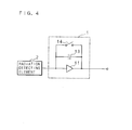
- Fig. 4 is a schematic circuit diagram of a radiation detector according to the present invention.
- the radiation detector includes a radiation detecting element 2 for detecting radiation such as X-rays.
- the radiation detecting element 2 is a semiconductor detecting element such as a SDD.
- the radiation detecting element 2 generates a charge signal in proportion to radiation energy upon entrance of radiation.
- the output terminal of the radiation detecting element 2 is connected to a preamplifier 1.
- the preamplifier 1 is an amplifier of the present invention.
- the radiation detecting element 2 outputs a charge signal, while the preamplifier 1 converts the charge signal output from the radiation detecting element 2 into a voltage signal proportionate to the energy of radiation.
- the output terminal of preamplifier 1 is connected to the output terminal of the radiation detector.
- the radiation detector is included in, for example, an X-ray detection apparatus, the output terminal of the radiation detector being connected to the signal processing unit via an amplifier in the X-ray detection apparatus.
- the voltage signal output by the radiation detector is amplified by the amplifier and processed in a signal processing unit.
- the signal processing unit counts a voltage signal for each value to obtain spectra of the detected X-rays.
- the radiation detector is included in an X-ray fluorescence spectrometer, which detects fluorescent X-rays emitted from a sample and performs an X-ray fluorescence analysis on the sample.
- the preamplifier 1 includes an amplifying circuit 11 with an input terminal thereof connected to the radiation detecting element 2. A charge signal from the radiation detecting element 2 is input to the amplifying circuit 11. The FET required for inputting signals to the amplifying circuit 11 is included in the amplifying circuit 11. Moreover, each of the feedback capacitor 13 and the reset switch 14 is connected in parallel with the amplifying circuit 11. That is, each of the capacitor 13 and switch 14 is connected between the input terminal and the output terminal of the amplifying circuit 11.
- the preamplifier 1 is configured as an integrated circuit formed as a chip.
- Fig. 5 is a schematic plan view of the preamplifier 1 formed as a chip.
- a core area 41 including the amplifying circuit 11 is provided, around which a plurality of bonding pads 43 are arranged.
- the bonding pads 43 are connected to the core area 41 and are used for supplying power, outputting a voltage signal and inputting a pulse for resetting. Any one of the bonding pads 43 is connected to the output terminal of the amplifying circuit 11 and serves as an output terminal of the preamplifier 1.
- a bonding pad 42 for input is further arranged around the core area 41.
- the boding pad 42 for input corresponds to the bonding pad in the present invention.
- the radiation detecting element 2 is connected to the bonding pad 42 through a bonding wire (not shown in Fig. 5 ).
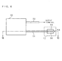
- Fig. 6 is a schematic plan view illustrating the configuration of a part of the preamplifier 1 according to Embodiment 1.
- Fig. 7 is a schematic section view along the line VII-VII in Fig. 6.
- Figs. 6 and 7 show the bonding pad 42 for input and a portion in the vicinity of the bonding pad 42.
- the preamplifier 1 has a configuration in which a circuit is integrated on a substrate 61 of Si.
- the substrate 61 and an oxide film 62 are not illustrated in Fig. 6 .
- the bonding pad 42 is formed to be connected to a bonding wire 3 connected to the radiation detecting element 2.
- Fig. 6 shows each of the components orthogonally projected to the substrate 61.
- a conductive interconnection layer 51 made of aluminum (Al) is provided below the bonding pad 42, i.e. between the bonding pad 42 and the substrate 61.
- a portion of the interconnection layer 51 located between the bonding pad 42 and the substrate 61 has a projection area orthogonal to the substrate 61 which is approximately equal to that of the bonding pad 42.
- the bonding pad 42 is substantially superposed above this portion of the interconnection layer 51 in plan view.
- the interconnection layer 51 is located below the bonding pad 42.
- An insulating oxide film 62 formed of silicon dioxide is disposed between the bonding pad 42 and the interconnection layer 51. Via holes 57 penetrating the oxide film 62 is formed between the bonding pad 42 and the interconnection layer 51, while the bonding pad 42 is connected to the interconnection layer 51 through the via holes 57.
- the interconnection layer 51 further extends in a linear form to the outside the region below the bonding pad 42.
- the extended interconnection layer 51 is connected to the gate electrode 54 formed with a poly-silicon (poly-Si) layer.
- a source electrode 55 is provided at one side of the gate electrode 54 and a drain electrode 56 is provided at the other side.
- a gate oxide film 58 is formed below the gate electrode 54, i.e. between the gate electrode 54 and the substrate 61.
- the gate oxide film 58 is in contact with the gate electrode 54 and the substrate 61.
- the gate electrode 54, source electrode 55, drain electrode 56 and gate oxide film 58 are included in a MOSFET 12 for input which is embedded in the amplifying circuit 11.
- the interconnection layer 51 is connected to the gate electrode 54 to thereby be connected to the input terminal of the amplifying circuit 11.
- the amplifying circuit 11 may be configured to include a JFET or a bipolar transistor instead of MOSFET 12.
- a conductive layer 52 formed with a conductive poly-Si layer is disposed below the interconnection layer 51, i.e. between the interconnection layer 51 and the substrate 61.
- An insulating oxide film 59 is formed between the conductive layer 52 and the substrate 61.
- a large part of the conductive layer 52 is overlapped by the bonding pad 42 in a plan view when projected orthogonally to the substrate 61. Though hidden by the bonding pad 42 in Fig. 6 , the conductive layer 52 is located below the interconnection layer 51 which is below the bonding pad 42. That is, a large part of the conductive layer 52 is arranged directly below the bonding pad 42.
- the interconnection layer 51 and the conductive layer 52 are arranged in substantially parallel with each other, while an insulating oxide film 62 is interposed between the interconnection layer 51 and the conductive layer 52. Furthermore, as indicated by the broken line in Fig. 7 , the conductive layer 52 is connected to another interconnection layer 53, which is connected to the output terminal of the amplifier 11. Except for the upper surface of the bonding pad 42, each part of the preamplifier 1 is covered with the oxide film 62. It is noted that the conductive layer 52 may be a metal interconnection layer. Furthermore, the interconnection layer 51 and the conductive layer 52 may be arranged to overlap with each other in at least a part thereof in plan view.
- the insulating oxide film 62 is interposed between the conductive interconnection layer 51 and the conductive layer 52, a capacitor, with the interconnection layer 51 and the conductive layer 52 serving as a pair of electrodes while the oxide film 62 serves as a dielectric, is formed.
- the oxide film 62 between the interconnection layer 51 and the conductive layer 52 corresponds to the insulating layer in the present invention.
- the interconnection layer 51 which is one electrode is connected to the input terminal of the amplifying circuit 11, while the conductive layer 52 which is the other electrode is connected to the output terminal of the amplifier 11 through the interconnection layer 53, which makes this capacitor be the feedback capacitor 13.
- the interconnection layer 51 connected to the bonding pad 42 serves as one electrode of the feedback capacitor 13.
- the input capacitance for the amplifying circuit 11 is reduced compared to the conventional preamplifier. It is also possible to adjust the capacitance of the feedback capacitor 13 at the time of manufacturing, by adjusting the area in which the interconnection layer 51 and conductive layer 52 overlap with each other.
- the parasitic capacitance between the interconnection layer 51 below the bonding pad 42 and, for example, the substrate 61 will be the same as that in the conventional preamplifier.
- the capacitor 13 is disposed below the bonding pad 42 with the interconnection layer 51 serving as one electrode, allowing the feedback capacitance of the capacitor 13 to be included in the parasitic capacitance between the interconnection layer 51 and, for example, the substrate 61.
- the preamplifier 1 according to the present embodiment has a reduced input capacitance for the amplifying circuit 11 by the amount of the feedback capacitance of the capacitor 13.
- the preamplifier 1 has a reduced input capacitance for the amplifying circuit 11 compared to the conventional case.
- the noise included in the signal output by the preamplifier 1 is reduced compared to the conventional case.
- the preamplifier 1 is formed at low cost while noise may sufficiently be reduced.
- the noise included in the output voltage signal is reduced compared to the conventional case, improving the energy resolution for radiation detection.
- the X-ray detection apparatus provided with the radiation detector according to the present embodiment, for example, can detect X-rays with a high resolution.
- the X-ray fluorescence spectrometer provided with the radiation detector according to the present embodiment, for example, can perform highly accurate X-ray fluorescence analysis.
- the preamplifier 1 may have a form in which only a part of the portion configuring the capacitor 13 in the interconnection layer 51 and the conductive layer 52 on the projection plane orthogonally projected to the substrate 61 is overlapped by the bonding pad 42.
- the capacitance for the capacitor 13 the capacitance for the portion overlapping the bonding pad 42 on the projection plane is included in the parasitic capacitance between the interconnection layer 51 and, for example, the substrate 61.
- the input capacitance for the amplifying circuit 11 is reduced compared to the conventional case by the amount of the capacitance for the above-described portion.
- the input capacitance for the amplifying circuit 11 is reduced compared to the conventional case also in the preamplifier 1 according to the embodiment, while the noise included in the output signal is reduced compared to the conventional case.
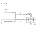
- Fig. 8 is a schematic plan view illustrating the configuration of a part of the preamplifier 1 according to Embodiment 2.
- Fig. 9 is a schematic section view along the line IX-IX in Fig. 8.
- Fig. 8 is a view formed by projecting each component orthogonally to a substrate 61, while the substrate 61 and an oxide film 62 are not shown.
- a preamplifier 1 does not include a bonding pad 42 and via holes 57.
- a part of an interconnection layer 51 forms a connection portion 511 also serving as a bonding pad.
- the connection portion 511 has an area large enough to be connected to a bonding wire 3 connected to a radiation detecting element 2.
- connection portion 511 The upper surface of the connection portion 511 is not covered with the oxide film 62, so that the connection portion 511 is connected to the bonding wire 3.
- the conductive layer 52 is interposed between the connection portion 511 of the interconnection layer 51 and the substrate 61. A large part of the conductive layer 52 overlaps the connection portion 511 in a plan view formed by orthogonal projection to the substrate 61.
- the insulating oxide film 62 is interposed between the connection portion 511 of the interconnection layer 51 and the conductive layer 52.
- the other configuration parts of the preamplifier 1 are similar to those in Embodiment 1. It is noted that the connection portion 511 and the conductive layer 52 may overlap with each other in at least a part thereof in plan view.
- a capacitor is configured with the interconnection layer 51 and the conductive layer 52 serving as a pair of electrodes and with the oxide film 62 serving as a dielectric, the capacitor corresponding to the feedback capacitor 13. Since there is no wiring for connecting the bonding pad and the capacitor 13, the parasitic capacitance generated at the conventional preamplifier due to the wiring will not be generated. Accordingly, the input capacitance for the amplifying circuit 11 is reduced compared to the case with the conventional preamplifier.
- the connection portion 511 of the interconnection layer 51 forms one electrode of the capacitor 13
- the feedback capacitance of the capacitor 13 is included in the parasitic capacitance between the interconnection layer 51 and the substrate 61.
- the preamplifier 1 Compared to the conventional preamplifier having a feedback capacitance in addition to the parasitic capacitance caused by the bonding pad, the preamplifier 1 has a reduced input capacitance for the amplifying circuit 11 by the amount of the feedback capacitance for the capacitor 13. As described above, also in the preamplifier 1 according to the present embodiment, the input capacitance for the amplifying circuit 11 is reduced compared to the conventional case, and thus the noise included in the signal output from the preamplifier 1 is also reduced compared to the conventional case.
- the radiation detector including the preamplifier 1 has an improved energy resolution for detecting radiation.
- An X-ray detection apparatus including the radiation detector can detect X-rays with high resolution.
- the preamplifier 1 may include circuit devices other than the circuit devices illustrated in Embodiments 1 and 2.
- the radiation detector of the present invention may use any other radiation detecting element which outputs charge signals in accordance with detected radiation.
Landscapes
- Engineering & Computer Science (AREA)
- Power Engineering (AREA)
- Spectroscopy & Molecular Physics (AREA)
- General Physics & Mathematics (AREA)
- High Energy & Nuclear Physics (AREA)
- Molecular Biology (AREA)
- Physics & Mathematics (AREA)
- Life Sciences & Earth Sciences (AREA)
- Health & Medical Sciences (AREA)
- Measurement Of Radiation (AREA)
- Amplifiers (AREA)
- Internal Circuitry In Semiconductor Integrated Circuit Devices (AREA)
- Light Receiving Elements (AREA)
Abstract
Description
- The present invention relates to a radiation detector, and more particularly, to an amplifier for converting a charge signal output from a radiation detecting element into a voltage signal and to a radiation detector including the amplifier.
- A radiation detector for detecting radiation such as X-rays includes a radiation detecting element like, for example, SDD (Silicon Drift Detector). The radiation detecting element outputs a charge signal in accordance with detected radiation. The charge signal is converted into a voltage signal by a preamplifier. Signal processing including spectrum generation or the like is performed based on the voltage signal.
-
Fig. 1 is a circuit diagram of a preamplifier in the conventional radiation detector. A FET (Field Effect Transistor) 72 is connected at a stage preceding an amplifyingcircuit 71. A signal from the radiation detecting element is input to the amplifyingcircuit 71 through theFET 72. Moreover, each of afeedback capacitor 73 and areset switch 74 is connected to be in parallel with the amplifyingcircuit 71 and FET 72. There are cases where the amplifyingcircuit 71 is configured with an operational amplifier and a transistor, where the amplifyingcircuit 71 is configured as an integrated circuit, and where the amplifyingcircuit 71 and FET 72 are configured as one integrated circuit. -
Fig. 2 is a schematic plan view illustrating a part of the structure of a conventional preamplifier formed as a chip.Fig. 3 is a schematic view illustrating a section of a part of the conventional preamplifier formed as a chip. A bonding pad for input is denoted by areference number 74 in the drawings. Thebonding pad 74 is connected to a bondingwire 76 further connected to a radiation detecting element. In the preamplifier, ametal wiring 75 is connected to thebonding pad 74 through an interconnection layer arranged below thebonding pad 74, while thefeedback capacitor 73 is connected to themetal wiring 75. Anelectrode 731 at the upper side of thecapacitor 73 is connected to themetal wiring 75 while anelectrode 732 at the lower side thereof is connected to an output terminal of the preamplifier. Theelectrode 731 at the upper side of thecapacitor 73 is also connected to the FET 72 through themetal wiring 75. The components in the preamplifier are formed on a silicon (Si)substrate 77 while a part excluding the upper surface of thebonding pad 74 is covered with an oxide film (not shown). Thus, the conventional preamplifier is formed as an integrated circuit. Patent Document 1 discloses an example of an integrated circuit including a bonding pad and a capacitor. - [Patent Document 1] Japanese Patent Application Laid-Open No.
2000-58765 - As shown in
Fig. 3 , the conventional preamplifier causes a parasitic capacitance between an interconnection layer below thebonding pad 74 and, for example, thesubstrate 77, and also between themetal wiring 75 and, for example, thesubstrate 77. The parasitic capacitance is also caused in each of the radiation detecting element,bonding wire 76 and FET 72. Thus, the parasitic capacitance for each of the radiation detecting element,bonding wire 76,bonding pad 74,metal wiring 75 and FET 72 as well as the feedback capacitance of thecapacitor 73 are included in the input capacitance for the amplifyingcircuit 71. As the input capacitance for the amplifying circuit becomes larger, noise included in a signal output by the preamplifier is increased. In the radiation detector including the preamplifier, the energy resolution is more deteriorated as the noise included in the signal is increased. It is thus necessary to reduce the input capacitance for the amplifying circuit to reduce the noise in order to improve the energy resolution of the radiation detector. - The present invention has been contrived in view of the above circumstances. An object of the invention is to provide an amplifier and a radiation detector with a reduced input capacitance for an amplifying circuit by making improvements in the arrangement of components in an integrated circuit.
- An amplifier according to the present invention including an amplifying circuit and a feedback capacitor connected in parallel to the amplifying circuit is characterized by including a semiconductor substrate, the amplifying circuit being configured as an integrated circuit integrated on the semiconductor substrate, and by further including: a conductive interconnection layer directly or indirectly connected to an external bonding wire; and a conductive layer arranged on a side more toward the semiconductor substrate than the interconnection layer with an insulating layer interposed between the interconnection layer and the conductive layer. The feedback capacitor is so configured that the insulating layer serves as a dielectric while the interconnection layer and the conductive layer serve as a pair of electrodes. The interconnection layer is connected to an input terminal of the amplifying circuit. The conductive layer is connected to an output terminal of the amplifying circuit.
- The amplifier according to the present invention is characterized by further including a bonding pad for connection to the external bonding wire. The interconnection layer has one part interposed between the bonding pad and the semiconductor substrate, and is connected to the bonding pad.
- The amplifier according to the present invention is characterized in that at least a part of each of the bonding pad, the interconnection layer and the conductive layer orthogonally projected to the semiconductor substrate overlap with one another.
- The amplifier according to the present invention is characterized in that the amplifying circuit includes a MOSFET connected to the input terminal.
- A radiation detector according to the present invention is characterized by comprising: a radiation detecting element for generating a charge signal at the time of detecting radiation; and an amplifier according to the present invention for receiving a charge signal generated by the radiation detecting element through a bonding wire and converting the received charge signal into a voltage signal.
- According to the present invention, in the amplifier used in the preamplifier for radiation detector, the feedback capacitor is configured with the interconnection layer connected to and located below the bonding pad for input or an interconnection layer also serving as the bonding pad and a conductive layer located below the interconnection layer with the insulating layer interposed in between. Since there is no wiring for connecting the bonding pad and the capacitor, the parasitic capacitance due to the wiring will not occur.
- According to the present invention, at least parts of the bonding pad, the interconnection layer and the conductive layer that are orthogonally projected to the substrate overlap with one another. The capacitance for the portion overlapping the bonding pad of the capacitor is included in the parasitic capacitance between the interconnection layer below the bonding pad and, for example, the substrate. The input capacitance for the amplifying circuit in the preamplifier is reduced compared the conventional case by the amount corresponding to the feedback capacitance of the capacitor included in the parasitic capacitance between the interconnection layer and, for example, the substrate.
- According to the present invention, the input capacitance for the amplifying circuit is reduced compared to the conventional case, while the noise included in the signal output from the amplifier is also reduced compared to the conventional case. In the radiation detector using the amplifier as a preamplifier, therefore, the noise included in the output voltage signal is reduced compared to the conventional case, while the energy resolution in the radiation detection is improved. The present invention can, therefore, present such beneficial effects.
-
-
Fig. 1 is a circuit diagram of a preamplifier in the conventional radiation detector; -
Fig. 2 is a schematic plan view illustrating a part of the structure of the conventional preamplifier formed as a chip; -
Fig. 3 is a schematic view illustrating a section of a part of the conventional preamplifier formed as a chip; -
Fig. 4 is a schematic circuit diagram of a radiation detector according to the present invention; -
Fig. 5 is a schematic plan view of a preamplifier 1 formed as a chip; -
Fig. 6 is a schematic plan view illustrating the configuration of a part of a preamplifier according to Embodiment 1; -
Fig. 7 is a schematic section view along the line VII-VII inFig. 6 ; -
Fig. 8 is a schematic plan view illustrating the configuration of a part of a preamplifier according to Embodiment 2; and -
Fig. 9 is a schematic section view along the line IX-IX inFig. 8 . - The present invention will now be described below in detail with reference to the drawings illustrating the embodiments thereof.
-
Fig. 4 is a schematic circuit diagram of a radiation detector according to the present invention. The radiation detector includes a radiation detecting element 2 for detecting radiation such as X-rays. The radiation detecting element 2 is a semiconductor detecting element such as a SDD. The radiation detecting element 2 generates a charge signal in proportion to radiation energy upon entrance of radiation. The output terminal of the radiation detecting element 2 is connected to a preamplifier 1. The preamplifier 1 is an amplifier of the present invention. The radiation detecting element 2 outputs a charge signal, while the preamplifier 1 converts the charge signal output from the radiation detecting element 2 into a voltage signal proportionate to the energy of radiation. The output terminal of preamplifier 1 is connected to the output terminal of the radiation detector. - The radiation detector is included in, for example, an X-ray detection apparatus, the output terminal of the radiation detector being connected to the signal processing unit via an amplifier in the X-ray detection apparatus. The voltage signal output by the radiation detector is amplified by the amplifier and processed in a signal processing unit. For example, the signal processing unit counts a voltage signal for each value to obtain spectra of the detected X-rays. In another example, the radiation detector is included in an X-ray fluorescence spectrometer, which detects fluorescent X-rays emitted from a sample and performs an X-ray fluorescence analysis on the sample.
- The preamplifier 1 includes an amplifying
circuit 11 with an input terminal thereof connected to the radiation detecting element 2. A charge signal from the radiation detecting element 2 is input to the amplifyingcircuit 11. The FET required for inputting signals to the amplifyingcircuit 11 is included in the amplifyingcircuit 11. Moreover, each of thefeedback capacitor 13 and thereset switch 14 is connected in parallel with the amplifyingcircuit 11. That is, each of thecapacitor 13 andswitch 14 is connected between the input terminal and the output terminal of the amplifyingcircuit 11. The preamplifier 1 is configured as an integrated circuit formed as a chip. -
Fig. 5 is a schematic plan view of the preamplifier 1 formed as a chip. Acore area 41 including the amplifyingcircuit 11 is provided, around which a plurality ofbonding pads 43 are arranged. Thebonding pads 43 are connected to thecore area 41 and are used for supplying power, outputting a voltage signal and inputting a pulse for resetting. Any one of thebonding pads 43 is connected to the output terminal of the amplifyingcircuit 11 and serves as an output terminal of the preamplifier 1. Abonding pad 42 for input is further arranged around thecore area 41. Theboding pad 42 for input corresponds to the bonding pad in the present invention. The radiation detecting element 2 is connected to thebonding pad 42 through a bonding wire (not shown inFig. 5 ). -
Fig. 6 is a schematic plan view illustrating the configuration of a part of the preamplifier 1 according to Embodiment 1.Fig. 7 is a schematic section view along the line VII-VII inFig. 6. Figs. 6 and7 show thebonding pad 42 for input and a portion in the vicinity of thebonding pad 42. The preamplifier 1 has a configuration in which a circuit is integrated on asubstrate 61 of Si. Thesubstrate 61 and anoxide film 62 are not illustrated inFig. 6 . Thebonding pad 42 is formed to be connected to abonding wire 3 connected to the radiation detecting element 2. Moreover,Fig. 6 shows each of the components orthogonally projected to thesubstrate 61. - A
conductive interconnection layer 51 made of aluminum (Al) is provided below thebonding pad 42, i.e. between thebonding pad 42 and thesubstrate 61. A portion of theinterconnection layer 51 located between thebonding pad 42 and thesubstrate 61 has a projection area orthogonal to thesubstrate 61 which is approximately equal to that of thebonding pad 42. Thus, thebonding pad 42 is substantially superposed above this portion of theinterconnection layer 51 in plan view. Though hidden by thebonding pad 42 inFig. 6 , theinterconnection layer 51 is located below thebonding pad 42. An insulatingoxide film 62 formed of silicon dioxide is disposed between thebonding pad 42 and theinterconnection layer 51. Viaholes 57 penetrating theoxide film 62 is formed between thebonding pad 42 and theinterconnection layer 51, while thebonding pad 42 is connected to theinterconnection layer 51 through the via holes 57. - The
interconnection layer 51 further extends in a linear form to the outside the region below thebonding pad 42. Theextended interconnection layer 51 is connected to thegate electrode 54 formed with a poly-silicon (poly-Si) layer. Asource electrode 55 is provided at one side of thegate electrode 54 and adrain electrode 56 is provided at the other side. Agate oxide film 58 is formed below thegate electrode 54, i.e. between thegate electrode 54 and thesubstrate 61. Thegate oxide film 58 is in contact with thegate electrode 54 and thesubstrate 61. Thegate electrode 54,source electrode 55,drain electrode 56 andgate oxide film 58 are included in aMOSFET 12 for input which is embedded in the amplifyingcircuit 11. In other words, theinterconnection layer 51 is connected to thegate electrode 54 to thereby be connected to the input terminal of the amplifyingcircuit 11. It is noted that the amplifyingcircuit 11 may be configured to include a JFET or a bipolar transistor instead ofMOSFET 12. - A
conductive layer 52 formed with a conductive poly-Si layer is disposed below theinterconnection layer 51, i.e. between theinterconnection layer 51 and thesubstrate 61. An insulatingoxide film 59 is formed between theconductive layer 52 and thesubstrate 61. A large part of theconductive layer 52 is overlapped by thebonding pad 42 in a plan view when projected orthogonally to thesubstrate 61. Though hidden by thebonding pad 42 inFig. 6 , theconductive layer 52 is located below theinterconnection layer 51 which is below thebonding pad 42. That is, a large part of theconductive layer 52 is arranged directly below thebonding pad 42. Moreover, theinterconnection layer 51 and theconductive layer 52 are arranged in substantially parallel with each other, while an insulatingoxide film 62 is interposed between theinterconnection layer 51 and theconductive layer 52. Furthermore, as indicated by the broken line inFig. 7 , theconductive layer 52 is connected to anotherinterconnection layer 53, which is connected to the output terminal of theamplifier 11. Except for the upper surface of thebonding pad 42, each part of the preamplifier 1 is covered with theoxide film 62. It is noted that theconductive layer 52 may be a metal interconnection layer. Furthermore, theinterconnection layer 51 and theconductive layer 52 may be arranged to overlap with each other in at least a part thereof in plan view. - Since the insulating
oxide film 62 is interposed between theconductive interconnection layer 51 and theconductive layer 52, a capacitor, with theinterconnection layer 51 and theconductive layer 52 serving as a pair of electrodes while theoxide film 62 serves as a dielectric, is formed. Theoxide film 62 between theinterconnection layer 51 and theconductive layer 52 corresponds to the insulating layer in the present invention. Theinterconnection layer 51 which is one electrode is connected to the input terminal of the amplifyingcircuit 11, while theconductive layer 52 which is the other electrode is connected to the output terminal of theamplifier 11 through theinterconnection layer 53, which makes this capacitor be thefeedback capacitor 13. - As has been described above, in the preamplifier 1, the
interconnection layer 51 connected to thebonding pad 42 serves as one electrode of thefeedback capacitor 13. Thus, there is no wiring for connecting thebonding pad 42 and thecapacitor 13, preventing the parasitic capacitance, which is generated in the conventional preamplifier due to such wiring, from being generated. Accordingly, the input capacitance for the amplifyingcircuit 11 is reduced compared to the conventional preamplifier. It is also possible to adjust the capacitance of thefeedback capacitor 13 at the time of manufacturing, by adjusting the area in which theinterconnection layer 51 andconductive layer 52 overlap with each other. - Moreover, in the present embodiment, the
bonding pad 42,interconnection layer 51 andconductive layer 52, which are projected orthogonally to thesubstrate 61, overlap with one another. It is assumed here that the area of thebonding pad 42, the area of theinterconnection layer 51 below thebonding pad 42, the thickness of theoxide film 62 between theinterconnection layer 51 and thesubstrate 61, and the permittivity of theoxide film 62 are equal to those in the conventional preamplifier. Here, the parasitic capacitance between theinterconnection layer 51 below thebonding pad 42 and, for example, thesubstrate 61 will be the same as that in the conventional preamplifier. In the preamplifier 1 according to the present embodiment, on the other hand, thecapacitor 13 is disposed below thebonding pad 42 with theinterconnection layer 51 serving as one electrode, allowing the feedback capacitance of thecapacitor 13 to be included in the parasitic capacitance between theinterconnection layer 51 and, for example, thesubstrate 61. Compared to the conventional preamplifier including a feedback capacitance in addition to the parasitic capacitance caused by the bonding pad, the preamplifier 1 according to the present embodiment has a reduced input capacitance for the amplifyingcircuit 11 by the amount of the feedback capacitance of thecapacitor 13. - As described above, the preamplifier 1 according to the present embodiment has a reduced input capacitance for the amplifying
circuit 11 compared to the conventional case. Thus, the noise included in the signal output by the preamplifier 1 is reduced compared to the conventional case. By integrating the circuit including the amplifyingcircuit 11 on thesubstrate 61, the preamplifier 1 is formed at low cost while noise may sufficiently be reduced. In the radiation detector including the preamplifier 1, the noise included in the output voltage signal is reduced compared to the conventional case, improving the energy resolution for radiation detection. Thus, the X-ray detection apparatus provided with the radiation detector according to the present embodiment, for example, can detect X-rays with a high resolution. In addition, the X-ray fluorescence spectrometer provided with the radiation detector according to the present embodiment, for example, can perform highly accurate X-ray fluorescence analysis. - Note that the preamplifier 1 may have a form in which only a part of the portion configuring the
capacitor 13 in theinterconnection layer 51 and theconductive layer 52 on the projection plane orthogonally projected to thesubstrate 61 is overlapped by thebonding pad 42. Among the capacitance for thecapacitor 13, the capacitance for the portion overlapping thebonding pad 42 on the projection plane is included in the parasitic capacitance between theinterconnection layer 51 and, for example, thesubstrate 61. Thus, the input capacitance for the amplifyingcircuit 11 is reduced compared to the conventional case by the amount of the capacitance for the above-described portion. The input capacitance for the amplifyingcircuit 11 is reduced compared to the conventional case also in the preamplifier 1 according to the embodiment, while the noise included in the output signal is reduced compared to the conventional case. -
Fig. 8 is a schematic plan view illustrating the configuration of a part of the preamplifier 1 according to Embodiment 2.Fig. 9 is a schematic section view along the line IX-IX inFig. 8. Fig. 8 is a view formed by projecting each component orthogonally to asubstrate 61, while thesubstrate 61 and anoxide film 62 are not shown. In the present embodiment, a preamplifier 1 does not include abonding pad 42 and viaholes 57. A part of aninterconnection layer 51 forms aconnection portion 511 also serving as a bonding pad. Theconnection portion 511 has an area large enough to be connected to abonding wire 3 connected to a radiation detecting element 2. The upper surface of theconnection portion 511 is not covered with theoxide film 62, so that theconnection portion 511 is connected to thebonding wire 3. Theconductive layer 52 is interposed between theconnection portion 511 of theinterconnection layer 51 and thesubstrate 61. A large part of theconductive layer 52 overlaps theconnection portion 511 in a plan view formed by orthogonal projection to thesubstrate 61. Moreover, the insulatingoxide film 62 is interposed between theconnection portion 511 of theinterconnection layer 51 and theconductive layer 52. The other configuration parts of the preamplifier 1 are similar to those in Embodiment 1. It is noted that theconnection portion 511 and theconductive layer 52 may overlap with each other in at least a part thereof in plan view. - In the present embodiment also, a capacitor is configured with the
interconnection layer 51 and theconductive layer 52 serving as a pair of electrodes and with theoxide film 62 serving as a dielectric, the capacitor corresponding to thefeedback capacitor 13. Since there is no wiring for connecting the bonding pad and thecapacitor 13, the parasitic capacitance generated at the conventional preamplifier due to the wiring will not be generated. Accordingly, the input capacitance for the amplifyingcircuit 11 is reduced compared to the case with the conventional preamplifier. In addition, as theconnection portion 511 of theinterconnection layer 51 forms one electrode of thecapacitor 13, the feedback capacitance of thecapacitor 13 is included in the parasitic capacitance between theinterconnection layer 51 and thesubstrate 61. Compared to the conventional preamplifier having a feedback capacitance in addition to the parasitic capacitance caused by the bonding pad, the preamplifier 1 has a reduced input capacitance for the amplifyingcircuit 11 by the amount of the feedback capacitance for thecapacitor 13. As described above, also in the preamplifier 1 according to the present embodiment, the input capacitance for the amplifyingcircuit 11 is reduced compared to the conventional case, and thus the noise included in the signal output from the preamplifier 1 is also reduced compared to the conventional case. The radiation detector including the preamplifier 1 has an improved energy resolution for detecting radiation. An X-ray detection apparatus including the radiation detector can detect X-rays with high resolution. - It is noted that the minimum configuration of the preamplifier 1 is described in Embodiments 1 and 2, while the preamplifier 1 may include circuit devices other than the circuit devices illustrated in Embodiments 1 and 2. Moreover, though Embodiments 1 and 2 described examples where a semiconductor detecting element is used as the radiation detecting element, the radiation detector of the present invention may use any other radiation detecting element which outputs charge signals in accordance with detected radiation.
-
- 1
- preamplifier (amplifier)
- 11
- amplifying circuit
- 12
- MOSFET
- 13
- capacitor
- 14
- switch
- 2
- radiation detecting element
- 3
- bonding wire
- 42
- bonding pad
- 51
- interconnection layer
- 52
- conductive layer
- 54
- gate electrode
- 55
- source electrode
- 56
- drain electrode
- 58
- gate oxide film
- 61
- substrate
- 62
- oxide film
Claims (5)
- An amplifier, comprising an amplifying circuit and a feedback capacitor connected in parallel to the amplifying circuit, characterized by comprising
a semiconductor substrate, wherein
the amplifying circuit is configured as an integrated circuit integrated on the semiconductor substrate,
the amplifier further comprising:a conductive interconnection layer directly or indirectly connected to an external bonding wire; anda conductive layer arranged on a side more toward the semiconductor substrate than the interconnection layer with an insulating layer interposed between the interconnection layer and the conductive layer, whereinthe feedback capacitor is so configured that the insulating layer serves as a dielectric while the interconnection layer and the conductive layer serve as a pair of electrodes,the interconnection layer is connected to an input terminal of the amplifying circuit, andthe conductive layer is connected to an output terminal of the amplifying circuit. - The amplifier according to claim 1, characterized by further comprising
a bonding pad for connection to the external bonding wire, wherein
the interconnection layer has one part interposed between the bonding pad and the semiconductor substrate, and is connected to the bonding pad. - The amplifier according to claim 2, characterized in that
at least parts of the bonding pad, the interconnection layer and the conductive layer orthogonally projected to the semiconductor substrate overlap with one another. - The amplifier according to any one of claims 1 to 3, characterized in that
the amplifying circuit includes a MOSFET connected to the input terminal. - A radiation detector, characterized by comprising:a radiation detecting element for generating a charge signal at the time of detecting radiation; andan amplifier according to any one of claims 1 to 4 for receiving a charge signal generated by the radiation detecting element through a bonding wire and converting the received charge signal into a voltage signal.
Applications Claiming Priority (2)
| Application Number | Priority Date | Filing Date | Title |
|---|---|---|---|
| JP2012172331 | 2012-08-02 | ||
| PCT/JP2013/070680 WO2014021358A1 (en) | 2012-08-02 | 2013-07-31 | Amplifier and radiation detector |
Publications (3)
| Publication Number | Publication Date |
|---|---|
| EP2882098A1 true EP2882098A1 (en) | 2015-06-10 |
| EP2882098A4 EP2882098A4 (en) | 2016-04-06 |
| EP2882098B1 EP2882098B1 (en) | 2018-12-05 |
Family
ID=50028028
Family Applications (1)
| Application Number | Title | Priority Date | Filing Date |
|---|---|---|---|
| EP13825254.9A Active EP2882098B1 (en) | 2012-08-02 | 2013-07-31 | Amplifier and radiation detector |
Country Status (4)
| Country | Link |
|---|---|
| US (2) | US9768737B2 (en) |
| EP (1) | EP2882098B1 (en) |
| JP (2) | JP6219282B2 (en) |
| WO (1) | WO2014021358A1 (en) |
Families Citing this family (6)
| Publication number | Priority date | Publication date | Assignee | Title |
|---|---|---|---|---|
| GB2491111B (en) * | 2011-05-19 | 2015-08-19 | Oxford Instr Nanotechnology Tools Ltd | Charge-sensitive amplifier |
| JP2019134293A (en) * | 2018-01-31 | 2019-08-08 | 東芝映像ソリューション株式会社 | Receiver |
| IT201800010671A1 (en) * | 2018-11-29 | 2020-05-29 | Milano Politecnico | CHARGING PRE-AMPLIFIER DEVICE AND RADIATION DETECTION DEVICE INCLUDING THE DEVICE |
| KR102180606B1 (en) * | 2018-12-05 | 2020-11-18 | 주식회사 액틴 | Apparatus for measuring radon emanation rate of construction material |
| IT201900025402A1 (en) * | 2019-12-23 | 2021-06-23 | Milano Politecnico | Radiation detection apparatus |
| EP3893391A1 (en) | 2020-04-07 | 2021-10-13 | Hitachi High-Tech Analytical Science Finland Oy | Amplifier circuit for a radiation detector |
Citations (1)
| Publication number | Priority date | Publication date | Assignee | Title |
|---|---|---|---|---|
| WO2012156748A1 (en) | 2011-05-19 | 2012-11-22 | Oxford Instruments Nanotechnology Tools Limited | Charge-sensitive amplifier |
Family Cites Families (41)
| Publication number | Priority date | Publication date | Assignee | Title |
|---|---|---|---|---|
| JPS53139959A (en) * | 1977-05-13 | 1978-12-06 | Hitachi Ltd | Amplifying circuit |
| NL8701528A (en) * | 1987-06-30 | 1989-01-16 | Philips Nv | SEMICONDUCTOR DEVICE FITTED WITH A LOAD TRANSFER. |
| GB8800949D0 (en) | 1988-01-16 | 1988-02-17 | Link Analytical Ltd | Junction field effect transistors |
| US4977367A (en) | 1988-01-28 | 1990-12-11 | Bicron Corporation | Range selector switch for ion chamber instrument |
| JPH02247593A (en) | 1989-03-20 | 1990-10-03 | Shimadzu Corp | Radiation detecting device |
| JP3008621B2 (en) | 1991-12-27 | 2000-02-14 | 株式会社島津製作所 | Radiation measurement device |
| JP3080472B2 (en) * | 1992-03-24 | 2000-08-28 | 大川 彰一 | Preamplifier for radiation detection |
| US5187380A (en) | 1992-04-09 | 1993-02-16 | General Electric Company | Low capacitance X-ray radiation detector |
| JPH06112406A (en) * | 1992-09-30 | 1994-04-22 | Toshiba Corp | Semiconductor integrated circuit |
| US5347231A (en) | 1993-02-23 | 1994-09-13 | Associated Universities, Inc. | Low noise charge sensitive preamplifier DC stabilized without a physical resistor |
| FR2714528B1 (en) * | 1993-12-27 | 1996-03-15 | Sgs Thomson Microelectronics | Integrated circuit test structure. |
| GB2298982B (en) | 1995-03-15 | 1998-11-18 | Plessey Semiconductors Ltd | Controllable filter arrangement |
| TW291595B (en) | 1995-05-30 | 1996-11-21 | At & T Corp | |
| US5602511A (en) | 1995-06-07 | 1997-02-11 | Santa Barbara Research Center | Capacitive transimpedance amplifier having dynamic compression |
| US5708392A (en) | 1996-02-16 | 1998-01-13 | Maxim Integrated Products, Inc. | Method and apparatus for providing limiting transimpedance amplification |
| JP3304801B2 (en) * | 1997-02-05 | 2002-07-22 | 日本電子株式会社 | AD conversion circuit |
| JP2900908B2 (en) | 1997-03-31 | 1999-06-02 | 日本電気株式会社 | Semiconductor device and manufacturing method thereof |
| JP3344550B2 (en) * | 1997-08-07 | 2002-11-11 | シャープ株式会社 | Light receiving amplifier |
| US6426672B1 (en) | 1997-08-28 | 2002-07-30 | General Electric Company | Means of selecting low noise performance or low power dissipation in the analog front end of a custom integrated circuit |
| JPH11122533A (en) | 1997-10-17 | 1999-04-30 | Sharp Corp | Semiconductor amplifier circuit and solid-state imaging device using the same |
| KR100294449B1 (en) | 1998-07-15 | 2001-07-12 | 윤종용 | Semiconductor integrated circuit device with capacitor formed under bonding pad |
| US6605294B2 (en) * | 1998-08-14 | 2003-08-12 | Incept Llc | Methods of using in situ hydration of hydrogel articles for sealing or augmentation of tissue or vessels |
| US6252462B1 (en) * | 1999-06-30 | 2001-06-26 | Raytheon Company | Capacitor transimpedance amplifier ( CTIA) with shared load |
| JP2002016069A (en) | 2000-06-29 | 2002-01-18 | Matsushita Electric Ind Co Ltd | Semiconductor device and method of manufacturing the same |
| US6587003B2 (en) | 2001-04-18 | 2003-07-01 | Canberra Industries. Inc. | Charge sensitive preamplifier with pulsed source reset |
| JP4501320B2 (en) | 2001-07-16 | 2010-07-14 | 株式会社デンソー | Capacitive humidity sensor |
| JP3926595B2 (en) | 2001-09-26 | 2007-06-06 | 東芝マイクロエレクトロニクス株式会社 | Semiconductor device |
| GB0201260D0 (en) | 2002-01-21 | 2002-03-06 | Europ Org For Nuclear Research | A sensing and imaging device |
| JP3998134B2 (en) * | 2002-09-13 | 2007-10-24 | シャープ株式会社 | AD converter, multi-channel AD converter, X-ray sensor module and control method thereof |
| JP2004288781A (en) | 2003-03-20 | 2004-10-14 | Matsushita Electric Ind Co Ltd | Semiconductor integrated circuit |
| JP4375077B2 (en) | 2004-03-25 | 2009-12-02 | 株式会社デンソー | Semiconductor protection device |
| JP2005327952A (en) | 2004-05-17 | 2005-11-24 | Mitsubishi Electric Corp | Power semiconductor device |
| JP4229885B2 (en) | 2004-08-18 | 2009-02-25 | 株式会社デンソー | Capacitive physical quantity detector |
| TW200732908A (en) | 2006-02-24 | 2007-09-01 | Delta Electronics Inc | Fan system and detector thereof |
| JP4844196B2 (en) * | 2006-03-30 | 2011-12-28 | 株式会社日立製作所 | Radiation detection circuit |
| JP2008028754A (en) | 2006-07-21 | 2008-02-07 | Rohm Co Ltd | Abnormality detection circuit and audio signal amplifying circuit using the same and electronic equipment |
| JP2009041942A (en) * | 2007-08-06 | 2009-02-26 | Fuji Electric Systems Co Ltd | Semiconductor radiation detector |
| JP2009111069A (en) | 2007-10-29 | 2009-05-21 | National Institute Of Information & Communication Technology | Extremely weak light detector |
| JP2012079820A (en) | 2010-09-30 | 2012-04-19 | Canon Inc | Detector and radiation detection system |
| US8817145B2 (en) * | 2012-03-30 | 2014-08-26 | BAE Systems Imaging Solutions Inc. | Hybrid CCD—CMOS camera adapted for forming images of moving scenes |
| CN104253096A (en) * | 2013-06-27 | 2014-12-31 | 鸿富锦精密工业(深圳)有限公司 | Electronic device |
-
2013
- 2013-07-31 EP EP13825254.9A patent/EP2882098B1/en active Active
- 2013-07-31 WO PCT/JP2013/070680 patent/WO2014021358A1/en not_active Ceased
- 2013-07-31 JP JP2014528184A patent/JP6219282B2/en active Active
- 2013-07-31 US US14/418,633 patent/US9768737B2/en active Active
-
2017
- 2017-09-14 US US15/704,496 patent/US10554178B2/en active Active
- 2017-09-27 JP JP2017187112A patent/JP2018014757A/en active Pending
Patent Citations (2)
| Publication number | Priority date | Publication date | Assignee | Title |
|---|---|---|---|---|
| WO2012156748A1 (en) | 2011-05-19 | 2012-11-22 | Oxford Instruments Nanotechnology Tools Limited | Charge-sensitive amplifier |
| US20150030132A1 (en) | 2011-05-19 | 2015-01-29 | Oxford Instruments Nanotechnolgy Tools Limited | Charge-sensitive amplifier |
Non-Patent Citations (1)
| Title |
|---|
| See also references of WO2014021358A1 |
Also Published As
| Publication number | Publication date |
|---|---|
| EP2882098B1 (en) | 2018-12-05 |
| JP2018014757A (en) | 2018-01-25 |
| JPWO2014021358A1 (en) | 2016-07-21 |
| EP2882098A4 (en) | 2016-04-06 |
| US9768737B2 (en) | 2017-09-19 |
| US20150214901A1 (en) | 2015-07-30 |
| JP6219282B2 (en) | 2017-10-25 |
| US10554178B2 (en) | 2020-02-04 |
| WO2014021358A1 (en) | 2014-02-06 |
| US20180006613A1 (en) | 2018-01-04 |
Similar Documents
| Publication | Publication Date | Title |
|---|---|---|
| US10554178B2 (en) | Amplifier and radiation detector | |
| US8816288B2 (en) | Radiation detector | |
| JP6393347B2 (en) | Charge detection amplifier | |
| JP2017033962A (en) | Photodetector and rider device using the same | |
| US20180076614A1 (en) | Semiconductor device and power control device | |
| JP2023036732A (en) | SILICON DRIFT RADIATION DETECTION ELEMENT, SILICON DRIFT RADIATION DETECTOR AND RADIATION DETECTION DEVICE | |
| JP2009139346A (en) | Radiation detection sensor and radiation detection sensor unit | |
| CN111373287A (en) | Radiation detector and radiation detection device | |
| US12163992B2 (en) | Charge detection sensor and potential measurement system | |
| US11604292B2 (en) | Charge preamplifier device and radiation detecting apparatus comprising the device | |
| US20190324160A1 (en) | X-ray detector and x-ray measurement device using the same | |
| US11862631B2 (en) | Radiation resistant circuit device, pressure transmission device, and nuclear power plant measurement system | |
| US10036722B2 (en) | Ion concentration measuring method and apparatus | |
| JP6143049B2 (en) | Semiconductor device | |
| JP2023173690A (en) | image sensor | |
| JP6745481B2 (en) | Infrared detector and manufacturing method thereof | |
| JP2007155561A (en) | Radiological image detection module and radiological image detection device | |
| Ratti et al. | Advantages of a vertical integration process in the design of DNW MAPS |
Legal Events
| Date | Code | Title | Description |
|---|---|---|---|
| PUAI | Public reference made under article 153(3) epc to a published international application that has entered the european phase |
Free format text: ORIGINAL CODE: 0009012 |
|
| 17P | Request for examination filed |
Effective date: 20150302 |
|
| AK | Designated contracting states |
Kind code of ref document: A1 Designated state(s): AL AT BE BG CH CY CZ DE DK EE ES FI FR GB GR HR HU IE IS IT LI LT LU LV MC MK MT NL NO PL PT RO RS SE SI SK SM TR |
|
| AX | Request for extension of the european patent |
Extension state: BA ME |
|
| DAX | Request for extension of the european patent (deleted) | ||
| RA4 | Supplementary search report drawn up and despatched (corrected) |
Effective date: 20160309 |
|
| RIC1 | Information provided on ipc code assigned before grant |
Ipc: H03F 1/26 20060101AFI20160303BHEP Ipc: G01T 1/24 20060101ALI20160303BHEP Ipc: H01L 31/09 20060101ALI20160303BHEP Ipc: G01T 1/17 20060101ALI20160303BHEP Ipc: H03F 3/70 20060101ALI20160303BHEP |
|
| STAA | Information on the status of an ep patent application or granted ep patent |
Free format text: STATUS: EXAMINATION IS IN PROGRESS |
|
| 17Q | First examination report despatched |
Effective date: 20170518 |
|
| TPAC | Observations filed by third parties |
Free format text: ORIGINAL CODE: EPIDOSNTIPA |
|
| TPAC | Observations filed by third parties |
Free format text: ORIGINAL CODE: EPIDOSNTIPA |
|
| GRAP | Despatch of communication of intention to grant a patent |
Free format text: ORIGINAL CODE: EPIDOSNIGR1 |
|
| STAA | Information on the status of an ep patent application or granted ep patent |
Free format text: STATUS: GRANT OF PATENT IS INTENDED |
|
| INTG | Intention to grant announced |
Effective date: 20180625 |
|
| GRAS | Grant fee paid |
Free format text: ORIGINAL CODE: EPIDOSNIGR3 |
|
| GRAA | (expected) grant |
Free format text: ORIGINAL CODE: 0009210 |
|
| STAA | Information on the status of an ep patent application or granted ep patent |
Free format text: STATUS: THE PATENT HAS BEEN GRANTED |
|
| AK | Designated contracting states |
Kind code of ref document: B1 Designated state(s): AL AT BE BG CH CY CZ DE DK EE ES FI FR GB GR HR HU IE IS IT LI LT LU LV MC MK MT NL NO PL PT RO RS SE SI SK SM TR |
|
| REG | Reference to a national code |
Ref country code: GB Ref legal event code: FG4D |
|
| REG | Reference to a national code |
Ref country code: CH Ref legal event code: EP |
|
| REG | Reference to a national code |
Ref country code: AT Ref legal event code: REF Ref document number: 1074331 Country of ref document: AT Kind code of ref document: T Effective date: 20181215 |
|
| REG | Reference to a national code |
Ref country code: IE Ref legal event code: FG4D |
|
| REG | Reference to a national code |
Ref country code: DE Ref legal event code: R096 Ref document number: 602013047904 Country of ref document: DE |
|
| RAP2 | Party data changed (patent owner data changed or rights of a patent transferred) |
Owner name: POLITECNICO DI MILANO Owner name: HORIBA, LTD. |
|
| REG | Reference to a national code |
Ref country code: NL Ref legal event code: MP Effective date: 20181205 |
|
| REG | Reference to a national code |
Ref country code: AT Ref legal event code: MK05 Ref document number: 1074331 Country of ref document: AT Kind code of ref document: T Effective date: 20181205 |
|
| REG | Reference to a national code |
Ref country code: LT Ref legal event code: MG4D |
|
| PG25 | Lapsed in a contracting state [announced via postgrant information from national office to epo] |
Ref country code: NO Free format text: LAPSE BECAUSE OF FAILURE TO SUBMIT A TRANSLATION OF THE DESCRIPTION OR TO PAY THE FEE WITHIN THE PRESCRIBED TIME-LIMIT Effective date: 20190305 Ref country code: LT Free format text: LAPSE BECAUSE OF FAILURE TO SUBMIT A TRANSLATION OF THE DESCRIPTION OR TO PAY THE FEE WITHIN THE PRESCRIBED TIME-LIMIT Effective date: 20181205 Ref country code: HR Free format text: LAPSE BECAUSE OF FAILURE TO SUBMIT A TRANSLATION OF THE DESCRIPTION OR TO PAY THE FEE WITHIN THE PRESCRIBED TIME-LIMIT Effective date: 20181205 Ref country code: BG Free format text: LAPSE BECAUSE OF FAILURE TO SUBMIT A TRANSLATION OF THE DESCRIPTION OR TO PAY THE FEE WITHIN THE PRESCRIBED TIME-LIMIT Effective date: 20190305 Ref country code: AT Free format text: LAPSE BECAUSE OF FAILURE TO SUBMIT A TRANSLATION OF THE DESCRIPTION OR TO PAY THE FEE WITHIN THE PRESCRIBED TIME-LIMIT Effective date: 20181205 Ref country code: ES Free format text: LAPSE BECAUSE OF FAILURE TO SUBMIT A TRANSLATION OF THE DESCRIPTION OR TO PAY THE FEE WITHIN THE PRESCRIBED TIME-LIMIT Effective date: 20181205 Ref country code: LV Free format text: LAPSE BECAUSE OF FAILURE TO SUBMIT A TRANSLATION OF THE DESCRIPTION OR TO PAY THE FEE WITHIN THE PRESCRIBED TIME-LIMIT Effective date: 20181205 Ref country code: FI Free format text: LAPSE BECAUSE OF FAILURE TO SUBMIT A TRANSLATION OF THE DESCRIPTION OR TO PAY THE FEE WITHIN THE PRESCRIBED TIME-LIMIT Effective date: 20181205 |
|
| PG25 | Lapsed in a contracting state [announced via postgrant information from national office to epo] |
Ref country code: AL Free format text: LAPSE BECAUSE OF FAILURE TO SUBMIT A TRANSLATION OF THE DESCRIPTION OR TO PAY THE FEE WITHIN THE PRESCRIBED TIME-LIMIT Effective date: 20181205 Ref country code: SE Free format text: LAPSE BECAUSE OF FAILURE TO SUBMIT A TRANSLATION OF THE DESCRIPTION OR TO PAY THE FEE WITHIN THE PRESCRIBED TIME-LIMIT Effective date: 20181205 Ref country code: RS Free format text: LAPSE BECAUSE OF FAILURE TO SUBMIT A TRANSLATION OF THE DESCRIPTION OR TO PAY THE FEE WITHIN THE PRESCRIBED TIME-LIMIT Effective date: 20181205 Ref country code: GR Free format text: LAPSE BECAUSE OF FAILURE TO SUBMIT A TRANSLATION OF THE DESCRIPTION OR TO PAY THE FEE WITHIN THE PRESCRIBED TIME-LIMIT Effective date: 20190306 |
|
| PG25 | Lapsed in a contracting state [announced via postgrant information from national office to epo] |
Ref country code: NL Free format text: LAPSE BECAUSE OF FAILURE TO SUBMIT A TRANSLATION OF THE DESCRIPTION OR TO PAY THE FEE WITHIN THE PRESCRIBED TIME-LIMIT Effective date: 20181205 |
|
| PG25 | Lapsed in a contracting state [announced via postgrant information from national office to epo] |
Ref country code: PL Free format text: LAPSE BECAUSE OF FAILURE TO SUBMIT A TRANSLATION OF THE DESCRIPTION OR TO PAY THE FEE WITHIN THE PRESCRIBED TIME-LIMIT Effective date: 20181205 Ref country code: IT Free format text: LAPSE BECAUSE OF FAILURE TO SUBMIT A TRANSLATION OF THE DESCRIPTION OR TO PAY THE FEE WITHIN THE PRESCRIBED TIME-LIMIT Effective date: 20181205 Ref country code: CZ Free format text: LAPSE BECAUSE OF FAILURE TO SUBMIT A TRANSLATION OF THE DESCRIPTION OR TO PAY THE FEE WITHIN THE PRESCRIBED TIME-LIMIT Effective date: 20181205 Ref country code: PT Free format text: LAPSE BECAUSE OF FAILURE TO SUBMIT A TRANSLATION OF THE DESCRIPTION OR TO PAY THE FEE WITHIN THE PRESCRIBED TIME-LIMIT Effective date: 20190405 |
|
| PG25 | Lapsed in a contracting state [announced via postgrant information from national office to epo] |
Ref country code: RO Free format text: LAPSE BECAUSE OF FAILURE TO SUBMIT A TRANSLATION OF THE DESCRIPTION OR TO PAY THE FEE WITHIN THE PRESCRIBED TIME-LIMIT Effective date: 20181205 Ref country code: IS Free format text: LAPSE BECAUSE OF FAILURE TO SUBMIT A TRANSLATION OF THE DESCRIPTION OR TO PAY THE FEE WITHIN THE PRESCRIBED TIME-LIMIT Effective date: 20190405 Ref country code: SM Free format text: LAPSE BECAUSE OF FAILURE TO SUBMIT A TRANSLATION OF THE DESCRIPTION OR TO PAY THE FEE WITHIN THE PRESCRIBED TIME-LIMIT Effective date: 20181205 Ref country code: EE Free format text: LAPSE BECAUSE OF FAILURE TO SUBMIT A TRANSLATION OF THE DESCRIPTION OR TO PAY THE FEE WITHIN THE PRESCRIBED TIME-LIMIT Effective date: 20181205 Ref country code: SK Free format text: LAPSE BECAUSE OF FAILURE TO SUBMIT A TRANSLATION OF THE DESCRIPTION OR TO PAY THE FEE WITHIN THE PRESCRIBED TIME-LIMIT Effective date: 20181205 |
|
| REG | Reference to a national code |
Ref country code: DE Ref legal event code: R097 Ref document number: 602013047904 Country of ref document: DE |
|
| PLBE | No opposition filed within time limit |
Free format text: ORIGINAL CODE: 0009261 |
|
| STAA | Information on the status of an ep patent application or granted ep patent |
Free format text: STATUS: NO OPPOSITION FILED WITHIN TIME LIMIT |
|
| PG25 | Lapsed in a contracting state [announced via postgrant information from national office to epo] |
Ref country code: DK Free format text: LAPSE BECAUSE OF FAILURE TO SUBMIT A TRANSLATION OF THE DESCRIPTION OR TO PAY THE FEE WITHIN THE PRESCRIBED TIME-LIMIT Effective date: 20181205 Ref country code: SI Free format text: LAPSE BECAUSE OF FAILURE TO SUBMIT A TRANSLATION OF THE DESCRIPTION OR TO PAY THE FEE WITHIN THE PRESCRIBED TIME-LIMIT Effective date: 20181205 |
|
| 26N | No opposition filed |
Effective date: 20190906 |
|
| PG25 | Lapsed in a contracting state [announced via postgrant information from national office to epo] |
Ref country code: MC Free format text: LAPSE BECAUSE OF FAILURE TO SUBMIT A TRANSLATION OF THE DESCRIPTION OR TO PAY THE FEE WITHIN THE PRESCRIBED TIME-LIMIT Effective date: 20181205 |
|
| REG | Reference to a national code |
Ref country code: CH Ref legal event code: PL |
|
| PG25 | Lapsed in a contracting state [announced via postgrant information from national office to epo] |
Ref country code: TR Free format text: LAPSE BECAUSE OF FAILURE TO SUBMIT A TRANSLATION OF THE DESCRIPTION OR TO PAY THE FEE WITHIN THE PRESCRIBED TIME-LIMIT Effective date: 20181205 |
|
| REG | Reference to a national code |
Ref country code: BE Ref legal event code: MM Effective date: 20190731 |
|
| PG25 | Lapsed in a contracting state [announced via postgrant information from national office to epo] |
Ref country code: LU Free format text: LAPSE BECAUSE OF NON-PAYMENT OF DUE FEES Effective date: 20190731 Ref country code: LI Free format text: LAPSE BECAUSE OF NON-PAYMENT OF DUE FEES Effective date: 20190731 Ref country code: CH Free format text: LAPSE BECAUSE OF NON-PAYMENT OF DUE FEES Effective date: 20190731 Ref country code: BE Free format text: LAPSE BECAUSE OF NON-PAYMENT OF DUE FEES Effective date: 20190731 |
|
| PG25 | Lapsed in a contracting state [announced via postgrant information from national office to epo] |
Ref country code: FR Free format text: LAPSE BECAUSE OF NON-PAYMENT OF DUE FEES Effective date: 20190731 |
|
| PG25 | Lapsed in a contracting state [announced via postgrant information from national office to epo] |
Ref country code: IE Free format text: LAPSE BECAUSE OF NON-PAYMENT OF DUE FEES Effective date: 20190731 |
|
| PG25 | Lapsed in a contracting state [announced via postgrant information from national office to epo] |
Ref country code: CY Free format text: LAPSE BECAUSE OF FAILURE TO SUBMIT A TRANSLATION OF THE DESCRIPTION OR TO PAY THE FEE WITHIN THE PRESCRIBED TIME-LIMIT Effective date: 20181205 |
|
| PG25 | Lapsed in a contracting state [announced via postgrant information from national office to epo] |
Ref country code: MT Free format text: LAPSE BECAUSE OF FAILURE TO SUBMIT A TRANSLATION OF THE DESCRIPTION OR TO PAY THE FEE WITHIN THE PRESCRIBED TIME-LIMIT Effective date: 20181205 Ref country code: HU Free format text: LAPSE BECAUSE OF FAILURE TO SUBMIT A TRANSLATION OF THE DESCRIPTION OR TO PAY THE FEE WITHIN THE PRESCRIBED TIME-LIMIT; INVALID AB INITIO Effective date: 20130731 |
|
| PG25 | Lapsed in a contracting state [announced via postgrant information from national office to epo] |
Ref country code: MK Free format text: LAPSE BECAUSE OF FAILURE TO SUBMIT A TRANSLATION OF THE DESCRIPTION OR TO PAY THE FEE WITHIN THE PRESCRIBED TIME-LIMIT Effective date: 20181205 |
|
| P01 | Opt-out of the competence of the unified patent court (upc) registered |
Effective date: 20230525 |
|
| PGFP | Annual fee paid to national office [announced via postgrant information from national office to epo] |
Ref country code: DE Payment date: 20250731 Year of fee payment: 13 |
|
| PGFP | Annual fee paid to national office [announced via postgrant information from national office to epo] |
Ref country code: GB Payment date: 20250722 Year of fee payment: 13 |