WO2014021358A1 - 増幅器及び放射線検出器 - Google Patents
増幅器及び放射線検出器 Download PDFInfo
- Publication number
- WO2014021358A1 WO2014021358A1 PCT/JP2013/070680 JP2013070680W WO2014021358A1 WO 2014021358 A1 WO2014021358 A1 WO 2014021358A1 JP 2013070680 W JP2013070680 W JP 2013070680W WO 2014021358 A1 WO2014021358 A1 WO 2014021358A1
- Authority
- WO
- WIPO (PCT)
- Prior art keywords
- wiring layer
- bonding pad
- amplifier
- preamplifier
- capacitor
- Prior art date
- Legal status (The legal status is an assumption and is not a legal conclusion. Google has not performed a legal analysis and makes no representation as to the accuracy of the status listed.)
- Ceased
Links
Images





Classifications
-
- H—ELECTRICITY
- H03—ELECTRONIC CIRCUITRY
- H03F—AMPLIFIERS
- H03F1/00—Details of amplifiers with only discharge tubes, only semiconductor devices or only unspecified devices as amplifying elements
- H03F1/26—Modifications of amplifiers to reduce influence of noise generated by amplifying elements
-
- G—PHYSICS
- G01—MEASURING; TESTING
- G01T—MEASUREMENT OF NUCLEAR OR X-RADIATION
- G01T1/00—Measuring X-radiation, gamma radiation, corpuscular radiation, or cosmic radiation
- G01T1/16—Measuring radiation intensity
- G01T1/17—Circuit arrangements not adapted to a particular type of detector
-
- G—PHYSICS
- G01—MEASURING; TESTING
- G01T—MEASUREMENT OF NUCLEAR OR X-RADIATION
- G01T1/00—Measuring X-radiation, gamma radiation, corpuscular radiation, or cosmic radiation
- G01T1/16—Measuring radiation intensity
- G01T1/24—Measuring radiation intensity with semiconductor detectors
-
- H—ELECTRICITY
- H03—ELECTRONIC CIRCUITRY
- H03F—AMPLIFIERS
- H03F3/00—Amplifiers with only discharge tubes or only semiconductor devices as amplifying elements
- H03F3/04—Amplifiers with only discharge tubes or only semiconductor devices as amplifying elements with semiconductor devices only
- H03F3/08—Amplifiers with only discharge tubes or only semiconductor devices as amplifying elements with semiconductor devices only controlled by light
-
- H—ELECTRICITY
- H03—ELECTRONIC CIRCUITRY
- H03F—AMPLIFIERS
- H03F3/00—Amplifiers with only discharge tubes or only semiconductor devices as amplifying elements
- H03F3/45—Differential amplifiers
- H03F3/45071—Differential amplifiers with semiconductor devices only
- H03F3/45076—Differential amplifiers with semiconductor devices only characterised by the way of implementation of the active amplifying circuit in the differential amplifier
- H03F3/45475—Differential amplifiers with semiconductor devices only characterised by the way of implementation of the active amplifying circuit in the differential amplifier using IC blocks as the active amplifying circuit
-
- H—ELECTRICITY
- H03—ELECTRONIC CIRCUITRY
- H03F—AMPLIFIERS
- H03F3/00—Amplifiers with only discharge tubes or only semiconductor devices as amplifying elements
- H03F3/70—Charge amplifiers
-
- H—ELECTRICITY
- H03—ELECTRONIC CIRCUITRY
- H03F—AMPLIFIERS
- H03F2200/00—Indexing scheme relating to amplifiers
- H03F2200/261—Amplifier which being suitable for instrumentation applications
-
- H—ELECTRICITY
- H03—ELECTRONIC CIRCUITRY
- H03F—AMPLIFIERS
- H03F2200/00—Indexing scheme relating to amplifiers
- H03F2200/372—Noise reduction and elimination in amplifier
-
- H—ELECTRICITY
- H03—ELECTRONIC CIRCUITRY
- H03F—AMPLIFIERS
- H03F2200/00—Indexing scheme relating to amplifiers
- H03F2200/411—Indexing scheme relating to amplifiers the output amplifying stage of an amplifier comprising two power stages
-
- H—ELECTRICITY
- H03—ELECTRONIC CIRCUITRY
- H03F—AMPLIFIERS
- H03F2203/00—Indexing scheme relating to amplifiers with only discharge tubes or only semiconductor devices as amplifying elements covered by H03F3/00
- H03F2203/45—Indexing scheme relating to differential amplifiers
- H03F2203/45512—Indexing scheme relating to differential amplifiers the FBC comprising one or more capacitors, not being switched capacitors, and being coupled between the LC and the IC
-
- H—ELECTRICITY
- H03—ELECTRONIC CIRCUITRY
- H03F—AMPLIFIERS
- H03F2203/00—Indexing scheme relating to amplifiers with only discharge tubes or only semiconductor devices as amplifying elements covered by H03F3/00
- H03F2203/45—Indexing scheme relating to differential amplifiers
- H03F2203/45514—Indexing scheme relating to differential amplifiers the FBC comprising one or more switched capacitors, and being coupled between the LC and the IC
-
- H—ELECTRICITY
- H03—ELECTRONIC CIRCUITRY
- H03F—AMPLIFIERS
- H03F2203/00—Indexing scheme relating to amplifiers with only discharge tubes or only semiconductor devices as amplifying elements covered by H03F3/00
- H03F2203/45—Indexing scheme relating to differential amplifiers
- H03F2203/45536—Indexing scheme relating to differential amplifiers the FBC comprising a switch and being coupled between the LC and the IC
Definitions
- the present invention relates to a radiation detector, and more particularly to an amplifier that converts a charge signal output from a radiation detection element into a voltage signal, and a radiation detector including the amplifier.
- a radiation detector that detects radiation such as X-rays includes a radiation detection element such as an SDD (Silicon Drift Detector).
- the radiation detection element outputs a charge signal corresponding to the detected radiation, the charge signal is converted into a voltage signal by a preamplifier, and signal processing such as spectrum generation is performed based on the voltage signal.
- SDD Silicon Drift Detector
- FIG. 1 is a circuit diagram of a preamplifier of a conventional radiation detector.
- An FET (Field transistor) 72 is connected to the previous stage of the amplifier circuit 71, and a signal from the radiation detection element is input to the amplifier circuit 71 via the FET 72.
- a feedback capacitor 73 and a reset switch 74 are connected in parallel to the amplifier circuit 71 and the FET 72, respectively.
- the amplifier circuit 71 is composed of an operational amplifier and a transistor
- the amplifier circuit 71 is composed of an integrated circuit
- the amplifier circuit 71 and the FET 72 are composed of one integrated circuit.
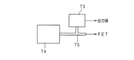
- FIG. 2 is a schematic plan view showing a part of the structure of a conventional chip preamplifier
- FIG. 3 is a schematic diagram showing a cross section of a part of the conventional chip preamplifier.
- Reference numeral 74 in the figure denotes an input bonding pad.
- a bonding wire 76 connected to the radiation detection element is connected to the bonding pad 74.
- a metal wiring 75 is connected to the bonding pad 74 via a wiring layer disposed below the bonding pad 74, and a feedback capacitor 73 is connected to the metal wiring 75.
- the upper electrode 731 of the capacitor 73 is connected to the metal wiring 75, and the lower electrode 732 is connected to the output terminal of the preamplifier.
- Patent Document 1 discloses an example of an integrated circuit including a bonding pad and a capacitor.
- the input capacitance of the amplifier circuit 71 includes the radiation detection element, the bonding wire 76, the bonding pad 74, the metal wiring 75 and the parasitic capacitance of the FET 72, and the feedback capacitance of the capacitor 73.
- the noise included in the signal output from the preamplifier increases as the input capacity of the amplifier circuit increases.
- the greater the noise contained in the signal the worse the energy resolution.
- the present invention has been made in view of such circumstances, and an object thereof is to improve an arrangement of each part in an integrated circuit, thereby reducing an input capacitance with respect to an amplifier circuit and an amplifier. It is to provide a radiation detector.
- An amplifier according to the present invention is an amplifier including an amplifier circuit and a feedback capacitor connected in parallel to the amplifier circuit.
- the amplifier includes a semiconductor substrate, and the amplifier circuit is an integrated circuit integrated on the substrate.
- the conductive wiring layer to which an external bonding wire is connected directly or indirectly, and the substrate side of the wiring layer is disposed via the insulating layer between the wiring layer and the wiring layer.
- the capacitor further includes a conductive layer, and the capacitor is configured with the insulating layer as a dielectric and the wiring layer and the conductive layer as a pair of electrodes, and the wiring layer is connected to an input end of the amplifier circuit.
- the conductive layer is connected to an output terminal of the amplifier circuit.
- the amplifier according to the present invention further includes a bonding pad for connecting the external bonding wire, and the wiring layer is partially disposed between the bonding pad and the substrate. It is characterized by being connected to.
- the amplifier according to the present invention is characterized in that at least a part of the bonding pad, the wiring layer, and the conductive layer projected perpendicularly to the substrate overlap.
- the amplifier circuit includes a MOSFET connected to the input terminal.
- the radiation detector according to the present invention includes a radiation detection element that generates a charge signal at the time of radiation detection, a charge signal generated by the radiation detection element through a bonding wire, and converts the input charge signal into a voltage signal. And an amplifier according to the invention.
- a feedback capacitor is composed of a conductive layer disposed below through an insulating layer. There is no wiring connecting the bonding pad and the capacitor, and parasitic capacitance due to this wiring does not occur.
- the bonding pad, the wiring layer, and the conductive layer projected perpendicularly to the substrate overlap.
- the capacitance of the portion overlapping the bonding pad of the capacitor is a part of the parasitic capacitance between the wiring layer below the bonding pad and, for example, the substrate.
- the amount of input capacitance to the amplifier circuit in the preamplifier is reduced as much as a part of the parasitic capacitance between the wiring layer and the substrate, for example, is used as the feedback capacitance of the capacitor.
- the input capacitance of the amplifier circuit is reduced as compared with the conventional case, and the noise included in the signal output from the amplifier is reduced as compared with the conventional case. Therefore, in a radiation detector using an amplifier as a preamplifier, the present invention has excellent effects such as a reduction in noise included in the output voltage signal compared to the conventional case and an improvement in the energy resolution of radiation detection.
- FIG. 1 is a schematic plan view of a preamplifier 1 made into a chip.
- FIG. 3 is a schematic plan view showing a partial configuration of the preamplifier according to the first embodiment.
- FIG. 7 is a schematic cross-sectional view taken along line VII-VII in FIG. 6.
- 6 is a schematic plan view showing a configuration of a part of a preamplifier according to Embodiment 2.
- FIG. 9 is a schematic cross-sectional view taken along line IX-IX in FIG. 8.
- FIG. 4 is a schematic circuit diagram of the radiation detector of the present invention.
- the radiation detector includes a radiation detection element 2 for detecting radiation such as X-rays.
- the radiation detection element 2 is a semiconductor detection element such as an SDD.
- the radiation detection element 2 generates a charge signal proportional to the energy of the radiation when the radiation is incident.
- a preamplifier 1 is connected to the output end of the radiation detection element 2.
- the preamplifier 1 is an amplifier according to the present invention.
- a charge signal is output from the radiation detection element 2, and the preamplifier 1 converts the charge signal from the radiation detection element 2 into a voltage signal proportional to the energy of the radiation.
- the output terminal of the preamplifier 1 is connected to the output terminal of the radiation detector.
- the radiation detector is provided in, for example, an X-ray detection apparatus, and the output end of the radiation detector is connected to a signal processing unit via an amplifier in the X-ray detection apparatus.
- the voltage signal output from the radiation detector is amplified by an amplifier and processed by a signal processing unit.
- the signal processing unit performs a process of counting the voltage signal of each value and acquiring the detected X-ray spectrum.
- the radiation detector is provided in a fluorescent X-ray analyzer.
- the X-ray fluorescence analyzer detects X-ray fluorescence from a sample and performs X-ray fluorescence analysis of the sample.
- the preamplifier 1 includes an amplification circuit 11, and the radiation detection element 2 is connected to the input terminal of the amplification circuit 11.
- the charge signal from the radiation detection element 2 is input to the amplifier circuit 11.
- the FET necessary for signal input to the amplifier circuit 11 is built in the amplifier circuit 11.
- Each of the feedback capacitor 13 and the reset switch 14 is connected to the amplifier circuit 11 in parallel. That is, each of the capacitor 13 and the switch 14 is connected between the input terminal and the output terminal of the amplifier circuit 11.
- the preamplifier 1 is configured as a chip integrated circuit.
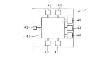
- FIG. 5 is a schematic plan view of the preamplifier 1 formed into a chip.
- a core area 41 including the amplifier circuit 11 is provided, and a plurality of bonding pads 43 are arranged around the core area 41.
- the plurality of bonding pads 43 are connected to the core area 41 and are used to supply power, output voltage signals, and input reset pulses. Any one of the plurality of bonding pads 43 is connected to the output terminal of the amplifier circuit 11 and serves as the output terminal of the preamplifier 1.
- An input bonding pad 42 is further disposed around the core area 41.
- the bonding pad 42 for input corresponds to the bonding pad in the present invention.
- the radiation detection element 2 is connected to the bonding pad 42 via a bonding wire (not shown in FIG. 5).
- FIG. 6 is a schematic plan view showing a partial configuration of the preamplifier 1 according to the first embodiment
- FIG. 7 is a schematic cross-sectional view taken along the line VII-VII in FIG. 6 and 7 show an input bonding pad 42 and a portion in the vicinity of the bonding pad 42.
- the preamplifier 1 has a configuration in which circuits are integrated on a Si substrate 61, and the substrate 61 and the oxide film 62 are omitted in FIG.
- a bonding wire 3 connected to the radiation detection element 2 is connected to the bonding pad 42.
- FIG. 6 is a diagram in which each part is projected perpendicularly to the substrate 61.
- a conductive wiring layer 51 made of Al (aluminum) is provided below the bonding pad 42, that is, between the bonding pad 42 and the substrate 61.
- a portion of the wiring layer 51 between the bonding pad 42 and the substrate 61 has a projected area perpendicular to the substrate 61 substantially equal to that of the bonding pad 42. For this reason, this portion of the wiring layer 51 substantially overlaps under the bonding pad 42 in plan view.
- An insulating oxide film 62 made of silicon dioxide exists between the bonding pad 42 and the wiring layer 51.
- a via 57 penetrating the oxide film 62 between the bonding pad 42 and the wiring layer 51 is provided, and the bonding pad 42 is connected to the wiring layer 51 through the via 57.
- the wiring layer 51 is further linearly extended outside the area below the bonding pad 42.
- the extended wiring layer 51 is connected to a gate electrode 54 formed of a poly Si (polysilicon) layer.
- a source electrode 55 and a drain electrode 56 are provided on both sides of the gate electrode 54.
- a gate oxide film 58 is provided below the gate electrode 54, that is, between the gate electrode 54 and the substrate 61.
- the gate oxide film 58 is in contact with the gate electrode 54 and the substrate 61.
- the gate electrode 54, the source electrode 55, the drain electrode 56, and the gate oxide film 58 are included in the input MOSFET 12 built in the amplifier circuit 11. That is, the wiring layer 51 is connected to the input terminal of the amplifier circuit 11 by being connected to the gate electrode 54.
- the amplifier circuit 11 may include a JFET or a bipolar transistor instead of the MOSFET 12.
- a conductive layer 52 formed of a conductive poly-Si layer is disposed below the wiring layer 51, that is, between the wiring layer 51 and the substrate 61.
- An insulating oxide film 59 is provided between the conductive layer 52 and the substrate 61.
- the conductive layer 52 substantially overlaps the bonding pad 42 in a plan view projected perpendicularly to the substrate 61. In FIG. 6, although hidden behind the bonding pad 42 and invisible, the conductive layer 52 overlaps the wiring layer 51 below the bonding pad 42. That is, the conductive layer 52 is disposed almost directly below the bonding pad 42.
- the wiring layer 51 and the conductive layer 52 are substantially parallel, and an insulating oxide film 62 exists between the wiring layer 51 and the conductive layer 52.
- another wiring layer 53 is connected to the conductive layer 52, and the wiring layer 53 is connected to the output terminal of the amplifier 11. Except for the upper surface of the bonding pad 42, each part of the preamplifier 1 is covered with an oxide film 62.
- the conductive layer 52 may be a metal wiring layer.
- the wiring layer 51 and the conductive layer 52 only have to overlap at least partially in plan view.
- a capacitor is formed using the oxide film 62 as a dielectric and the wiring layer 51 and the conductive layer 52 as a pair of electrodes.
- the oxide film 62 between the wiring layer 51 and the conductive layer 52 corresponds to the insulating layer in the present invention. Since the wiring layer 51 as one electrode is connected to the input terminal of the amplifier circuit 11 and the conductive layer 52 as the other electrode is connected to the output terminal of the amplifier 11 through the wiring layer 53, this capacitor is used for feedback. This is a capacitor 13.
- the wiring layer 51 connected to the bonding pad 42 is one electrode of the feedback capacitor 13. For this reason, there is no wiring for connecting the bonding pad 42 and the capacitor 13, and this wiring does not generate a parasitic capacitance generated in the conventional preamplifier. Therefore, the input capacitance of the amplifier circuit 11 is reduced as compared with the conventional preamplifier. It is also possible to adjust the capacitance of the feedback capacitor 13 by adjusting the area where the wiring layer 51 and the conductive layer 52 overlap during manufacturing.
- the bonding pad 42, the wiring layer 51, and the conductive layer 52 projected perpendicularly to the substrate 61 are overlapped.
- the area of the bonding pad 42, the area of the wiring layer 51 below the bonding pad 42, the thickness of the oxide film 62 between the wiring layer 51 and the substrate 61, and the oxide film 62. are assumed to have the same dielectric constant.
- the parasitic capacitance between the wiring layer 51 below the bonding pad 42 and, for example, the substrate 61 becomes an equivalent value.
- the capacitor 13 is arranged below the bonding pad 42 with the wiring layer 51 as one electrode, the parasitic capacitance between the wiring layer 51 and, for example, the substrate 61 is reduced. A part is used as the feedback capacitance of the capacitor 13.
- the input capacitance of the amplifier circuit 11 is reduced by the feedback capacitance of the capacitor 13 as compared with the conventional preamplifier 1 in which the feedback capacitance exists in addition to the parasitic capacitance caused by the bonding pad.
- the input capacitance of the amplifier circuit 11 is reduced as compared with the prior art. For this reason, the noise contained in the signal which the preamplifier 1 outputs is reduced compared with the past.
- the noise included in the output voltage signal is reduced as compared with the conventional case, and the energy resolution of radiation detection is improved. Therefore, for example, the X-ray detection apparatus including the radiation detector according to the present embodiment can detect X-rays with high resolution.
- a fluorescent X-ray analysis apparatus provided with the radiation detector according to the present embodiment enables high-precision fluorescent X-ray analysis.
- the preamplifier 1 may have a configuration in which only a part of the portion constituting the capacitor 13 of the wiring layer 51 and the conductive layer 52 overlaps the bonding pad 42 on the projection plane projected perpendicularly to the substrate 61. Good. Of the capacitance of the capacitor 13, the capacitance of the portion overlapping the bonding pad 42 on the projection plane is a part of the parasitic capacitance between the wiring layer 51 and the substrate 61, for example. For this reason, the input capacity of the amplifier circuit 11 is reduced by this capacity compared to the prior art. Therefore, also in the preamplifier 1 according to this embodiment, the input capacitance of the amplifier circuit 11 is reduced as compared with the conventional case, and the noise included in the output signal is reduced as compared with the conventional case.
- FIG. 8 is a schematic plan view showing a partial configuration of the preamplifier 1 according to the second embodiment
- FIG. 9 is a schematic cross-sectional view taken along line IX-IX in FIG.
- FIG. 8 is a diagram in which each part is projected perpendicularly to the substrate 61, and the substrate 61 and the oxide film 62 are omitted.
- the preamplifier 1 does not include the bonding pad 42 and the via 57.
- a part of the wiring layer 51 is a connection portion 511 that also serves as a bonding pad.
- the connection portion 511 has a sufficient area for connecting the bonding wire 3 connected to the radiation detection element 2. is doing.
- connection portion 511 The upper surface of the connection portion 511 is not covered with the oxide film 62, and the bonding wire 3 is connected to the connection portion 511.
- a conductive layer 52 is disposed between the connection portion 511 of the wiring layer 51 and the substrate 61.
- the conductive layer 52 substantially overlaps the connection portion 511 in a plan view projected perpendicularly to the substrate 61.
- an insulating oxide film 62 exists between the connection portion 511 of the wiring layer 51 and the conductive layer 52.
- Other configurations of the preamplifier 1 are the same as those in the first embodiment. Note that the connection portion 511 and the conductive layer 52 may overlap at least partially in plan view.
- a capacitor is formed using the oxide film 62 as a dielectric and the wiring layer 51 and the conductive layer 52 as a pair of electrodes, and this capacitor is the feedback capacitor 13.
- this capacitor is the feedback capacitor 13.
- the capacitor 13 has the connection portion 511 of the wiring layer 51 as one electrode, the feedback capacitance of the capacitor 13 is a part of the parasitic capacitance between the wiring layer 51 and, for example, the substrate 61. This is used as the feedback capacitance of the capacitor 13.
- the input capacitance of the amplifier circuit 11 is reduced by the feedback capacitance of the capacitor 13 as compared with the conventional preamplifier in which the feedback capacitance exists separately from the parasitic capacitance caused by the bonding pad.
- the input capacitance of the amplifier circuit 11 is reduced as compared with the conventional case, and the noise included in the signal output from the preamplifier 1 is reduced as compared with the conventional case.
- the radiation detector including the preamplifier 1 improves the energy resolution of radiation detection, and the X-ray detection apparatus including the radiation detector can detect X-rays with high resolution.
- the minimum configuration of the preamplifier 1 is shown.
- the preamplifier 1 may include a circuit element other than the circuit elements shown in the first and second embodiments. Good.
- Embodiments 1 and 2 an example in which a semiconductor detection element is used as a radiation detection element has been described.
- the radiation detector of the present invention is an element that outputs a charge signal corresponding to detected radiation. The form using another radiation detection element may be sufficient.
Landscapes
- Engineering & Computer Science (AREA)
- Power Engineering (AREA)
- Spectroscopy & Molecular Physics (AREA)
- General Physics & Mathematics (AREA)
- High Energy & Nuclear Physics (AREA)
- Molecular Biology (AREA)
- Physics & Mathematics (AREA)
- Life Sciences & Earth Sciences (AREA)
- Health & Medical Sciences (AREA)
- Measurement Of Radiation (AREA)
- Amplifiers (AREA)
- Internal Circuitry In Semiconductor Integrated Circuit Devices (AREA)
- Light Receiving Elements (AREA)
Abstract
Description
本発明に係る増幅器は、前記増幅回路は、前記入力端に接続されたMOSFETを内蔵していることを特徴とする。
(実施の形態1)
図4は、本発明の放射線検出器の模式的回路図である。放射線検出器は、X線等の放射線を検出するための放射線検出素子2を備えている。放射線検出素子2は、SDD等の半導体検出素子である。放射線検出素子2は、放射線が入射した場合に、放射線のエネルギーに比例した電荷信号を発生する。放射線検出素子2の出力端には、プリアンプ1が接続されている。プリアンプ1は本発明の増幅器である。放射線検出素子2からは電荷信号が出力され、プリアンプ1は、放射線検出素子2からの電荷信号を、放射線のエネルギーに比例した電圧信号に変換する。プリアンプ1の出力端には、放射線検出器の出力端子が接続されている。
図8は、実施の形態2に係るプリアンプ1の一部の構成を示す模式的平面図であり、図9は、図8のIX-IX線の模式的断面図である。図8は、基板61に垂直に各部分を投影した図になっており、基板61及び酸化膜62を省略している。本実施の形態においては、プリアンプ1は、ボンディングパッド42及びビア57を備えていない。配線層51の一部は、ボンディングパッドの役割を兼ねた接続部分511になっており、接続部分511は、放射線検出素子2に接続されたボンディングワイヤ3が接続されるために十分な面積を有している。接続部分511の上面は酸化膜62に覆われておらず、接続部分511にボンディングワイヤ3が接続されるようになっている。配線層51の接続部分511と基板61との間には、導電層52が配置されている。導電層52は、基板61に垂直に投影した平面視で接続部分511とほぼ重なっている。また、配線層51の接続部分511と導電層52との間には、絶縁性の酸化膜62が存在している。プリアンプ1のその他の構成は、実施の形態1と同様である。なお、接続部分511と導電層52とは平面視で少なくとも一部が重なっていればよい。
11 増幅回路
12 MOSFET
13 キャパシタ
14 スイッチ
2 放射線検出素子
3 ボンディングワイヤ
42 ボンディングパッド
51 配線層
52 導電層
54 ゲート電極
55 ソース電極
56 ドレイン電極
58 ゲート酸化膜
61 基板
62 酸化膜
Claims (5)
- 増幅回路と、該増幅回路に並列に接続された帰還用のキャパシタとを含む増幅器において、
半導体の基板を備え、
前記増幅回路は、前記基板上に集積された集積回路として構成されており、
外部のボンディングワイヤが直接又は間接に接続される導電性の配線層と、
該配線層よりも前記基板側に、前記配線層との間に絶縁層を介して配置された導電層とを更に備え、
前記キャパシタは、前記絶縁層を誘電体とし前記配線層及び前記導電層を一対の電極として構成されており、
前記配線層は前記増幅回路の入力端に接続されており、
前記導電層は前記増幅回路の出力端に接続されていること
を特徴とする増幅器。 - 前記外部のボンディングワイヤが接続されるためのボンディングパッドを更に備え、
前記配線層は、
前記ボンディングパッドと前記基板との間に一部が配置されており、前記ボンディングパッドに接続されていること
を特徴とする請求項1に記載の増幅器。 - 前記基板に垂直に投影した前記ボンディングパッド、前記配線層及び前記導電層の少なくとも一部が重なっていること
を特徴とする請求項2に記載の増幅器。 - 前記増幅回路は、前記入力端に接続されたMOSFETを内蔵していること
を特徴とする請求項1乃至3の何れか一つに記載の増幅器。 - 放射線検出時に電荷信号を発生する放射線検出素子と、
該放射線検出素子が発生した電荷信号をボンディングワイヤを通じて入力され、入力された電荷信号を電圧信号に変換する請求項1乃至4の何れか一つに記載の増幅器と
を備えることを特徴とする放射線検出器。
Priority Applications (4)
| Application Number | Priority Date | Filing Date | Title |
|---|---|---|---|
| JP2014528184A JP6219282B2 (ja) | 2012-08-02 | 2013-07-31 | 増幅器及び放射線検出器 |
| US14/418,633 US9768737B2 (en) | 2012-08-02 | 2013-07-31 | Amplifier and radiation detector |
| EP13825254.9A EP2882098B1 (en) | 2012-08-02 | 2013-07-31 | Amplifier and radiation detector |
| US15/704,496 US10554178B2 (en) | 2012-08-02 | 2017-09-14 | Amplifier and radiation detector |
Applications Claiming Priority (2)
| Application Number | Priority Date | Filing Date | Title |
|---|---|---|---|
| JP2012-172331 | 2012-08-02 | ||
| JP2012172331 | 2012-08-02 |
Related Child Applications (2)
| Application Number | Title | Priority Date | Filing Date |
|---|---|---|---|
| US14/418,633 A-371-Of-International US9768737B2 (en) | 2012-08-02 | 2013-07-31 | Amplifier and radiation detector |
| US15/704,496 Division US10554178B2 (en) | 2012-08-02 | 2017-09-14 | Amplifier and radiation detector |
Publications (1)
| Publication Number | Publication Date |
|---|---|
| WO2014021358A1 true WO2014021358A1 (ja) | 2014-02-06 |
Family
ID=50028028
Family Applications (1)
| Application Number | Title | Priority Date | Filing Date |
|---|---|---|---|
| PCT/JP2013/070680 Ceased WO2014021358A1 (ja) | 2012-08-02 | 2013-07-31 | 増幅器及び放射線検出器 |
Country Status (4)
| Country | Link |
|---|---|
| US (2) | US9768737B2 (ja) |
| EP (1) | EP2882098B1 (ja) |
| JP (2) | JP6219282B2 (ja) |
| WO (1) | WO2014021358A1 (ja) |
Cited By (2)
| Publication number | Priority date | Publication date | Assignee | Title |
|---|---|---|---|---|
| JP2018137828A (ja) * | 2011-05-19 | 2018-08-30 | オックスフォード インストルメンツ ナノテクノロジー ツールス リミテッド | 電荷検出増幅器 |
| JP2022509203A (ja) * | 2018-11-29 | 2022-01-20 | ポリテクニコ ディ ミラノ | 電荷前置増幅器デバイス、及び該デバイスを備える放射検出装置 |
Families Citing this family (4)
| Publication number | Priority date | Publication date | Assignee | Title |
|---|---|---|---|---|
| JP2019134293A (ja) * | 2018-01-31 | 2019-08-08 | 東芝映像ソリューション株式会社 | 受信機 |
| KR102180606B1 (ko) * | 2018-12-05 | 2020-11-18 | 주식회사 액틴 | 건축자재의 라돈방출율 측정장치 |
| IT201900025402A1 (it) * | 2019-12-23 | 2021-06-23 | Milano Politecnico | Apparato di rivelazione di radiazioni |
| EP3893391A1 (en) | 2020-04-07 | 2021-10-13 | Hitachi High-Tech Analytical Science Finland Oy | Amplifier circuit for a radiation detector |
Citations (6)
| Publication number | Priority date | Publication date | Assignee | Title |
|---|---|---|---|---|
| JPH10275824A (ja) * | 1997-03-31 | 1998-10-13 | Nec Corp | 半導体装置およびその製造方法 |
| JPH11122533A (ja) * | 1997-10-17 | 1999-04-30 | Sharp Corp | 半導体増幅回路及びそれを用いた固体撮像素子 |
| JP2000058765A (ja) | 1998-07-15 | 2000-02-25 | Samsung Electronics Co Ltd | 半導体集積回路装置 |
| JP2003100884A (ja) * | 2001-09-26 | 2003-04-04 | Toshiba Microelectronics Corp | 半導体装置 |
| JP2009111069A (ja) * | 2007-10-29 | 2009-05-21 | National Institute Of Information & Communication Technology | 極微弱光検出器 |
| JP2012079820A (ja) * | 2010-09-30 | 2012-04-19 | Canon Inc | 検出装置及び放射線検出システム |
Family Cites Families (36)
| Publication number | Priority date | Publication date | Assignee | Title |
|---|---|---|---|---|
| JPS53139959A (en) * | 1977-05-13 | 1978-12-06 | Hitachi Ltd | Amplifying circuit |
| NL8701528A (nl) * | 1987-06-30 | 1989-01-16 | Philips Nv | Halfgeleiderinrichting voozien van een ladingsoverdrachtinrichting. |
| GB8800949D0 (en) | 1988-01-16 | 1988-02-17 | Link Analytical Ltd | Junction field effect transistors |
| US4977367A (en) | 1988-01-28 | 1990-12-11 | Bicron Corporation | Range selector switch for ion chamber instrument |
| JPH02247593A (ja) | 1989-03-20 | 1990-10-03 | Shimadzu Corp | 放射線検出装置 |
| JP3008621B2 (ja) | 1991-12-27 | 2000-02-14 | 株式会社島津製作所 | 放射線測定装置 |
| JP3080472B2 (ja) * | 1992-03-24 | 2000-08-28 | 大川 彰一 | 放射線検出用前置増幅器 |
| US5187380A (en) | 1992-04-09 | 1993-02-16 | General Electric Company | Low capacitance X-ray radiation detector |
| JPH06112406A (ja) * | 1992-09-30 | 1994-04-22 | Toshiba Corp | 半導体集積回路 |
| US5347231A (en) | 1993-02-23 | 1994-09-13 | Associated Universities, Inc. | Low noise charge sensitive preamplifier DC stabilized without a physical resistor |
| FR2714528B1 (fr) * | 1993-12-27 | 1996-03-15 | Sgs Thomson Microelectronics | Structure de test de circuit intégré. |
| GB2298982B (en) | 1995-03-15 | 1998-11-18 | Plessey Semiconductors Ltd | Controllable filter arrangement |
| TW291595B (ja) | 1995-05-30 | 1996-11-21 | At & T Corp | |
| US5602511A (en) | 1995-06-07 | 1997-02-11 | Santa Barbara Research Center | Capacitive transimpedance amplifier having dynamic compression |
| US5708392A (en) | 1996-02-16 | 1998-01-13 | Maxim Integrated Products, Inc. | Method and apparatus for providing limiting transimpedance amplification |
| JP3304801B2 (ja) * | 1997-02-05 | 2002-07-22 | 日本電子株式会社 | Ad変換回路 |
| JP3344550B2 (ja) * | 1997-08-07 | 2002-11-11 | シャープ株式会社 | 受光増幅装置 |
| US6426672B1 (en) | 1997-08-28 | 2002-07-30 | General Electric Company | Means of selecting low noise performance or low power dissipation in the analog front end of a custom integrated circuit |
| US6605294B2 (en) * | 1998-08-14 | 2003-08-12 | Incept Llc | Methods of using in situ hydration of hydrogel articles for sealing or augmentation of tissue or vessels |
| US6252462B1 (en) * | 1999-06-30 | 2001-06-26 | Raytheon Company | Capacitor transimpedance amplifier ( CTIA) with shared load |
| JP2002016069A (ja) | 2000-06-29 | 2002-01-18 | Matsushita Electric Ind Co Ltd | 半導体装置およびその製造方法 |
| US6587003B2 (en) | 2001-04-18 | 2003-07-01 | Canberra Industries. Inc. | Charge sensitive preamplifier with pulsed source reset |
| JP4501320B2 (ja) | 2001-07-16 | 2010-07-14 | 株式会社デンソー | 容量式湿度センサ |
| GB0201260D0 (en) | 2002-01-21 | 2002-03-06 | Europ Org For Nuclear Research | A sensing and imaging device |
| JP3998134B2 (ja) * | 2002-09-13 | 2007-10-24 | シャープ株式会社 | Ad変換装置、多チャンネルad変換装置、x線センサーモジュールおよびそれらの制御方法 |
| JP2004288781A (ja) | 2003-03-20 | 2004-10-14 | Matsushita Electric Ind Co Ltd | 半導体集積回路 |
| JP4375077B2 (ja) | 2004-03-25 | 2009-12-02 | 株式会社デンソー | 半導体保護装置 |
| JP2005327952A (ja) | 2004-05-17 | 2005-11-24 | Mitsubishi Electric Corp | 電力用半導体装置 |
| JP4229885B2 (ja) | 2004-08-18 | 2009-02-25 | 株式会社デンソー | 容量式物理量検出装置 |
| TW200732908A (en) | 2006-02-24 | 2007-09-01 | Delta Electronics Inc | Fan system and detector thereof |
| JP4844196B2 (ja) * | 2006-03-30 | 2011-12-28 | 株式会社日立製作所 | 放射線検出回路 |
| JP2008028754A (ja) | 2006-07-21 | 2008-02-07 | Rohm Co Ltd | 異常検出回路ならびにそれを用いたオーディオ信号増幅回路および電子機器 |
| JP2009041942A (ja) * | 2007-08-06 | 2009-02-26 | Fuji Electric Systems Co Ltd | 半導体放射線検出器 |
| GB2491111B (en) * | 2011-05-19 | 2015-08-19 | Oxford Instr Nanotechnology Tools Ltd | Charge-sensitive amplifier |
| US8817145B2 (en) * | 2012-03-30 | 2014-08-26 | BAE Systems Imaging Solutions Inc. | Hybrid CCD—CMOS camera adapted for forming images of moving scenes |
| CN104253096A (zh) * | 2013-06-27 | 2014-12-31 | 鸿富锦精密工业(深圳)有限公司 | 电子设备 |
-
2013
- 2013-07-31 EP EP13825254.9A patent/EP2882098B1/en active Active
- 2013-07-31 WO PCT/JP2013/070680 patent/WO2014021358A1/ja not_active Ceased
- 2013-07-31 JP JP2014528184A patent/JP6219282B2/ja active Active
- 2013-07-31 US US14/418,633 patent/US9768737B2/en active Active
-
2017
- 2017-09-14 US US15/704,496 patent/US10554178B2/en active Active
- 2017-09-27 JP JP2017187112A patent/JP2018014757A/ja active Pending
Patent Citations (6)
| Publication number | Priority date | Publication date | Assignee | Title |
|---|---|---|---|---|
| JPH10275824A (ja) * | 1997-03-31 | 1998-10-13 | Nec Corp | 半導体装置およびその製造方法 |
| JPH11122533A (ja) * | 1997-10-17 | 1999-04-30 | Sharp Corp | 半導体増幅回路及びそれを用いた固体撮像素子 |
| JP2000058765A (ja) | 1998-07-15 | 2000-02-25 | Samsung Electronics Co Ltd | 半導体集積回路装置 |
| JP2003100884A (ja) * | 2001-09-26 | 2003-04-04 | Toshiba Microelectronics Corp | 半導体装置 |
| JP2009111069A (ja) * | 2007-10-29 | 2009-05-21 | National Institute Of Information & Communication Technology | 極微弱光検出器 |
| JP2012079820A (ja) * | 2010-09-30 | 2012-04-19 | Canon Inc | 検出装置及び放射線検出システム |
Non-Patent Citations (1)
| Title |
|---|
| See also references of EP2882098A1 |
Cited By (2)
| Publication number | Priority date | Publication date | Assignee | Title |
|---|---|---|---|---|
| JP2018137828A (ja) * | 2011-05-19 | 2018-08-30 | オックスフォード インストルメンツ ナノテクノロジー ツールス リミテッド | 電荷検出増幅器 |
| JP2022509203A (ja) * | 2018-11-29 | 2022-01-20 | ポリテクニコ ディ ミラノ | 電荷前置増幅器デバイス、及び該デバイスを備える放射検出装置 |
Also Published As
| Publication number | Publication date |
|---|---|
| EP2882098B1 (en) | 2018-12-05 |
| JP2018014757A (ja) | 2018-01-25 |
| JPWO2014021358A1 (ja) | 2016-07-21 |
| EP2882098A4 (en) | 2016-04-06 |
| US9768737B2 (en) | 2017-09-19 |
| US20150214901A1 (en) | 2015-07-30 |
| EP2882098A1 (en) | 2015-06-10 |
| JP6219282B2 (ja) | 2017-10-25 |
| US10554178B2 (en) | 2020-02-04 |
| US20180006613A1 (en) | 2018-01-04 |
Similar Documents
| Publication | Publication Date | Title |
|---|---|---|
| JP2018014757A (ja) | 増幅器及び放射線検出器 | |
| JP6393347B2 (ja) | 電荷検出増幅器 | |
| US8816288B2 (en) | Radiation detector | |
| JP7197506B2 (ja) | シリコンドリフト型放射線検出素子、シリコンドリフト型放射線検出器及び放射線検出装置 | |
| JP7132946B2 (ja) | 放射線検出器及び放射線検出装置 | |
| JP2014519261A5 (ja) | ||
| JP7441033B2 (ja) | 放射線撮像装置および放射線撮像システム | |
| US11604292B2 (en) | Charge preamplifier device and radiation detecting apparatus comprising the device | |
| US20190324160A1 (en) | X-ray detector and x-ray measurement device using the same | |
| Perić et al. | Hybrid pixel detector based on capacitive chip to chip signal-transmission | |
| JP2023173690A (ja) | イメージセンサ | |
| JP2019056581A (ja) | 電荷検出センサおよび電位計測システム | |
| JP2014165777A (ja) | X線画像検出装置およびその欠陥画素判定方法 | |
| JP2015021843A (ja) | 放射線検出器、放射線検出装置及び放射線分析装置 | |
| JP2013201309A (ja) | 半導体光センサ装置 | |
| CN118228675A (zh) | 放大器版图结构及辐射探测装置 | |
| US20130062721A1 (en) | Semiconductor strip detector | |
| Sabbah | A Solid-State Ion Detector for Use in Portable Mass Spectrometry | |
| JPH04157394A (ja) | 半導体放射線検出装置 |
Legal Events
| Date | Code | Title | Description |
|---|---|---|---|
| 121 | Ep: the epo has been informed by wipo that ep was designated in this application |
Ref document number: 13825254 Country of ref document: EP Kind code of ref document: A1 |
|
| ENP | Entry into the national phase |
Ref document number: 2014528184 Country of ref document: JP Kind code of ref document: A |
|
| WWE | Wipo information: entry into national phase |
Ref document number: 14418633 Country of ref document: US |
|
| NENP | Non-entry into the national phase |
Ref country code: DE |
|
| WWE | Wipo information: entry into national phase |
Ref document number: 2013825254 Country of ref document: EP |