EP2883207B1 - Identification automatique de matériaux à couche mince en quelques couches et/ou mono-couche - Google Patents
Identification automatique de matériaux à couche mince en quelques couches et/ou mono-couche Download PDFInfo
- Publication number
- EP2883207B1 EP2883207B1 EP13755943.1A EP13755943A EP2883207B1 EP 2883207 B1 EP2883207 B1 EP 2883207B1 EP 13755943 A EP13755943 A EP 13755943A EP 2883207 B1 EP2883207 B1 EP 2883207B1
- Authority
- EP
- European Patent Office
- Prior art keywords
- colour component
- colour
- thin
- digital image
- film material
- Prior art date
- Legal status (The legal status is an assumption and is not a legal conclusion. Google has not performed a legal analysis and makes no representation as to the accuracy of the status listed.)
- Not-in-force
Links
Images




Classifications
-
- G—PHYSICS
- G06—COMPUTING OR CALCULATING; COUNTING
- G06T—IMAGE DATA PROCESSING OR GENERATION, IN GENERAL
- G06T7/00—Image analysis
- G06T7/90—Determination of colour characteristics
-
- G—PHYSICS
- G06—COMPUTING OR CALCULATING; COUNTING
- G06T—IMAGE DATA PROCESSING OR GENERATION, IN GENERAL
- G06T7/00—Image analysis
- G06T7/10—Segmentation; Edge detection
- G06T7/12—Edge-based segmentation
-
- G—PHYSICS
- G06—COMPUTING OR CALCULATING; COUNTING
- G06T—IMAGE DATA PROCESSING OR GENERATION, IN GENERAL
- G06T2207/00—Indexing scheme for image analysis or image enhancement
- G06T2207/10—Image acquisition modality
- G06T2207/10016—Video; Image sequence
-
- G—PHYSICS
- G06—COMPUTING OR CALCULATING; COUNTING
- G06T—IMAGE DATA PROCESSING OR GENERATION, IN GENERAL
- G06T2207/00—Indexing scheme for image analysis or image enhancement
- G06T2207/10—Image acquisition modality
- G06T2207/10024—Color image
-
- G—PHYSICS
- G06—COMPUTING OR CALCULATING; COUNTING
- G06T—IMAGE DATA PROCESSING OR GENERATION, IN GENERAL
- G06T2207/00—Indexing scheme for image analysis or image enhancement
- G06T2207/10—Image acquisition modality
- G06T2207/10056—Microscopic image
-
- G—PHYSICS
- G06—COMPUTING OR CALCULATING; COUNTING
- G06T—IMAGE DATA PROCESSING OR GENERATION, IN GENERAL
- G06T2207/00—Indexing scheme for image analysis or image enhancement
- G06T2207/20—Special algorithmic details
- G06T2207/20004—Adaptive image processing
- G06T2207/20008—Globally adaptive
-
- G—PHYSICS
- G06—COMPUTING OR CALCULATING; COUNTING
- G06T—IMAGE DATA PROCESSING OR GENERATION, IN GENERAL
- G06T2207/00—Indexing scheme for image analysis or image enhancement
- G06T2207/30—Subject of image; Context of image processing
- G06T2207/30108—Industrial image inspection
- G06T2207/30148—Semiconductor; IC; Wafer
Definitions
- the present invention relates to a method of and a system for automatic identification of a digital representation of layered thin-film material, e.g. single-, and/or few-layer graphene, in a digital image.
- Few-layer is to be understood to comprise up to 10 layers or more. Few-layer in this context specifically comprises single-, bi-, tri-, and four-layer.
- Graphene is a two dimensional material comprising a single layer of carbon atoms arranged in a honeycomb grid. It has many advantageous room temperature properties like almost twice the electrical conductivity of copper, more than ten times the thermal conductivity of silver, almost thirty times the electron mobility of silicon, about 5 times the tensile or Young's modulus of steel, and more than 45 times the tensile strength of diamond.
- High quality graphene may e.g. be obtained by a technique usually referred to as micro-cleaving or micro-mechanically cleaving or various exfoliation methods.
- graphene can be 'grown' using chemical vapour deposition (CVD) methods.
- CVD chemical vapour deposition
- a drawback of CVD is that graphene typically is 'grown' on copper or nickel and then need to be moved to another usable substrate using a so-called transfer technique.
- each coherent area of graphene obtained in this way is relatively small, i.e. CVD graphene can be seen as comprising a larger number of much smaller adjacent graphene areas.
- Graphene has a thickness of only 0.335 nm whereby characterization tools involving equipment such as atomic force microscope (AFM), scanning tunneling microscope (STM), or scanning electron microscope (SEM) often is used to properly and reliably identify graphene.
- characterization tools such as atomic force microscope (AFM), scanning tunneling microscope (STM), or scanning electron microscope (SEM) often is used to properly and reliably identify graphene.
- AFM atomic force microscope
- STM scanning tunneling microscope
- SEM scanning electron microscope
- Patent application US 2011/0299720 discloses to an automated approach for determining a number of atomic planes in layered material samples.
- calibration is carried out for a thin film material under specific illumination conditions where a correlation is determined between the number of layers of the layered thin film material and a range of colour component values.
- the correlation is then used to determine the number of layers in a selected region of an image for another sample comprising the same material as used during the calibration.
- the image needs to be captured under the same illumination conditions as used during the calibration.
- Calibration is carried out e.g. using micro-Raman spectroscopy and atomic force microscopy (AFM).
- AFM atomic force microscopy
- the calibration may be used for layer detection for other samples as long as the sample material and the calibration material is the same, the substrate for the calibration material and for the sample material is the same, and the illumination conditions stay the same.
- Patent application JP 2010 043987 discloses a method and system for detecting thickness of graphene or micro-thin film of graphite where 1) a substrate as a reference sample (having provided thereon a single layer of graphene or a micro thin-film of graphite formed by laminating two or more layers of graphene) and 2) a substrate as a measurement target sample are respectively imaged via a filter having a predetermined colour and appearance frequency characteristics with respect to a luminance value of the predetermined colour are obtained in accordance with the imaged images.
- a further object is to enable this identification in a simple and/or efficient way.
- one or more of these objects are achieved at least to an extent by a method of automatically identifying one or more digital representations of single- and/or few-layer thin-film material in a digital image, the digital image having a predetermined number of colour components, and the method comprising
- This identification may be used on all types of layered thin-film materials, where a given contrast corresponds to a given layer, e.g. single-layer, of the thin-film material.
- a given contrast corresponds to a given layer, e.g. single-layer, of the thin-film material.
- the thin-film material is graphene.
- the thin-film material is any one selected from the group of
- the digital image is a grey-scale image or is converted into a grey-scale image and the number of colour components is one.
- the digital image is a colour image and the number of colour components is three or more.
- the method comprises identification of one or more digital representations of single- and/or few-layer thin-film material in a series of digital images, wherein
- the thin-film material of the digital image was located on a given substrate, having a predetermined thickness, when the digital image was captured and wherein determining a background colour component of the digital image for each colour component comprises
- the method further comprises
- the invention also relates to a system for automatic identification of one or more digital representations of single- and/or few-layer thin-film material in a digital image, the digital image having a predetermined number of colour components, wherein the system comprises one or more processing units adapted to
- Figure 1 illustrates a digital image of a substrate comprising single-layer and bi-layer graphene obtained by a more or less standard optical microscope.
- the figure shows a digital representation of a substrate comprising - in this particular example - single-layer graphene 101 as well as bi- 102 and many-layer graphene 103.
- Many-layer graphene is also referred to as graphite, and is typically considered as graphene with more than 10 layers.
- a shadow 105 cast by a larger piece of many-layer graphene.
- This particular exemplary digital image 100 is a segment or part of a larger digital image.
- the image also shows (optional) metal index marks or other types of index marks 104, typically physically present on the substrate, enabling identification of where this specific digital image 100 is from in the larger overall substrate.
- Such marks 104 are also useful for enabling determination of the location of a given item, e.g. an area of single-layer graphene, on the substrate.
- the digital image may comprise digital representations of tape residues, noise, scratches and/or other artefacts.
- the substrate is silicon dioxide SiO 2 with a thickness of 90 nm on silicon Si.
- substrates e.g. poly(methyl methacrylate) on Si or Al 2 O 3 on Si or Al and/or other thicknesses may equally be used, as long as they provide a numerically significant contrast for the thin-film of interest.
- a digital image such as the one shown in Figure 1 , may be used to identify single-, bi-, tri-, four- and/or few-layer thin-film material, e.g. like graphene, as will be described in further detail as one example in connection with Figure 2 and elsewhere.
- the digital image 100 in this particular example comprises graphene
- other images comprising other types of layered thin-film material may also be investigated in a similar manner to identify a given layered thin-film material.
- thin-film materials are e.g. Molybdenum disulphide (MoS 2 ), hexagonal boron nitride (BN), Sb 2 Te 3 , MoTe 2 ,WS 2 , MoSe 2 , TaSe 2 , Bi 2 Te 3 , NbSe 2 , NiTe 2 , etc.
- the colour of single-layer graphene 101 is close to the colour of the background (i.e. the colour of the substrate) but still distinguishable by a human eye although perhaps not easily so.
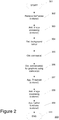
- FIG. 2 schematically illustrates a flow-chart of one embodiment of a thin-film material identification method. Shown is a flow-chart 300 that starts at step 301. Before or when starting, a digital image (e.g. like the one shown in Figure 1 ) is provided or obtained for automatic processing in order to identify single-, bi-, tri-, four- and/or few-layer thin-film material. In the following, graphene on a SiO 2 substrate will be used as an example.
- step 302 high-frequency noise - also often referred to as salt-and-pepper noise - is removed in order to obtain a more uniform digital image enabling more reliable detection of one or more regions comprising graphene.
- This may e.g. be done by applying a median filter or similar that replaces each pixel value with a median value of the surrounding pixels thereby effectively removing outlying pixels.
- a median filter is very effective at removing salt-and-pepper noise while preserving the sharpness of edges and therefore particular useful for enabling or improving precision of area identification and/or of subsequent edge detection if used (see below for step 309) and/or other functions.
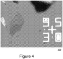
- FIG. 4 shows a digital image 100 after a median filter has been applied to the image of Figure 1 .
- Salt-and-pepper/high-frequency noise has been removed or diminished and the image contains more uniform colours.
- step 303 is carried out that applies additional image processing to enhance the identification process even further. More particularly, one or more dilation steps or similar is carried out followed by one or more erosion steps or similar. The number of dilation steps need not be equal to the number of erosion steps.
- Dilation and its counterpart - erosion - are in their basic form operations in mathematical morphology.
- Dilation is a convolution of a given image (binary, grey scale, or colour) with a kernel or the like, usually called a local maximum operator.
- the operation replaces all pixels with the maximum value of the surrounding pixels limited by the size and shape of the kernel.
- a square 3x3 pixel kernel may be used. This has e.g. been used in connection with Figures 5a - 5f but it is to be understood that other shapes and/or sizes of the kernel may be used.
- dilation may be used to remove edges around small pieces, spots, or areas of graphite and residues since pixels with a positive pixel contrast (i.e. darker than the background colour) close to the background colour will be eliminated.
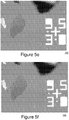
- Figures 5a - 5c illustrate one example of dilation being applied successively a number of times (in this particular example three times) to the image of Figure 4 .
- the part(s) of the image that corresponds to graphene is reduced in size as well during this process. Therefore, to more accurately obtain more exact boundaries or borders of areas of graphene, one or more applications of erosion is performed afterwards.
- Figures 5d - 5f shows one example of erosion being applied successively a number of times (in this particular example also three times).
- step 304 is carried out where the actual colour of the specific background, i.e. the actual colour of the specific substrate, is determined.
- the background colour changes over the entire, e.g. 4", wafer.
- the difference is quite pronounced and may be caused by small variations in the thickness of the substrate, the lamp intensity of an illuminating source, the microscope/image capturing device shutter time, and/or the defocus due to wafer bow, etc.
- the background colour is determined individually for each image to be processed for identification, e.g. as part of analysis of a series of images, to provide an actual colour of the specific background.
- the background colour may be determined once and used for subsequent images, which is simpler but not as accurate.
- One simple and efficient way to determine the background colour is simply to use predetermined information of an approximate range of a background colour for a given substrate of a given thickness.
- This predetermined information for one or more types of substrates may e.g. be stored physically in an appropriate electric memory and/or storage (see e.g. 203 in Figure 11 ) for retrieval or use when needed.
- the colour component value of each primary colour components R(ed), G(reen), and B(lue) is known to e.g. be about 175 ⁇ 10, 145 ⁇ 10, 140 ⁇ 10 .
- the single colour component value is known to be about 150 ⁇ 10. It is to be understood, that other intervals may be used instead, e.g. 140 ⁇ 5, 140 ⁇ 15, etc. for each primary colour.
- the range should not be too narrow (potentially discarding background pixels) or too broad (less of an issue with respect to loosing useful information but then simply wasting processing time and/or effort).
- RGB Red, Green, Blue
- HSL hue, saturation, luminance
- HSV hue, saturation, value
- HIS hue, saturation, and intensity
- the actual background colour component values (or grey-scale value) for the specific image may be determined, e.g. by determining a global optimum within the predetermined range for each colour component (or grey-scale value) assuming that the background colour will be the far more dominant colour of the image. This assumption is very safe to make for images of this kind with material located in this manner on a substrate. Alternatively, other methods for determining the background colour could be equally valid.
- the inventors have realised and shown that the contrast of graphene of a given type (i.e. being either single, bi-, tri-, four-, or few layer graphene) in a digital image - for a given thickness of the substrate that the graphene is deposited on - is constant (to within a small tolerance) - even for different colour spaces/models - and likewise that the contrast of graphene for each colour component is constant (to within a small tolerance) and uniquely determined by the substrate (and its thickness).
- a given type i.e. being either single, bi-, tri-, four-, or few layer graphene
- the contrast of graphene of a given layer is distinguishably different from the contrast of graphene of another given layer, e.g. the contrast of single layer graphene is different than the contrast of bi-layer graphene that is different than the contrast of tri-layer graphene, and so on.
- the contrast of bi-layer graphene is about 2 times the contrast of single-layer graphene, while the contrast of three-layer graphene is about 3 times the contrast of single-layer graphene, etc.
- the R, G, B contrasts [C R ; C G ; C B ] for a digital colour image of single-layer graphene on a 90 nm SiO 2 substrate is about [9%; 11%; 8%]. It can vary a bit due to small variations and errors.
- the inventors have for example experimentally measured contrasts to be e.g. about [8.6%; 10.5%; 8.1%] as well as other examples.
- Contrast values may simply be measured once for a given substrate as a function of the type of substrate and its thickness and then stored in a suitable memory and/or storage (see e.g. 203 in Figure 11 ) for later use.
- One way of determining the contrast values for a given substrate with a given thickness is e.g. to manually find a piece of graphene with an optical microscope, capture an image of the piece and measure the contrast.
- the specific value for each colour component of a given-layer graphene may then be determined using such predetermined contrast values [C R ; C G ; C B ] for each colour component and the determined background colour (as determined at step 304) also for each component.
- step 306 This is done at step 306 where the identified background colour components, each is multiplied by the result of 1 minus the contrast of the same colour component of the graphene in question (or the absolute value of the contrast of the same colour component of the graphene in question minus 1). It is to be understood that using values close to 1 may still give usable results. The preferred degree of how close to 1 the value should be may depend on actual application. Examples of a value to use instead of exactly 1 - e.g. depending on actual application - are e.g. values from 0.95 to 1.00; values from 0.90 to 1.00; values from 1.00 to 1.05; values from 1.00 to 1.10 with e.g.
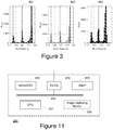
- the result will be 175 x (1 - 9%) being equal to about 159 signifying that single-layer graphene's red colour component has a value of about 159 in the actual image. This corresponds to the peak in pixel values seen in the red histogram around 159 in Figure 3 . In a similar way, the values for green and blue are determined.
- the actual (or a very good estimate thereof) colour of the given type of graphene with the given number of layers in the given image is determined. Areas or regions containing that particular type of graphene with that particular number of layers (being at least one) may then easily be identified e.g. simply by finding the parts of the image that have the same colour component values - preferably within a given range. This may e.g. be done simply searching for pixels in the image having the corresponding values (e.g. within a certain range) for each colour component.
- the single-layer graphene's red colour component has a value of 159 then all pixels having a red colour value within the range of e.g. 159 ⁇ 5 (and also fulfilling having a value within the suitable range for both green and blue) is determined to contain single-layer graphene.
- pixels may be determined according to (optional) steps 307 and 308 as will be described in the following.
- a threshold is applied at step 307, where all pixels are discarded (e.g. set to the colour black) except those pixels having values corresponding to a suitable relatively small range around values of the particular type of graphene.
- the remaining pixels may then be set to another colour, e.g. white.
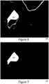
- An exemplary result of this may be seen in Figure 6 for single-layer graphene.
- the process may still be used on grey-scale image - but then with less precision - whereby the threshold is applied only for a single grey-scale colour.
- graphene may each be given their unique colour, e.g. single-layer graphene may be set to white, bi-layer graphene may be set to one given shade of grey, etc.
- Figure 8 shows an example of bi-layer graphene.
- the obtained threshold image may still contain some artefacts and noise - as also can be seen in Figures 6 and 8 .
- This may be removed, e.g. according to (optional) step 308, where one or more steps of erosion followed by one or more steps of dilation is performed.
- Figures 7 and 9 show the images of Figures 6 and 8 , respectively, after application of erosion followed by dilation and an area of graphene can clearly be seen and has been efficiently identified as such.
- step 309 further functions may (optionally) be applied as in step 309 depending on the use thereof.
- These functions may e.g. comprise applying an appropriate edge-or contour detection algorithm, e.g. enabling more quantitative information about a given area of graphene to be derived.
- Such parameters may be useful in characterising the graphene areas.
- Especially area and circularity may be important parameters or constraints for detection of suitable graphene areas e.g. for use to be post-processed with E-beam lithography for Hall-bar devices requiring a certain length and width or for other uses.
- a location of a graphene area on the substrate or wafer may be determined using the index marks of the image.
- This location information may e.g. (together with other relevant parameters) be used in a CAD program or similar enabling automatic optimised placement of devices in the identified graphene areas. This could include the identification of position and/or orientation of individual domains of graphene grown on Cu, Ni, SiC, Ru, Ir and similar materials before or after transfer processes and processing.
- Figure 10 shows the end result of processing the image of Figure 1 showing both identified single- and bi-layer graphene.
- the method may loop back to step 301 or 302 and process another image if applicable. This may e.g. be continued until all images of a wafer or similar has been processed and can also continue for more wafers.
- steps 304 and 305 e.g. may be switched or even done in parallel.
- step 302 may be done after step 303.
- Figure 3 schematically illustrates a graph of pixel histograms of each colour component obtained for an area around the single- and bi-layer graphene in Figure 1 to make the information more clear. Alternatively, they may be derived for the entire image. Shown is a pixel histogram for each of the colour components R (401), G (402), and B (403). The rightmost dashed line is for the background colour, the middle dashed line is for single-layer graphene, while the left dashed line is for bi-layer graphene.
- Figure 4 schematically illustrates the image of Figure 1 after (optional) image processing removing so-called salt-and-pepper noise without blurring edges in the image. Shown is a processed digital image 100.
- Figures 5a - 5f schematically illustrate the effect of (optional) additional image processing of the image of Figure 1 .
- Figures 5a - 5c illustrate the effect of applying dilation three times (one application per Figure).
- Figures 5d - 5f illustrate the effect of applying erosion three times (one application per Figure).
- Figure 6 schematically illustrates the image of Figure 1 after single-layer graphene has been identified and non-graphene has been removed with some artefacts and noise still present.
- Figure 7 schematically illustrates Figure 6 after some additional image processing removing noise and/or artefacts.
- Figure 8 schematically illustrates the image of Figure 1 after bi-layer graphene has been identified and non-graphene has been removed.
- Figure 9 schematically illustrates Figure 8 after some additional image processing removing noise and/or artefacts.
- Figure 10 schematically illustrates the end result of processing the image of Figure 1 showing both identified single- and bi-layer graphene.
- FIG 11 schematically illustrates one embodiment of a system for automatic identification of a digital representation of single-, bi-, and/or few-layer thin-film material, e.g. graphene, in a digital image.
- a system 200 comprising at least one processing unit 201 connected via one or more communications and/or data buses 202 to a memory and/or storage 203, optional communications elements 204 e.g. for communicating via a network, the Internet, a Wi-Fi connection, and/or the like, and an (optional) display 205.
- the system 200 may be a more or less standard computational system, like a PC, laptop, tablet, etc. or any other appropriate system suitably programmed to carry out the method or procedure as described in the various embodiments throughout the specification and variations thereof.
- the system 200 optionally also comprises an image capturing device 206 for obtaining images like the one shown in Figure 1 . Alternatively, such an image may simply be provided to the system 200.
- any reference signs placed between parentheses shall not be constructed as limiting the claim.
- the word “comprising” does not exclude the presence of elements or steps other than those listed in a claim.
- the word “a” or “an” preceding an element does not exclude the presence of a plurality of such elements.
Landscapes
- Engineering & Computer Science (AREA)
- Computer Vision & Pattern Recognition (AREA)
- Physics & Mathematics (AREA)
- General Physics & Mathematics (AREA)
- Theoretical Computer Science (AREA)
- Image Analysis (AREA)
Claims (14)
- Procédé destiné à identifier automatiquement une ou plusieurs représentations numériques d'un matériau à une seule couche mince (101) et/ou à un petit nombre de couches minces (102) dans une image numérique (100), l'image numérique (100) possédant un nombre prédéterminé de composantes de couleur, le procédé comprenant- la détermination (304) d'une composante de couleur d'arrière-plan de l'image numérique (100) pour chaque composante de couleur, et- la détermination ou l'estimation (306) d'une composante de couleur d'un matériau à couche mince à identifier dans l'image numérique (100) pour chaque composante de couleur, le matériau à couche mince à identifier possédant un nombre donné de couches supérieur ou égal à un,ladite détermination ou ladite estimation (306) d'une composante de couleur d'un matériau à couche mince à identifier dans l'image numérique (100) pour chaque composante de couleur comprenant- l'obtention d'une valeur de contraste prédéterminée pour chaque composante de couleur et la détermination ou l'estimation de la composante de couleur du matériau à couche mince à identifier et l'obtention du nombre de couches donné pour chaque composante de couleur en multipliant, pour chaque composante de couleur, la différence numérique entre la valeur de contraste prédéterminée pour une composante de couleur donnée et environ 1 par la composante de couleur d'arrière-plan pour la composante de couleur donnée,et ledit procédé comprenant en outre- l'identification (307) d'une ou plusieurs représentations numériques d'un matériau à une seule couche mince (101) et/ou à un petit nombre de couches minces (102) sous forme de points ou de parties de l'image numérique (100) qui, pour chaque composante de couleur, possède une composante de couleur comprise à l'intérieur d'une plage prédéterminée de composantes de couleur déterminées ou estimées du matériau à couche mince à identifier possédant ledit nombre de couches donné,caractérisé en ce que ladite valeur de contraste prédéterminée obtenue pour chaque composante de couleur a été déduite de :- la différence numérique entre l'intensité de couleur de l'arrière-plan de la composante de couleur donnée et l'intensité de couleur du matériau à couche mince à identifier de la composante de couleur donnée divisée par l'intensité de couleur de l'arrière-plan de la composante de couleur donnée.
- Procédé selon la revendication 1, ledit matériau à couche mince étant du graphène.
- Procédé selon le revendication 1, ledit matériau à couche mince étant l'un quelconque sélectionné dans le groupe comprenant :- le disulfure de molybdène,- le nitrure de bore hexagonal,- Sb2Te3,- MoTe2,- WS2,- MoSe2,- TaSe2,- Bi2Te3,- NbSe2, et- NiTe2.
- Procédé selon l'une quelconque des revendications 1 à 3,- ladite image numérique (100) étant une image en échelle de gris ou étant convertie en une image en échelle de gris et le nombre de composantes de couleur étant égal à un, ou- ladite image numérique (100) étant une image en couleur et le nombre de composantes de couleur étant de trois ou plus.
- Procédé selon l'une quelconque des revendications 1 à 4, ledit procédé comprenant l'identification d'une ou plusieurs représentations numériques d'un matériau à une seule couche mince (101) et/ou à un petit nombre de couches minces (102) dans une série d'images numériques (100),- ladite détermination (304) d'une composante de couleur d'arrière-plan de l'image numérique (100) pour chaque composante de couleur, et/ou- ladite détermination ou ladite estimation (306) d'une composante de couleur du matériau à couche mince à identifier dans l'image numérique (100) pour chaque composante de couleur,étant réalisées pour chaque image numérique de la série ou étant réalisées une fois lorsque la détermination ou les déterminations sont utilisées pour les images numériques ultérieures de la série.
- Procédé selon l'une quelconque des revendications 1 à 5, ledit matériau à couche mince de l'image numérique (100) s'étant trouvé sur un substrat donné, possédant une épaisseur prédéterminée, lors de la capture de l'image numérique et ladite détermination (304) d'une composante de couleur d'arrière-plan de l'image numérique (100) pour chaque composante de couleur comprenant- l'apport d'informations prédéterminées d'une plage approximative de composantes de couleur d'arrière-plan pour chaque composante de couleur en fonction de l'épaisseur et du type particulier du substrat donné.
- Procédé selon l'une quelconque des revendications 1 à 6, ledit procédé comprenant en outre :- l'application d'un filtre (302), e.g. un filtre médian, à l'image numérique (100) pour éliminer le bruit haute fréquence et/ou le bruit poivre et sel avant la détermination (304) de la composante de couleur d'arrière-plan de l'image numérique (100) pour chaque composante de couleur,- l'application (303) d'une ou plusieurs étapes de dilatation suivies par une ou plusieurs étapes d'érosion dans le but d'améliorer la qualité de l'image numérique (100) pour l'identification du matériau à couche mince,- l'application d'un seuil (307), où tous les pixels de l'image numérique (100) sont supprimés à l'exception des pixels qui possèdent, pour chaque composante de couleur, une composante de couleur comprise dans une seconde plage prédéterminée de la composante de couleur déterminée ou estimée du matériau à couche mince à identifier possédant le nombre de couches donné, et/ou- la détection des bords ou du contour (309) d'au moins une partie de l'image numérique (100) qui a été identifiée comme étant une ou plusieurs représentations numériques du matériau à une seule couche mince (101) et/ou à un petit nombre de couches minces (102).
- Système (200) pour l'identification automatique d'une ou plusieurs représentations numériques d'un matériau à une seule couche mince (101) et/ou à un petit nombre de couches minces (102) dans une image numérique (100), l'image numérique (100) possédant un nombre prédéterminé de composantes de couleur, ledit système comprenant une ou plusieurs unités de traitement (201) adaptées pour- déterminer la composante de couleur d'arrière-plan de l'image numérique (100) pour chaque composante de couleur, et- déterminer ou estimer une composante de couleur d'un matériau à couche mince à identifier dans l'image numérique (100) pour chaque composante de couleur, le matériau à couche mince à identifier possédant un nombre de couches donné supérieur ou égal à un,une ou plusieurs desdites unités de traitement (201) étant adaptées pour déterminer ou estimer une composante de couleur d'un matériau à couche mince à identifier dans l'image numérique (100) pour chaque composante de couleur par- l'obtention d'une valeur de contraste prédéterminée pour chaque composante de couleur et la détermination ou l'estimation de la composante de couleur du matériau à couche mince à identifier et l'obtention du nombre de couches donné pour chaque composante de couleur en multipliant, pour chaque composante de couleur, la différence numérique entre la valeur de contraste prédéterminée pour une composante de couleur donnée et environ 1 par la composante de couleur d'arrière-plan pour la composante de couleur donnée,lesdites une ou plusieurs unités de traitement (201) étant adaptées en outre pour- identifier une ou plusieurs représentations numériques du matériau à une seule couche mince (101) et/ou à un petit nombre de couches minces (102) sous forme de points ou de parties de l'image numérique (100) qui, pour chaque composante de couleur, possède une composante de couleur comprise dans une plage prédéterminée de composantes de couleur déterminées ou estimées du matériau à couche mince à identifier possédant le nombre de couches donné, etcaractérisé en ce que ladite valeur de contraste prédéterminée obtenue pour chaque composante de couleur a été déduite de :- la différence numérique entre l'intensité de couleur de l'arrière-plan de la composante de couleur donnée et l'intensité de couleur du matériau à couche mince à identifier de la composante de couleur donnée divisée par l'intensité de couleur de l'arrière-plan de la composante de couleur donnée.
- Système selon la revendication 8, ledit matériau à couche mince étant du graphène.
- Système selon la revendication 8, ledit matériau à couche mince étant l'un quelconque sélectionné dans le groupe comprenant- le disulfure de molybdène,- le nitrure de bore hexagonal,- Sb2Te3,- MoTe2,- WS2,- MoSe2,- TaSe2,- Bi2Te3,- NbSe2, et- NiTe2.
- Système selon l'une quelconque des revendications 8 à 10,- ladite image numérique (100) étant une image en échelle de gris ou étant convertie en une image en échelle de gris et le nombre de composantes de couleur étant égal à un, ou- ladite image numérique (100) étant une image en couleur et le nombre de composantes de couleur étant de trois ou plus.
- Système selon l'une quelconque des revendications 8 à 11, ledit système étant adapté pour identifier une ou plusieurs représentations numériques d'un matériau à une seule couche mince (101) et/ou à un petit nombre de couches minces (102) dans une série d'images numériques (100),- ladite détermination de la composante de couleur d'arrière-plan de l'image numérique (100) pour chaque composante de couleur, et/ou- ladite détermination ou ladite estimation de la composante de couleur du matériau à couche mince à identifier dans l'image numérique (100) pour chaque composante de couleur,étant réalisées pour chaque image numérique de la série ou étant réalisées une fois lorsque la détermination ou les déterminations sont utilisées pour les images numériques ultérieures de la série.
- Système selon l'une quelconque des revendications 8 à 12, ledit matériau à couche mince de l'image numérique (100) s'étant trouvé sur un substrat donné, possédant une épaisseur prédéterminée, lors de la capture de l'image numérique et lesdites une ou plusieurs unités de traitement (201) étant adaptées pour déterminer une composante de couleur d'arrière-plan de l'image numérique (100) pour chaque composante de couleur par- l'apport d'informations prédéterminées d'une plage approximative de composantes de couleur d'arrière-plan pour chaque composante de couleur en fonction de l'épaisseur et du type particulier du substrat donné.
- Système selon l'une quelconque des revendications 8 à 13, lesdites une ou plusieurs unités de traitement (201) étant adaptées en outre à- l'application d'un filtre, e.g. un filtre médian, à une image numérique (100) pour éliminer le bruit haute fréquence et/ou le bruit poivre et sel avant la détermination d'une composante de couleur d'arrière-plan de l'image numérique (100) pour chaque composante de couleur,- l'application d'une ou plusieurs étapes de dilatation suivies d'une ou plusieurs étapes d'érosion dans le but d'améliorer la qualité de l'image numérique (100) pour l'identification du matériau à couche mince,- l'application d'un seuil où tous les pixels de l'image numérique (100) sont supprimés à l'exception des pixels qui possèdent pour chaque composante de couleur, une composante de couleur comprise dans une seconde plage prédéterminée de composantes de couleur déterminées ou estimées du matériau à couche mince à identifier possédant le nombre de couches donné, et/ou- la détection des bords ou du contour d'au moins une partie de l'image numérique (100) qui a été identifiée comme étant une ou plusieurs représentations numériques d'un matériau à une seule couche mince (101) et/ou à un petit nombre de couches minces (102).
Priority Applications (1)
| Application Number | Priority Date | Filing Date | Title |
|---|---|---|---|
| EP13755943.1A EP2883207B8 (fr) | 2012-08-13 | 2013-08-13 | Identification automatique de matériaux à couche mince en quelques couches et/ou mono-couche |
Applications Claiming Priority (3)
| Application Number | Priority Date | Filing Date | Title |
|---|---|---|---|
| EP12180234 | 2012-08-13 | ||
| EP13755943.1A EP2883207B8 (fr) | 2012-08-13 | 2013-08-13 | Identification automatique de matériaux à couche mince en quelques couches et/ou mono-couche |
| PCT/DK2013/050264 WO2014026692A1 (fr) | 2012-08-13 | 2013-08-13 | Identification automatique de matériau à une seule couche mince et/ou à un petit nombre de couches minces seulement |
Publications (3)
| Publication Number | Publication Date |
|---|---|
| EP2883207A1 EP2883207A1 (fr) | 2015-06-17 |
| EP2883207B1 true EP2883207B1 (fr) | 2017-05-10 |
| EP2883207B8 EP2883207B8 (fr) | 2017-08-02 |
Family
ID=47002592
Family Applications (1)
| Application Number | Title | Priority Date | Filing Date |
|---|---|---|---|
| EP13755943.1A Not-in-force EP2883207B8 (fr) | 2012-08-13 | 2013-08-13 | Identification automatique de matériaux à couche mince en quelques couches et/ou mono-couche |
Country Status (6)
| Country | Link |
|---|---|
| US (1) | US9251601B2 (fr) |
| EP (1) | EP2883207B8 (fr) |
| KR (1) | KR20150045464A (fr) |
| CN (1) | CN104737201A (fr) |
| ES (1) | ES2642350T3 (fr) |
| WO (1) | WO2014026692A1 (fr) |
Families Citing this family (3)
| Publication number | Priority date | Publication date | Assignee | Title |
|---|---|---|---|---|
| WO2018005431A1 (fr) * | 2016-06-27 | 2018-01-04 | The Regents Of The University Of California | Procédé de visualisation optique directe de graphène et de ses défauts à l'échelle nanométrique sur des substrats transparents |
| US20200160089A1 (en) * | 2018-11-15 | 2020-05-21 | International Business Machines Corporation | Visual pattern recognition with selective illumination for assisted inspection |
| CN113574857B (zh) * | 2019-03-25 | 2023-10-31 | 日本电气株式会社 | 图像处理设备和图像处理方法 |
Family Cites Families (6)
| Publication number | Priority date | Publication date | Assignee | Title |
|---|---|---|---|---|
| US6236459B1 (en) * | 1998-11-05 | 2001-05-22 | University Of Miami | Thin film measuring device and method |
| US7522762B2 (en) | 2003-04-16 | 2009-04-21 | Inverness Medical-Biostar, Inc. | Detection, resolution, and identification of arrayed elements |
| WO2009094277A2 (fr) | 2008-01-14 | 2009-07-30 | The Regents Of The University Of California | Traitement en solution à capacité élevée de graphène à grande échelle et applications de dispositifs |
| JP5142278B2 (ja) * | 2008-08-14 | 2013-02-13 | 独立行政法人産業技術総合研究所 | グラフェン又は超薄膜グラファイトの厚さ検出方法および厚さ検出システム |
| US8426120B2 (en) | 2009-09-29 | 2013-04-23 | Northwestern University | High-throughput imaging of graphene based sheets by fluorescence quenching microscopy and applications of same |
| US20110299720A1 (en) | 2010-03-18 | 2011-12-08 | The Regents Of The University Of California | Systems and methods for material layer identification through image processing |
-
2013
- 2013-08-13 EP EP13755943.1A patent/EP2883207B8/fr not_active Not-in-force
- 2013-08-13 WO PCT/DK2013/050264 patent/WO2014026692A1/fr not_active Ceased
- 2013-08-13 ES ES13755943.1T patent/ES2642350T3/es active Active
- 2013-08-13 CN CN201380053502.4A patent/CN104737201A/zh active Pending
- 2013-08-13 US US14/419,869 patent/US9251601B2/en not_active Expired - Fee Related
- 2013-08-13 KR KR1020157006430A patent/KR20150045464A/ko not_active Ceased
Also Published As
| Publication number | Publication date |
|---|---|
| CN104737201A (zh) | 2015-06-24 |
| KR20150045464A (ko) | 2015-04-28 |
| ES2642350T3 (es) | 2017-11-16 |
| US9251601B2 (en) | 2016-02-02 |
| EP2883207A1 (fr) | 2015-06-17 |
| US20150199826A1 (en) | 2015-07-16 |
| EP2883207B8 (fr) | 2017-08-02 |
| WO2014026692A1 (fr) | 2014-02-20 |
Similar Documents
| Publication | Publication Date | Title |
|---|---|---|
| JP4006007B2 (ja) | ひび割れ検出方法 | |
| TWI716684B (zh) | 臨界尺寸量測方法及用於量測臨界尺寸的影像處理裝置 | |
| CN109685760B (zh) | 一种基于matlab的slm粉床铺粉图像凸包凹陷缺陷检测方法 | |
| JP5385593B2 (ja) | ひび割れ検出方法 | |
| EP1821065A1 (fr) | Procédé de mesure de déformation de la surface arrière d'un substrat | |
| CN114565552B (zh) | 光学元件表面缺陷的检测方法、装置及电子设备 | |
| JP5705711B2 (ja) | ひび割れ検出方法 | |
| US12207935B2 (en) | Quantitative image-based disorder analysis for early detection of melanoma type features | |
| JP4870016B2 (ja) | ひび割れ検出方法 | |
| EP2883207B1 (fr) | Identification automatique de matériaux à couche mince en quelques couches et/ou mono-couche | |
| CN112561905A (zh) | 有图形晶圆的图像优化方法、复检方法和复检设备 | |
| CN114166171A (zh) | 晶体缺陷的检测方法与检测装置 | |
| JP3844973B2 (ja) | 基板の研磨終点検出 | |
| CN1329951C (zh) | 对齐晶片的方法 | |
| EP2876602A1 (fr) | Procédé et dispositif d'analyse d'images de réseau de nanostructures | |
| JP6637823B2 (ja) | ひび割れ検出方法 | |
| CN108280825A (zh) | 一种液晶显示屏边缘缺口检测方法 | |
| JP6666171B2 (ja) | 欠陥検査装置 | |
| Shi et al. | Automatic recognition and evaluation of micro-contaminant particles on ultra-smooth optical substrates using image analysis method | |
| CN110689926A (zh) | 一种高通量数字pcr图像液滴的准确检测方法 | |
| CN115272326A (zh) | 一种电子元器件表面裂痕的检测方法 | |
| CN114972227A (zh) | 一种砂轮气孔率测定方法 | |
| JP2005315748A (ja) | データ圧縮方法、欠陥検査方法および欠陥検査装置 | |
| JP3787547B2 (ja) | 結晶欠陥の自動検査方法及び自動検査装置 | |
| Yang et al. | Research on automatic dodging method for road surface line array images |
Legal Events
| Date | Code | Title | Description |
|---|---|---|---|
| PUAI | Public reference made under article 153(3) epc to a published international application that has entered the european phase |
Free format text: ORIGINAL CODE: 0009012 |
|
| 17P | Request for examination filed |
Effective date: 20150223 |
|
| AK | Designated contracting states |
Kind code of ref document: A1 Designated state(s): AL AT BE BG CH CY CZ DE DK EE ES FI FR GB GR HR HU IE IS IT LI LT LU LV MC MK MT NL NO PL PT RO RS SE SI SK SM TR |
|
| AX | Request for extension of the european patent |
Extension state: BA ME |
|
| DAX | Request for extension of the european patent (deleted) | ||
| 17Q | First examination report despatched |
Effective date: 20160322 |
|
| GRAP | Despatch of communication of intention to grant a patent |
Free format text: ORIGINAL CODE: EPIDOSNIGR1 |
|
| STAA | Information on the status of an ep patent application or granted ep patent |
Free format text: STATUS: GRANT OF PATENT IS INTENDED |
|
| INTG | Intention to grant announced |
Effective date: 20161125 |
|
| GRAS | Grant fee paid |
Free format text: ORIGINAL CODE: EPIDOSNIGR3 |
|
| GRAA | (expected) grant |
Free format text: ORIGINAL CODE: 0009210 |
|
| STAA | Information on the status of an ep patent application or granted ep patent |
Free format text: STATUS: THE PATENT HAS BEEN GRANTED |
|
| RAP1 | Party data changed (applicant data changed or rights of an application transferred) |
Owner name: DANMARKS TEKNISKE UNIVERSITET (DTU) |
|
| AK | Designated contracting states |
Kind code of ref document: B1 Designated state(s): AL AT BE BG CH CY CZ DE DK EE ES FI FR GB GR HR HU IE IS IT LI LT LU LV MC MK MT NL NO PL PT RO RS SE SI SK SM TR |
|
| REG | Reference to a national code |
Ref country code: GB Ref legal event code: FG4D |
|
| REG | Reference to a national code |
Ref country code: AT Ref legal event code: REF Ref document number: 893060 Country of ref document: AT Kind code of ref document: T Effective date: 20170515 Ref country code: CH Ref legal event code: EP |
|
| GRAT | Correction requested after decision to grant or after decision to maintain patent in amended form |
Free format text: ORIGINAL CODE: EPIDOSNCDEC |
|
| RAP2 | Party data changed (patent owner data changed or rights of a patent transferred) |
Owner name: DANMARKS TEKNISKE UNIVERSITET |
|
| REG | Reference to a national code |
Ref country code: IE Ref legal event code: FG4D |
|
| REG | Reference to a national code |
Ref country code: DE Ref legal event code: R096 Ref document number: 602013020971 Country of ref document: DE |
|
| REG | Reference to a national code |
Ref country code: NL Ref legal event code: MP Effective date: 20170510 |
|
| REG | Reference to a national code |
Ref country code: LT Ref legal event code: MG4D |
|
| REG | Reference to a national code |
Ref country code: AT Ref legal event code: MK05 Ref document number: 893060 Country of ref document: AT Kind code of ref document: T Effective date: 20170510 |
|
| PG25 | Lapsed in a contracting state [announced via postgrant information from national office to epo] |
Ref country code: LT Free format text: LAPSE BECAUSE OF FAILURE TO SUBMIT A TRANSLATION OF THE DESCRIPTION OR TO PAY THE FEE WITHIN THE PRESCRIBED TIME-LIMIT Effective date: 20170510 Ref country code: HR Free format text: LAPSE BECAUSE OF FAILURE TO SUBMIT A TRANSLATION OF THE DESCRIPTION OR TO PAY THE FEE WITHIN THE PRESCRIBED TIME-LIMIT Effective date: 20170510 Ref country code: GR Free format text: LAPSE BECAUSE OF FAILURE TO SUBMIT A TRANSLATION OF THE DESCRIPTION OR TO PAY THE FEE WITHIN THE PRESCRIBED TIME-LIMIT Effective date: 20170811 Ref country code: AT Free format text: LAPSE BECAUSE OF FAILURE TO SUBMIT A TRANSLATION OF THE DESCRIPTION OR TO PAY THE FEE WITHIN THE PRESCRIBED TIME-LIMIT Effective date: 20170510 Ref country code: NO Free format text: LAPSE BECAUSE OF FAILURE TO SUBMIT A TRANSLATION OF THE DESCRIPTION OR TO PAY THE FEE WITHIN THE PRESCRIBED TIME-LIMIT Effective date: 20170810 Ref country code: FI Free format text: LAPSE BECAUSE OF FAILURE TO SUBMIT A TRANSLATION OF THE DESCRIPTION OR TO PAY THE FEE WITHIN THE PRESCRIBED TIME-LIMIT Effective date: 20170510 |
|
| REG | Reference to a national code |
Ref country code: ES Ref legal event code: FG2A Ref document number: 2642350 Country of ref document: ES Kind code of ref document: T3 Effective date: 20171116 |
|
| PG25 | Lapsed in a contracting state [announced via postgrant information from national office to epo] |
Ref country code: NL Free format text: LAPSE BECAUSE OF FAILURE TO SUBMIT A TRANSLATION OF THE DESCRIPTION OR TO PAY THE FEE WITHIN THE PRESCRIBED TIME-LIMIT Effective date: 20170510 Ref country code: IS Free format text: LAPSE BECAUSE OF FAILURE TO SUBMIT A TRANSLATION OF THE DESCRIPTION OR TO PAY THE FEE WITHIN THE PRESCRIBED TIME-LIMIT Effective date: 20170910 Ref country code: LV Free format text: LAPSE BECAUSE OF FAILURE TO SUBMIT A TRANSLATION OF THE DESCRIPTION OR TO PAY THE FEE WITHIN THE PRESCRIBED TIME-LIMIT Effective date: 20170510 Ref country code: SE Free format text: LAPSE BECAUSE OF FAILURE TO SUBMIT A TRANSLATION OF THE DESCRIPTION OR TO PAY THE FEE WITHIN THE PRESCRIBED TIME-LIMIT Effective date: 20170510 Ref country code: BG Free format text: LAPSE BECAUSE OF FAILURE TO SUBMIT A TRANSLATION OF THE DESCRIPTION OR TO PAY THE FEE WITHIN THE PRESCRIBED TIME-LIMIT Effective date: 20170810 Ref country code: PL Free format text: LAPSE BECAUSE OF FAILURE TO SUBMIT A TRANSLATION OF THE DESCRIPTION OR TO PAY THE FEE WITHIN THE PRESCRIBED TIME-LIMIT Effective date: 20170510 Ref country code: RS Free format text: LAPSE BECAUSE OF FAILURE TO SUBMIT A TRANSLATION OF THE DESCRIPTION OR TO PAY THE FEE WITHIN THE PRESCRIBED TIME-LIMIT Effective date: 20170510 |
|
| PG25 | Lapsed in a contracting state [announced via postgrant information from national office to epo] |
Ref country code: EE Free format text: LAPSE BECAUSE OF FAILURE TO SUBMIT A TRANSLATION OF THE DESCRIPTION OR TO PAY THE FEE WITHIN THE PRESCRIBED TIME-LIMIT Effective date: 20170510 Ref country code: CZ Free format text: LAPSE BECAUSE OF FAILURE TO SUBMIT A TRANSLATION OF THE DESCRIPTION OR TO PAY THE FEE WITHIN THE PRESCRIBED TIME-LIMIT Effective date: 20170510 Ref country code: DK Free format text: LAPSE BECAUSE OF FAILURE TO SUBMIT A TRANSLATION OF THE DESCRIPTION OR TO PAY THE FEE WITHIN THE PRESCRIBED TIME-LIMIT Effective date: 20170510 Ref country code: SK Free format text: LAPSE BECAUSE OF FAILURE TO SUBMIT A TRANSLATION OF THE DESCRIPTION OR TO PAY THE FEE WITHIN THE PRESCRIBED TIME-LIMIT Effective date: 20170510 Ref country code: RO Free format text: LAPSE BECAUSE OF FAILURE TO SUBMIT A TRANSLATION OF THE DESCRIPTION OR TO PAY THE FEE WITHIN THE PRESCRIBED TIME-LIMIT Effective date: 20170510 |
|
| REG | Reference to a national code |
Ref country code: DE Ref legal event code: R097 Ref document number: 602013020971 Country of ref document: DE |
|
| PG25 | Lapsed in a contracting state [announced via postgrant information from national office to epo] |
Ref country code: SM Free format text: LAPSE BECAUSE OF FAILURE TO SUBMIT A TRANSLATION OF THE DESCRIPTION OR TO PAY THE FEE WITHIN THE PRESCRIBED TIME-LIMIT Effective date: 20170510 Ref country code: IT Free format text: LAPSE BECAUSE OF FAILURE TO SUBMIT A TRANSLATION OF THE DESCRIPTION OR TO PAY THE FEE WITHIN THE PRESCRIBED TIME-LIMIT Effective date: 20170510 |
|
| PLBE | No opposition filed within time limit |
Free format text: ORIGINAL CODE: 0009261 |
|
| STAA | Information on the status of an ep patent application or granted ep patent |
Free format text: STATUS: NO OPPOSITION FILED WITHIN TIME LIMIT |
|
| REG | Reference to a national code |
Ref country code: CH Ref legal event code: PL |
|
| PG25 | Lapsed in a contracting state [announced via postgrant information from national office to epo] |
Ref country code: MC Free format text: LAPSE BECAUSE OF FAILURE TO SUBMIT A TRANSLATION OF THE DESCRIPTION OR TO PAY THE FEE WITHIN THE PRESCRIBED TIME-LIMIT Effective date: 20170510 |
|
| 26N | No opposition filed |
Effective date: 20180213 |
|
| PG25 | Lapsed in a contracting state [announced via postgrant information from national office to epo] |
Ref country code: CH Free format text: LAPSE BECAUSE OF NON-PAYMENT OF DUE FEES Effective date: 20170831 Ref country code: LI Free format text: LAPSE BECAUSE OF NON-PAYMENT OF DUE FEES Effective date: 20170831 |
|
| REG | Reference to a national code |
Ref country code: FR Ref legal event code: ST Effective date: 20180430 |
|
| REG | Reference to a national code |
Ref country code: IE Ref legal event code: MM4A |
|
| PG25 | Lapsed in a contracting state [announced via postgrant information from national office to epo] |
Ref country code: SI Free format text: LAPSE BECAUSE OF FAILURE TO SUBMIT A TRANSLATION OF THE DESCRIPTION OR TO PAY THE FEE WITHIN THE PRESCRIBED TIME-LIMIT Effective date: 20170510 |
|
| REG | Reference to a national code |
Ref country code: BE Ref legal event code: MM Effective date: 20170831 |
|
| PG25 | Lapsed in a contracting state [announced via postgrant information from national office to epo] |
Ref country code: LU Free format text: LAPSE BECAUSE OF NON-PAYMENT OF DUE FEES Effective date: 20170813 |
|
| PG25 | Lapsed in a contracting state [announced via postgrant information from national office to epo] |
Ref country code: IE Free format text: LAPSE BECAUSE OF NON-PAYMENT OF DUE FEES Effective date: 20170813 |
|
| PG25 | Lapsed in a contracting state [announced via postgrant information from national office to epo] |
Ref country code: FR Free format text: LAPSE BECAUSE OF NON-PAYMENT OF DUE FEES Effective date: 20170831 Ref country code: BE Free format text: LAPSE BECAUSE OF NON-PAYMENT OF DUE FEES Effective date: 20170831 |
|
| PG25 | Lapsed in a contracting state [announced via postgrant information from national office to epo] |
Ref country code: MT Free format text: LAPSE BECAUSE OF NON-PAYMENT OF DUE FEES Effective date: 20170813 |
|
| PGFP | Annual fee paid to national office [announced via postgrant information from national office to epo] |
Ref country code: ES Payment date: 20180921 Year of fee payment: 6 Ref country code: DE Payment date: 20180823 Year of fee payment: 6 |
|
| PGFP | Annual fee paid to national office [announced via postgrant information from national office to epo] |
Ref country code: GB Payment date: 20180822 Year of fee payment: 6 |
|
| PG25 | Lapsed in a contracting state [announced via postgrant information from national office to epo] |
Ref country code: HU Free format text: LAPSE BECAUSE OF FAILURE TO SUBMIT A TRANSLATION OF THE DESCRIPTION OR TO PAY THE FEE WITHIN THE PRESCRIBED TIME-LIMIT; INVALID AB INITIO Effective date: 20130813 |
|
| PG25 | Lapsed in a contracting state [announced via postgrant information from national office to epo] |
Ref country code: CY Free format text: LAPSE BECAUSE OF FAILURE TO SUBMIT A TRANSLATION OF THE DESCRIPTION OR TO PAY THE FEE WITHIN THE PRESCRIBED TIME-LIMIT Effective date: 20170510 |
|
| PG25 | Lapsed in a contracting state [announced via postgrant information from national office to epo] |
Ref country code: MK Free format text: LAPSE BECAUSE OF FAILURE TO SUBMIT A TRANSLATION OF THE DESCRIPTION OR TO PAY THE FEE WITHIN THE PRESCRIBED TIME-LIMIT Effective date: 20170510 |
|
| REG | Reference to a national code |
Ref country code: DE Ref legal event code: R119 Ref document number: 602013020971 Country of ref document: DE |
|
| PG25 | Lapsed in a contracting state [announced via postgrant information from national office to epo] |
Ref country code: TR Free format text: LAPSE BECAUSE OF FAILURE TO SUBMIT A TRANSLATION OF THE DESCRIPTION OR TO PAY THE FEE WITHIN THE PRESCRIBED TIME-LIMIT Effective date: 20170510 |
|
| GBPC | Gb: european patent ceased through non-payment of renewal fee |
Effective date: 20190813 |
|
| PG25 | Lapsed in a contracting state [announced via postgrant information from national office to epo] |
Ref country code: PT Free format text: LAPSE BECAUSE OF FAILURE TO SUBMIT A TRANSLATION OF THE DESCRIPTION OR TO PAY THE FEE WITHIN THE PRESCRIBED TIME-LIMIT Effective date: 20170510 |
|
| PG25 | Lapsed in a contracting state [announced via postgrant information from national office to epo] |
Ref country code: DE Free format text: LAPSE BECAUSE OF NON-PAYMENT OF DUE FEES Effective date: 20200303 Ref country code: AL Free format text: LAPSE BECAUSE OF FAILURE TO SUBMIT A TRANSLATION OF THE DESCRIPTION OR TO PAY THE FEE WITHIN THE PRESCRIBED TIME-LIMIT Effective date: 20170510 |
|
| PG25 | Lapsed in a contracting state [announced via postgrant information from national office to epo] |
Ref country code: GB Free format text: LAPSE BECAUSE OF NON-PAYMENT OF DUE FEES Effective date: 20190813 |
|
| REG | Reference to a national code |
Ref country code: ES Ref legal event code: FD2A Effective date: 20210105 |
|
| PG25 | Lapsed in a contracting state [announced via postgrant information from national office to epo] |
Ref country code: ES Free format text: LAPSE BECAUSE OF NON-PAYMENT OF DUE FEES Effective date: 20190814 |