EP2884666B1 - Dispositif FPGA avec interconnexion programmable dans une partie d'extrémité arrière de ligne du dispositif - Google Patents
Dispositif FPGA avec interconnexion programmable dans une partie d'extrémité arrière de ligne du dispositif Download PDFInfo
- Publication number
- EP2884666B1 EP2884666B1 EP14191906.8A EP14191906A EP2884666B1 EP 2884666 B1 EP2884666 B1 EP 2884666B1 EP 14191906 A EP14191906 A EP 14191906A EP 2884666 B1 EP2884666 B1 EP 2884666B1
- Authority
- EP
- European Patent Office
- Prior art keywords
- fpga
- layer
- transistor
- beol
- interconnect
- Prior art date
- Legal status (The legal status is an assumption and is not a legal conclusion. Google has not performed a legal analysis and makes no representation as to the accuracy of the status listed.)
- Active
Links
Images




Classifications
-
- H—ELECTRICITY
- H10—SEMICONDUCTOR DEVICES; ELECTRIC SOLID-STATE DEVICES NOT OTHERWISE PROVIDED FOR
- H10P—GENERIC PROCESSES OR APPARATUS FOR THE MANUFACTURE OR TREATMENT OF DEVICES COVERED BY CLASS H10
- H10P95/00—Generic processes or apparatus for manufacture or treatments not covered by the other groups of this subclass
-
- H—ELECTRICITY
- H03—ELECTRONIC CIRCUITRY
- H03K—PULSE TECHNIQUE
- H03K19/00—Logic circuits, i.e. having at least two inputs acting on one output; Inverting circuits
- H03K19/0175—Coupling arrangements; Interface arrangements
- H03K19/0185—Coupling arrangements; Interface arrangements using field effect transistors only
- H03K19/018585—Coupling arrangements; Interface arrangements using field effect transistors only programmable
-
- H—ELECTRICITY
- H03—ELECTRONIC CIRCUITRY
- H03K—PULSE TECHNIQUE
- H03K19/00—Logic circuits, i.e. having at least two inputs acting on one output; Inverting circuits
- H03K19/02—Logic circuits, i.e. having at least two inputs acting on one output; Inverting circuits using specified components
- H03K19/173—Logic circuits, i.e. having at least two inputs acting on one output; Inverting circuits using specified components using elementary logic circuits as components
- H03K19/177—Logic circuits, i.e. having at least two inputs acting on one output; Inverting circuits using specified components using elementary logic circuits as components arranged in matrix form
- H03K19/17748—Structural details of configuration resources
- H03K19/1776—Structural details of configuration resources for memories
-
- H—ELECTRICITY
- H03—ELECTRONIC CIRCUITRY
- H03K—PULSE TECHNIQUE
- H03K19/00—Logic circuits, i.e. having at least two inputs acting on one output; Inverting circuits
- H03K19/02—Logic circuits, i.e. having at least two inputs acting on one output; Inverting circuits using specified components
- H03K19/173—Logic circuits, i.e. having at least two inputs acting on one output; Inverting circuits using specified components using elementary logic circuits as components
- H03K19/177—Logic circuits, i.e. having at least two inputs acting on one output; Inverting circuits using specified components using elementary logic circuits as components arranged in matrix form
- H03K19/1778—Structural details for adapting physical parameters
- H03K19/17796—Structural details for adapting physical parameters for physical disposition of blocks
-
- H—ELECTRICITY
- H10—SEMICONDUCTOR DEVICES; ELECTRIC SOLID-STATE DEVICES NOT OTHERWISE PROVIDED FOR
- H10D—INORGANIC ELECTRIC SEMICONDUCTOR DEVICES
- H10D86/00—Integrated devices formed in or on insulating or conducting substrates, e.g. formed in silicon-on-insulator [SOI] substrates or on stainless steel or glass substrates
- H10D86/40—Integrated devices formed in or on insulating or conducting substrates, e.g. formed in silicon-on-insulator [SOI] substrates or on stainless steel or glass substrates characterised by multiple TFTs
- H10D86/411—Integrated devices formed in or on insulating or conducting substrates, e.g. formed in silicon-on-insulator [SOI] substrates or on stainless steel or glass substrates characterised by multiple TFTs characterised by materials, geometry or structure of the substrates
-
- H—ELECTRICITY
- H10—SEMICONDUCTOR DEVICES; ELECTRIC SOLID-STATE DEVICES NOT OTHERWISE PROVIDED FOR
- H10D—INORGANIC ELECTRIC SEMICONDUCTOR DEVICES
- H10D86/00—Integrated devices formed in or on insulating or conducting substrates, e.g. formed in silicon-on-insulator [SOI] substrates or on stainless steel or glass substrates
- H10D86/40—Integrated devices formed in or on insulating or conducting substrates, e.g. formed in silicon-on-insulator [SOI] substrates or on stainless steel or glass substrates characterised by multiple TFTs
- H10D86/421—Integrated devices formed in or on insulating or conducting substrates, e.g. formed in silicon-on-insulator [SOI] substrates or on stainless steel or glass substrates characterised by multiple TFTs having a particular composition, shape or crystalline structure of the active layer
- H10D86/423—Integrated devices formed in or on insulating or conducting substrates, e.g. formed in silicon-on-insulator [SOI] substrates or on stainless steel or glass substrates characterised by multiple TFTs having a particular composition, shape or crystalline structure of the active layer comprising semiconductor materials not belonging to the Group IV, e.g. InGaZnO
-
- H—ELECTRICITY
- H10—SEMICONDUCTOR DEVICES; ELECTRIC SOLID-STATE DEVICES NOT OTHERWISE PROVIDED FOR
- H10D—INORGANIC ELECTRIC SEMICONDUCTOR DEVICES
- H10D86/00—Integrated devices formed in or on insulating or conducting substrates, e.g. formed in silicon-on-insulator [SOI] substrates or on stainless steel or glass substrates
- H10D86/40—Integrated devices formed in or on insulating or conducting substrates, e.g. formed in silicon-on-insulator [SOI] substrates or on stainless steel or glass substrates characterised by multiple TFTs
- H10D86/441—Interconnections, e.g. scanning lines
-
- H—ELECTRICITY
- H10—SEMICONDUCTOR DEVICES; ELECTRIC SOLID-STATE DEVICES NOT OTHERWISE PROVIDED FOR
- H10D—INORGANIC ELECTRIC SEMICONDUCTOR DEVICES
- H10D86/00—Integrated devices formed in or on insulating or conducting substrates, e.g. formed in silicon-on-insulator [SOI] substrates or on stainless steel or glass substrates
- H10D86/40—Integrated devices formed in or on insulating or conducting substrates, e.g. formed in silicon-on-insulator [SOI] substrates or on stainless steel or glass substrates characterised by multiple TFTs
- H10D86/60—Integrated devices formed in or on insulating or conducting substrates, e.g. formed in silicon-on-insulator [SOI] substrates or on stainless steel or glass substrates characterised by multiple TFTs wherein the TFTs are in active matrices
-
- H—ELECTRICITY
- H10—SEMICONDUCTOR DEVICES; ELECTRIC SOLID-STATE DEVICES NOT OTHERWISE PROVIDED FOR
- H10D—INORGANIC ELECTRIC SEMICONDUCTOR DEVICES
- H10D88/00—Three-dimensional [3D] integrated devices
-
- H—ELECTRICITY
- H10—SEMICONDUCTOR DEVICES; ELECTRIC SOLID-STATE DEVICES NOT OTHERWISE PROVIDED FOR
- H10B—ELECTRONIC MEMORY DEVICES
- H10B12/00—Dynamic random access memory [DRAM] devices
- H10B12/01—Manufacture or treatment
- H10B12/02—Manufacture or treatment for one transistor one-capacitor [1T-1C] memory cells
- H10B12/05—Making the transistor
-
- Y—GENERAL TAGGING OF NEW TECHNOLOGICAL DEVELOPMENTS; GENERAL TAGGING OF CROSS-SECTIONAL TECHNOLOGIES SPANNING OVER SEVERAL SECTIONS OF THE IPC; TECHNICAL SUBJECTS COVERED BY FORMER USPC CROSS-REFERENCE ART COLLECTIONS [XRACs] AND DIGESTS
- Y10—TECHNICAL SUBJECTS COVERED BY FORMER USPC
- Y10S—TECHNICAL SUBJECTS COVERED BY FORMER USPC CROSS-REFERENCE ART COLLECTIONS [XRACs] AND DIGESTS
- Y10S148/00—Metal treatment
- Y10S148/085—Isolated-integrated
Definitions
- the present invention is related to integrated circuit devices known as Field-Programmable Gate Array devices or FPGA's.
- FPGA's are IC devices comprising a large number of logic blocks and input/output blocks, interconnected through a network of programmable interconnects, so that a high degree of flexibility is obtained in terms of the functionality of the device.
- Interconnect routing, through the programmable interconnects, is typically realized in the Front-end-of-line (FEOL) part of the FPGA's production process, which is the part wherein the FPGA's logic blocks are created on a semiconductor substrate.
- FEOL Front-end-of-line
- each programmable interconnect circuit of a typical routing matrix typically requires a circuit of up to six pass transistors (see hereafter), each pass transistor being equipped with its own Static Random Access Memory (SRAM) cell, with each SRAM cell itself typically comprising 6 transistors, it is clear that the interconnect routing consumes a large area on the semiconductor surface.
- SRAM Static Random Access Memory
- FIG 1a shows a typical routing matrix, each horizontal and vertical line representing a signal path within the FPGA, running between I/O blocks and/or logic blocks on the device.
- a programmable interconnect circuit 5 is present at a number of the crossings between a horizontal and vertical line.
- a detail of each of the interconnect circuits 5 is shown in Figure 1b .
- Each pass transistor is associated with a memory element 7 in the form of an SRAM cell (only one SRAM cell is shown), the SRAM cell being a memory element for storing the on-or-off state of the associated pass transistor.
- Each SRAM cell comprises 6 transistors. This yields 42 FEOL transistors per interconnect point or 2100 transistors for a 50 by 50 interconnect matrix of the type shown in Figure 1 . Some interconnect circuits do not enable signals to be "pass"-ed or routed in all six directions between the connection points, so that less than 6 pass transistors are needed. However, the majority of interconnect circuits in an FPGA does contain the 6 pass transistors, each provided with an SRAM cell. The SRAM cells and the pass transistors are produced in the FEOL, which represents a large surface area on the chip, i.e. an inefficient use of the semiconductor surface.
- the invention is related to an FPGA device as disclosed in the appended claims.
- the invention is in particular related to A Field Programmable Gate Array device comprising a Front-End-Of-Line (FEOL) portion and a Back-End-Of-Line (BEOL) portion, the BEOL portion comprising a plurality of metallization layers, the FEOL portion comprising a plurality of logic blocks, the FPGA further comprising programmable interconnect points for defining signal routing between said logic blocks and/or between other portions of the FPGA, wherein the interconnect points comprise one or more pass transistors, wherein each pass transistor is equipped with a Dynamic Random Access Memory (DRAM) cell, said DRAM cell comprising a select transistor connected to a select line and to a data line, and wherein at least one of said select transistor and said pass transistor is located in the BEOL portion of the FPGA.
- DRAM Dynamic Random Access Memory
- the 'other portions of the FPGA' can be other functional blocks of the device apart from the logic block, such as
- said select transistor and/or said pass transistor located in the BEOL portion of the FPGA comprises source and drain electrodes, a gate electrode, a channel region and a gate dielectric region, and :
- said semiconductor layer may be a layer of Indium Gallium Zinc Oxide (IGZO).
- IGZO Indium Gallium Zinc Oxide
- both the pass transistor and the select transistor are located in the BEOL portion of the FPGA.
- the select transistor and the pass transistor may be located in three subsequent metallization layers of the BEOL portion, wherein the middle of said three layers comprises the gate electrode of one of said transistors and the drain and source electrodes of the other of said transistors.
- the select transistor and the pass transistor may both be located in one pair of adjacent metallization layers of the BEOL portion.
- the DRAM memory cell may further comprise a capacitor for storing the gate voltage of the pass transistor, said capacitor being equally located in the BEOL portion of the FPGA.
- the capacitor comprises a bottom plate, a dielectric and a top plate, the bottom plate being formed by a metal line or an interconnect via in a first metallization layer of the BEOL portion of the FPGA, the top plate being formed respectively by an interconnect via or a metal line of a second metallization layer of the FPGA, the second metallization layer being directly adjacent to the first metallization layer, and the dielectric is placed between the bottom and top plate.
- the capacitor's top or bottom plate is formed by a metal filled interconnect via, or a metal line or any other type of conductor, that also forms the source or drain electrode of the select transistor.
- the programmable interconnect points for defining signal routing are equally provided in the form of the interconnect circuit shown in Figure 1b (even though, as explained above, some points may comprise less than 6 pass transistors).
- at least some components of the interconnect circuit 5, and preferably all of said components are implemented during the Back End Of Line (BEOL) part of the FPGA's production process, i.e. the part where metal interconnect layers are produced on the semiconductor substrate.
- BEOL Back End Of Line
- said components are located in the BEOL portion of the FPGA and not in the FPGA's Front End of Line portion (see definition further on). In this way, the overall area consumed on the semiconductor surface is drastically reduced.
- the memory element in an interconnect point is not a SRAM cell, but a Dynamic Random Access Memory cell (DRAM cell), requiring only a single select transistor and (preferably) a storage capacitor for each memory element, instead of the 6 transistors of the SRAM cell.
- DRAM cell Dynamic Random Access Memory cell
- the fabrication of the select transistor and/or the pass transistor and preferably also of the capacitor (if present) in the BEOL portion involves the use of a suitable thin film semiconductor layer enabling to produce transistors with low leakage embedded in the BEOL.
- a preferred choice for such thin film semiconductor material is Indium Gallium Zinc Oxide (hereafter referred to as IGZO).
- IGZO encompasses all realizable varieties of the compound In x Ga y Zn z O w in terms of the values of the atomic numbers x,y,z and w, for example In 2 Ga 2 ZnO 7 .
- the FEOL portion and BEOL portion of an FPGA device are defined as follows.
- the FEOL portion comprises a processed semiconductor substrate, provided with a plurality of transistors and other devices, obtained by or obtainable by processing (e.g. STI, N+/P+ implants, gate deposition) a semiconductor wafer.
- the BEOL portion comprises a sequence of metallization layers for establishing electrical signal paths between the different parts of the FEOL portion and external terminals to which the FPGA is connected.
- FIG. 2 illustrates a preferred circuit diagram of the DRAM memory cell connected to a pass transistor T1, for example the pass transistor between points 1 and 2 of Figure 1b , in an FPGA according to the invention.
- the gate of T1 is connected to the drain of a select transistor T2.
- the gate of the select transistor T2 is connected to a select line 10, while the source of T2 is connected to a data line 11.
- Capacitor C1 is provided between the connection from T2 to T1 and a line 12 held at a reference voltage level V ref .
- C1 is configured to store the gate voltage of T1 after programming or refresh of the DRAM cell.
- the operation of a DRAM cell as such via the data and select lines is known to a skilled person and therefore not explained here at length.
- At least one of the above-named components, the select transistor T2 and the pass transistor T1 and preferably both transistors T1 and T2, as well as the capacitor C1 are produced in the BEOL portion of the FPGA, by depositing a thin film semiconductor material, and a gate dielectric layer and using the metal lines and metal-filled interconnect vias in the BEOL metallization layers as source, drain and gate electrodes.
- the term 'via' is known in the art (Vertical Interconnect Access), as a connection between metal lines in the BEOL.
- FIG 3 shows a possible way of implementing the memory cell of Figure 2 in the BEOL portion of an FPGA according to the invention.
- Three metallization layers M n , M n+1 and M n+3 are shown. These layers may be anywhere in the BEOL stack.
- Each metallization layer has an upper level (above the dotted lines) comprising a network of metal lines running in the plane of said layer and a lower level (under the dotted line), comprising metal-filled via interconnects, connecting the metal lines to the underlying metallization layer.
- layer M n only the upper level is shown.
- the metal lines and via interconnects are embedded in layers 15 of intermetal dielectric (IMD) material, e.g. SiO 2 .
- IMD intermetal dielectric
- Additional layers 16 of a dielectric material are preferably present between the metallization layers. These layers 16 may have one or more functions, for example the functions of a passivation layer, etch stop layer or diffusion barrier.
- the pass transistor T1 is implemented on top of metallization layer M n and in between the metallization layers M n and M n+1 : the source and drain electrodes are formed by metal lines 20 and 21 in M n , and the gate electrode is formed by the via interconnect 22.
- the channel is formed by a layer 23 of IGZO or another suitable thin film semiconductor layer, while the gate dielectric is formed by a layer 24 of Al 2 O 3 or any other material or stack of materials qualifying as a high quality gate dielectric.
- the select transistor T2 is implemented on top of metallization layer M n+1 in between the metallization layers M n+1 and M n+2 : source and drain electrodes are respectively formed by metal lines 30 and 31 in M n+1 , while the gate electrode is formed by the metal filled interconnect via 32 in M n+2 , which is connected to the metal line 32' in M n+2 , which forms or is connected to the select line 10 (see Figure 2 ).
- the channel and gate oxide of the select transistor T2 are formed by layers 33/34 of thin film semiconductor and gate dielectric respectively.
- Metal line 31 can be broader than the other metal lines in the layer M n+1 .
- This broader metal line 31 and the IGZO/Al 2 O 3 stack at the same time form the bottom plate and dielectric respectively of the capacitor C1, with the top plate of C1 formed by via interconnect 35, connected to metal line 35', which is in turn connected to reference voltage Vref (line 12 in Figure 2 ).
- the metal line 30 in M n+1 forms or is connected to the data line (line 11 in Figure 2 ).
- the top plate of the capacitor C1 is a called via interconnect 35, even though it does not 'interconnect' through the full intermetal dielectric 15 to contact the lower metallization level, as a normal via would.
- the via interconnect 35 stops at said dielectric layer.
- the gate electrodes 22/32/62 formed by interconnect vias.
- the term 'interconnect via' comprises any conductor obtainable by standard processing steps for producing actual interconnect vias in the BEOL, also when these interconnect vias are interrupted by a dielectric layer.
- the top plate of the capacitor C1 may be referred to more generally as a 'conductor plate' and could be produced to have a larger area than a standard interconnect via, if a larger capacitance is required than would be obtainable with standard interconnect via sizes and a particular dielectric layer 34.
- Both the T1 and T2 transistors may be produced embedded on metallization layer M n and in between two adjacent metallization layers M n and M n+1 , as illustrated in Figure 4 .
- the structure of the select transistor T2 and the capacitor C1 is the same as in the embodiment of Figure 3 , indicated by the same numerical references for source and drain electrodes 30/31, gate electrode 32, IGZO layer and gate dielectric layer 33/34.
- the pass transistor T1 equally has source and drain electrodes 20/21 formed by metal lines in M n and a gate electrode 22 formed by metal filled via interconnect 22 as in the previous embodiment, but with source, drain and gate electrodes of T1 and T2 now located in one pair of adjacent metallization layers M n and M n+1 .
- connection from the pass transistor's gate electrode 22 to the metal line 31 that forms the bottom plate of the capacitor and the drain electrode of the select transistor T2 is now made through metal line 25 and via interconnect 26.
- This embodiment has the advantage of requiring only a single deposition of IGZO and gate dielectric, but on the other hand requires additional area due to the lateral connection from T1 to T2 through the via 26.
- additional layers may be present apart from the ones shown.
- an additional dielectric layer may be present between the transistors' gate electrodes 22/32 and the capacitor's top plate 35 on the one hand and the gate dielectric 24/34 on the other hand.
- Said layer may be necessary during the processing, to act as an etch stop layer during etching of the openings into which copper is to be deposited for forming the metal lines and vias (see further where a description is given of a possible process sequence).
- the capacitor C1 is omitted, and the charge is stored in the pass transistor T1 itself. This is possible provided that the gate dielectric of the pass transistor is sufficiently large in surface area, so that the inherent capacity of the pass transistor is important enough to retain the gate voltage of the pass transistor for the time required.
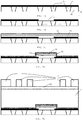
- FIG. 5 A process sequence for producing a transistor between two BEOL metallization layers is illustrated in Figure 5 .
- Figure 5a shows the upper level of a first metallization layer M n , comprising a number of metal lines 48, the intermetal dielectric 49 (this can be for example low K material, SiO 2 or air gap) and a passivation layer 50, e.g. a layer of SiCN.
- An opening 51 is etched in the passivation layer 50 by known litho/etch steps. The opening exposes at least a portion of two metal lines 52/53 in the M n layer.
- layers of IGZO and Al 2 O 3 54/55 are sequentially deposited by a suitable deposition technique ( Figure 5c ).
- a layer of between 10nm and 50nm of IGZO is deposited by PVD (Physical Vapour Deposition) and a layer of between 10nm and 50nm of Al 2 O 3 is deposited on and in contact with the IGZO by ALD (Atomic Layer Deposition). Suitable conditions for the PVD and ALD processes are known to the skilled reader and not described here in detail.
- a patterning of the IGZO/Al 2 O 3 stack is then performed, to obtain the stack 54/55 only on the required location ( Figure 5d ).
- An additional dielectric layer 56 for example a SiCN layer is deposited over the complete surface, covering the stack 56. This layer will act as etch stop layer during subsequent etching steps.
- the intermetal dielectric layer 57 of the next metallization layer M n+1 is deposited, followed by deposition of a Bottom Anti-Reflective Coating (BARC) layer 58, in turn followed by the deposition and patterning of a resist layer 59 ( Figure 5e ).
- BARC Bottom Anti-Reflective Coating
- the IMD layer 57 is etched a first time for forming trenches destined to be filled by metal lines in the upper level of M n+1 ( Figure 5f ), after which a second BARC 60 and resist 61 are deposited and the second resist is patterned, after which a second etching step is done, to form openings destined to be filled by interconnect vias in the lower level of M n+1 ( Figure 5g and 5h ).
- Etching of the vias stops on the etch stop layer 56. If the layer 55 can act as an etch stop layer, layer 56 may be omitted from the process. Vice versa, if layer 56 is a sufficiently good gate dielectric material, layer 55 could be omitted from the process (or layers 24/34 could be omitted from the devices of Figures 3 and 4 , and replaced by an etch stop layer).
- Metal deposition preferably deposition of a seed layer and electrodeposition of copper, into the patterned trenches and vias is performed for forming all metal lines and interconnects, including the transistor gate electrode 62 on top of the IGZO/Al 2 O 3 /SiCN stack ( Figure 5i ).
- the described method step sequence does not exclude the presence of other method steps in between the steps of the sequence.
- Method steps that are routinely applied during BEOL processing have not been included in the above description for the sake of conciseness.
- diffusion barrier layers will need to be deposited prior to deposition of metal lines and interconnect vias.
- a conductive layer is required that works as a diffusion barrier to the Cu. This can be e.g. a layer of Co, TaN, TiN.
- the thin film semiconductor material that is applicable in an FPGA according to the invention must be suitable for producing a low leakage select transistor T2, so that the memory cell can be used as a DRAM cell.
- the thin film semiconductor layer is furthermore a layer that can be deposited, for example by PVD, CVD, ALD, solution deposition, on an amorphous substrate, i.e. it does not require a crystalline template.
- the thin film semiconductor must also be compatible with the thermal budget of BEOL processing, i.e. the material must not degrade at the temperatures used in the BEOL part of the FPGA's production process (typically 350-380°C).
- IGZO is a preferred option for the thin film semiconductor, but other materials may be possible, such as amorphous silicon, monocrystalline or polycrystalline silicon, graphene, Carbon nano tubes or metal oxides other than IGZO, e.g. ZnO, HfInZnO, SnO, CuO.
- the gate electrodes 22/32 of T1 and T2 are metal-filled interconnect vias at the top of the transistors T1/T2 while the source and drain electrodes (20/21 for T1 and 30/31 for T2) are metal lines at the bottom of the transistors. This is the preferred embodiment, given that the signal for selecting the pass transistor arrives from outside the FPGA, i.e. from the upper metallization levels.
- both the T1 and T2 transistors have the gate electrode formed by a metal line at the bottom of the transistor, in a first metallization layer, and the source and drain electrodes formed by a pair of interconnect vias at the top of transistor, in a second metallization layer on top of the first (the first and second metallization layers being not necessarily the same for T1 and T2).
- the invention does not exclude that only one of the transistors T1 and T2 is located in the BEOL portion of the FPGA. In that case the other transistor would still be located in the FEOL portion, while the electrical connection between the two is established through a suitable design of via connections and metal lines in the metallization layers that are present between the BEOL transistor and the FEOL transistor.
- the description of a layer being present, deposited or produced 'on' another layer or substrate includes the options of
Landscapes
- Physics & Mathematics (AREA)
- Mathematical Physics (AREA)
- Engineering & Computer Science (AREA)
- Computer Hardware Design (AREA)
- Computing Systems (AREA)
- General Engineering & Computer Science (AREA)
- Design And Manufacture Of Integrated Circuits (AREA)
- Semiconductor Memories (AREA)
- Semiconductor Integrated Circuits (AREA)
Claims (8)
- Dispositif formant réseau prédiffusé programmable par l'utilisateur comprenant une portion d'extrémité avant de ligne (FEOL) et une portion d'extrémité arrière de ligne (BEOL), la portion BEOL comprenant une pluralité de couches de métallisation, la portion FEOL comprenant une pluralité de blocs logiques, le FPGA comprenant en outre des points d'interconnexion programmables (5) pour définir un routage de signaux entre lesdits blocs logiques et/ou entre d'autres portions du FPGA, dans lequel les points d'interconnexion comprennent un ou plusieurs transistors de passage (6), dans lequel chaque transistor de passage est équipé d'une cellule de mémoire vive dynamique (DRAM), ladite cellule DRAM comprenant un transistor de sélection (T2) connecté à une ligne de sélection et à une ligne de données, caractérisé en ce que ledit transistor de sélection et/ou ledit transistor de passage sont situés dans la portion BEOL du FPGA, dans lequel ledit transistor de sélection et/ou ledit transistor de passage situés dans la portion BEOL du FPGA comprennent des électrodes de source et de drain (20,21 ; 30,31), une électrode grille (22 ; 32), une région de canal (23 ; 33) et une région de diélectrique de grille (24 ; 34), et dans lequel :• les électrodes de source et de drain du transistor sont des lignes métalliques ou des couches intermédiaires d'interconnexion remplies de métal situées dans une première couche de métallisation de ladite portion BEOL,• l'électrode grille est respectivement une couche intermédiaire d'interconnexion remplie de métal ou une ligne métallique d'une seconde couche de métallisation de ladite portion BEOL, la seconde couche de métallisation étant directement adjacente à la première couche de métallisation,• la région de canal est une couche semi-conductrice (23 ; 33) sur lesdites électrodes de source et de drain (20,21 ; 30,31), et• le diélectrique de grille est une couche diélectrique (33 ; 34) sur la région de canal, avec l'électrode grille (32) se trouvant sur la couche de diélectrique de grille.
- FPGA selon la revendication 1, dans lequel ladite couche semi-conductrice (23 ; 33) est une couche d'oxyde indium gallium zinc (IGZO).
- FPGA selon l'une quelconque des revendications 1 ou 2, dans lequel le transistor de passage (T1) et le transistor de sélection (T2) sont tous les deux situés dans la portion BEOL du FPGA.
- FPGA selon la revendication 3, dans lequel le transistor de sélection (T2) et le transistor de passage (T1) sont situés dans trois couches de métallisation successives (Mn, Mn+1, Mn+2) de la portion BEOL, dans lequel la couche médiane (Mn+1) desdites trois couches comprend l'électrode grille de l'un desdits transistors et les électrodes de drain et de source de l'autre desdits transistors.
- FPGA selon la revendication 4, dans lequel le transistor de sélection (T2) et le transistor de passage (T1) sont tous les deux situés dans une paire (Mn, Mn+1) de couches de métallisation adjacentes de la portion BEOL.
- FPGA selon l'une quelconque des revendications précédentes, dans lequel la cellule de mémoire DRAM (7) comprend en outre un condensateur (C1) pour stocker la tension de grille du transistor de passage (T1), ledit condensateur étant également situé dans la portion BEOL du FPGA.
- FPGA selon la revendication 6, dans lequel le condensateur (C1) comprend une plaque inférieure (31), un diélectrique (34), et une plaque supérieure (35), la plaque inférieure étant formée par une ligne métallique ou une couche intermédiaire d'interconnexion dans une première couche de métallisation de la portion BEOL du FPGA, la plaque supérieure étant formée respectivement par une couche intermédiaire d'interconnexion ou une ligne métallique d'une seconde couche de métallisation du FPGA, la seconde couche de métallisation étant directement adjacente à la première couche de métallisation, et le diélectrique est placé entre les plaques inférieure et supérieure.
- FPGA selon la revendication 6, dans lequel la plaque inférieure ou supérieure du condensateur est formée par une couche intermédiaire d'interconnexion remplie de métal, ou une ligne métallique ou tout autre type de conducteur, qui forme également l'électrode de source ou de drain du transistor de sélection (T2).
Priority Applications (1)
| Application Number | Priority Date | Filing Date | Title |
|---|---|---|---|
| EP14191906.8A EP2884666B1 (fr) | 2013-12-10 | 2014-11-05 | Dispositif FPGA avec interconnexion programmable dans une partie d'extrémité arrière de ligne du dispositif |
Applications Claiming Priority (2)
| Application Number | Priority Date | Filing Date | Title |
|---|---|---|---|
| EP13196407 | 2013-12-10 | ||
| EP14191906.8A EP2884666B1 (fr) | 2013-12-10 | 2014-11-05 | Dispositif FPGA avec interconnexion programmable dans une partie d'extrémité arrière de ligne du dispositif |
Publications (2)
| Publication Number | Publication Date |
|---|---|
| EP2884666A1 EP2884666A1 (fr) | 2015-06-17 |
| EP2884666B1 true EP2884666B1 (fr) | 2019-01-02 |
Family
ID=49725069
Family Applications (1)
| Application Number | Title | Priority Date | Filing Date |
|---|---|---|---|
| EP14191906.8A Active EP2884666B1 (fr) | 2013-12-10 | 2014-11-05 | Dispositif FPGA avec interconnexion programmable dans une partie d'extrémité arrière de ligne du dispositif |
Country Status (3)
| Country | Link |
|---|---|
| US (1) | US9553586B2 (fr) |
| EP (1) | EP2884666B1 (fr) |
| KR (1) | KR101662906B1 (fr) |
Families Citing this family (9)
| Publication number | Priority date | Publication date | Assignee | Title |
|---|---|---|---|---|
| EP2884542A3 (fr) * | 2013-12-10 | 2015-09-02 | IMEC vzw | Dispositif de circuit intégré avec un commutateur à déclenchement de puissance à l'extrémité arrière de ligne |
| WO2017111798A1 (fr) * | 2015-12-23 | 2017-06-29 | Intel Corporation | Élément de mémoire à durée de rétention élevée avec dispositifs à double grille |
| US9520876B1 (en) | 2016-02-17 | 2016-12-13 | International Business Machines Corporation | Power gating and clock gating in wiring levels |
| WO2018004537A1 (fr) * | 2016-06-28 | 2018-01-04 | Intel Corporation | Intégration de transistors monocristallins dans la fin de ligne (beol) |
| US10644140B2 (en) * | 2016-06-30 | 2020-05-05 | Intel Corporation | Integrated circuit die having back-end-of-line transistors |
| US10403627B2 (en) | 2016-10-11 | 2019-09-03 | Imec Vzw | Memory device for a dynamic random access memory |
| US20190385657A1 (en) * | 2018-06-19 | 2019-12-19 | Intel Corporation | High density negative differential resistance based memory |
| EP3888783B1 (fr) * | 2020-04-01 | 2025-03-26 | Imec VZW | Adressage de nanoélectrodes dans un réseau de nanoélectrodes |
| US12324143B2 (en) | 2020-04-17 | 2025-06-03 | Micron Technology, Inc. | Methods of utilizing etch-stop material during fabrication of capacitors, integrated assemblies comprising capacitors |
Family Cites Families (21)
| Publication number | Priority date | Publication date | Assignee | Title |
|---|---|---|---|---|
| US5644496A (en) * | 1989-08-15 | 1997-07-01 | Advanced Micro Devices, Inc. | Programmable logic device with internal time-constant multiplexing of signals from external interconnect buses |
| US5847577A (en) * | 1995-02-24 | 1998-12-08 | Xilinx, Inc. | DRAM memory cell for programmable logic devices |
| US20020053694A1 (en) * | 1998-06-10 | 2002-05-09 | Sutcliffe Victor C. | Method of forming a memory cell with self-aligned contacts |
| US6144225A (en) * | 1999-03-03 | 2000-11-07 | Xilinx, Inc. | Programmable integrated circuit having metal plate capacitors that provide local switching energy |
| US7129744B2 (en) * | 2003-10-23 | 2006-10-31 | Viciciv Technology | Programmable interconnect structures |
| US7195931B2 (en) * | 2002-11-27 | 2007-03-27 | Advanced Micro Devices, Inc. | Split manufacturing method for advanced semiconductor circuits |
| US7030651B2 (en) * | 2003-12-04 | 2006-04-18 | Viciciv Technology | Programmable structured arrays |
| US8559209B2 (en) * | 2011-06-10 | 2013-10-15 | Unity Semiconductor Corporation | Array voltage regulating technique to enable data operations on large cross-point memory arrays with resistive memory elements |
| US8314024B2 (en) * | 2008-12-19 | 2012-11-20 | Unity Semiconductor Corporation | Device fabrication |
| US7764081B1 (en) * | 2005-08-05 | 2010-07-27 | Xilinx, Inc. | Programmable logic device (PLD) with memory refresh based on single event upset (SEU) occurrence to maintain soft error immunity |
| US8000519B1 (en) * | 2007-04-04 | 2011-08-16 | Xilinx, Inc. | Method of metal pattern inspection verification |
| US8435898B2 (en) * | 2007-04-05 | 2013-05-07 | Freescale Semiconductor, Inc. | First inter-layer dielectric stack for non-volatile memory |
| US7635843B1 (en) * | 2007-07-13 | 2009-12-22 | Xilinx, Inc. | In-line reliability test using E-beam scan |
| US20100157644A1 (en) * | 2008-12-19 | 2010-06-24 | Unity Semiconductor Corporation | Configurable memory interface to provide serial and parallel access to memories |
| US8456880B2 (en) * | 2009-01-30 | 2013-06-04 | Unity Semiconductor Corporation | Multiple layers of memory implemented as different memory technology |
| US8441038B1 (en) * | 2011-01-20 | 2013-05-14 | Xilinx, Inc. | Nano relay with floating bridge |
| US9117495B2 (en) * | 2011-06-10 | 2015-08-25 | Unity Semiconductor Corporation | Global bit line pre-charge circuit that compensates for process, operating voltage, and temperature variations |
| US8712718B1 (en) * | 2011-07-20 | 2014-04-29 | Xilinx, Inc. | Predicting performance of an integrated circuit |
| US8890562B1 (en) * | 2011-09-13 | 2014-11-18 | Xilinx, Inc. | At-speed testing of multi-die integrated circuits |
| US9177872B2 (en) * | 2011-09-16 | 2015-11-03 | Micron Technology, Inc. | Memory cells, semiconductor devices, systems including such cells, and methods of fabrication |
| US8952470B2 (en) * | 2012-09-10 | 2015-02-10 | James John Lupino | Low cost high density nonvolatile memory array device employing thin film transistors and back to back Schottky diodes |
-
2014
- 2014-11-05 EP EP14191906.8A patent/EP2884666B1/fr active Active
- 2014-12-09 US US14/565,316 patent/US9553586B2/en active Active
- 2014-12-10 KR KR1020140177323A patent/KR101662906B1/ko active Active
Non-Patent Citations (1)
| Title |
|---|
| None * |
Also Published As
| Publication number | Publication date |
|---|---|
| KR101662906B1 (ko) | 2016-10-05 |
| US9553586B2 (en) | 2017-01-24 |
| EP2884666A1 (fr) | 2015-06-17 |
| US20150162913A1 (en) | 2015-06-11 |
| KR20150067742A (ko) | 2015-06-18 |
Similar Documents
| Publication | Publication Date | Title |
|---|---|---|
| EP2884666A1 (fr) | Dispositif FPGA avec interconnexion programmable dans une partie d'extrémité arrière de ligne du dispositif | |
| EP2884542A2 (fr) | Dispositif de circuit intégré avec un commutateur à déclenchement de puissance à l'extrémité arrière de ligne | |
| CN109314116B (zh) | 用于形成三维存储器件的方法 | |
| US10103330B2 (en) | Resistance variable memory structure | |
| US20240387615A1 (en) | Semiconductor devices and methods for fabrication thereof | |
| US20150155235A1 (en) | Anti-fuse of semiconductor device, semiconductor module and system each including the semiconductor device, and method for forming the anti-fuse | |
| US10553789B1 (en) | Fully aligned semiconductor device with a skip-level via | |
| US20240405071A1 (en) | Stacked two-transistor dynamic random access memory cell | |
| US9406883B1 (en) | Structure and formation method of memory device | |
| US20240373650A1 (en) | Semiconductor device, integrated circuit and method of manufacturing the same | |
| CN222786243U (zh) | 反相器电路及半导体电路 | |
| CN222721870U (zh) | 反相器电路和半导体电路 | |
| US12568812B2 (en) | Back-end-of-line CMOS inverter having twin channels and one gate electrode and methods of forming the same | |
| US20090140310A1 (en) | Semiconductor device and method for manufacturing the same | |
| US11127784B2 (en) | Integrated circuits with embedded memory structures and methods for fabricating the same | |
| US20250024657A1 (en) | Semiconductor devices and methods of manufacturing thereof | |
| US20240105608A1 (en) | Local frontside power rail with global backside power delivery | |
| US12419057B2 (en) | Semiconductor device, integrated circuit and method of manufacturing the same | |
| CN103633241B (zh) | 忆阻存储器及其制造方法 | |
| CN222424606U (zh) | 半导体装置结构及半导体装置 | |
| Tada et al. | Three-terminal nonvolatile resistive-change device integrated in Cu-BEOL | |
| WO2026044677A1 (fr) | Structures semi-conductrices et leur procédé de fabrication | |
| CN100550428C (zh) | 一种非易失性存储器件及其设计方法 |
Legal Events
| Date | Code | Title | Description |
|---|---|---|---|
| PUAI | Public reference made under article 153(3) epc to a published international application that has entered the european phase |
Free format text: ORIGINAL CODE: 0009012 |
|
| 17P | Request for examination filed |
Effective date: 20141105 |
|
| AK | Designated contracting states |
Kind code of ref document: A1 Designated state(s): AL AT BE BG CH CY CZ DE DK EE ES FI FR GB GR HR HU IE IS IT LI LT LU LV MC MK MT NL NO PL PT RO RS SE SI SK SM TR |
|
| AX | Request for extension of the european patent |
Extension state: BA ME |
|
| R17P | Request for examination filed (corrected) |
Effective date: 20151207 |
|
| RBV | Designated contracting states (corrected) |
Designated state(s): AL AT BE BG CH CY CZ DE DK EE ES FI FR GB GR HR HU IE IS IT LI LT LU LV MC MK MT NL NO PL PT RO RS SE SI SK SM TR |
|
| STAA | Information on the status of an ep patent application or granted ep patent |
Free format text: STATUS: EXAMINATION IS IN PROGRESS |
|
| 17Q | First examination report despatched |
Effective date: 20180322 |
|
| GRAP | Despatch of communication of intention to grant a patent |
Free format text: ORIGINAL CODE: EPIDOSNIGR1 |
|
| STAA | Information on the status of an ep patent application or granted ep patent |
Free format text: STATUS: GRANT OF PATENT IS INTENDED |
|
| INTG | Intention to grant announced |
Effective date: 20180720 |
|
| GRAS | Grant fee paid |
Free format text: ORIGINAL CODE: EPIDOSNIGR3 |
|
| GRAA | (expected) grant |
Free format text: ORIGINAL CODE: 0009210 |
|
| STAA | Information on the status of an ep patent application or granted ep patent |
Free format text: STATUS: THE PATENT HAS BEEN GRANTED |
|
| AK | Designated contracting states |
Kind code of ref document: B1 Designated state(s): AL AT BE BG CH CY CZ DE DK EE ES FI FR GB GR HR HU IE IS IT LI LT LU LV MC MK MT NL NO PL PT RO RS SE SI SK SM TR |
|
| REG | Reference to a national code |
Ref country code: GB Ref legal event code: FG4D |
|
| REG | Reference to a national code |
Ref country code: CH Ref legal event code: EP Ref country code: AT Ref legal event code: REF Ref document number: 1085716 Country of ref document: AT Kind code of ref document: T Effective date: 20190115 |
|
| REG | Reference to a national code |
Ref country code: IE Ref legal event code: FG4D |
|
| REG | Reference to a national code |
Ref country code: DE Ref legal event code: R096 Ref document number: 602014039022 Country of ref document: DE |
|
| REG | Reference to a national code |
Ref country code: NL Ref legal event code: MP Effective date: 20190102 |
|
| REG | Reference to a national code |
Ref country code: LT Ref legal event code: MG4D |
|
| REG | Reference to a national code |
Ref country code: AT Ref legal event code: MK05 Ref document number: 1085716 Country of ref document: AT Kind code of ref document: T Effective date: 20190102 |
|
| PG25 | Lapsed in a contracting state [announced via postgrant information from national office to epo] |
Ref country code: NL Free format text: LAPSE BECAUSE OF FAILURE TO SUBMIT A TRANSLATION OF THE DESCRIPTION OR TO PAY THE FEE WITHIN THE PRESCRIBED TIME-LIMIT Effective date: 20190102 |
|
| PG25 | Lapsed in a contracting state [announced via postgrant information from national office to epo] |
Ref country code: PT Free format text: LAPSE BECAUSE OF FAILURE TO SUBMIT A TRANSLATION OF THE DESCRIPTION OR TO PAY THE FEE WITHIN THE PRESCRIBED TIME-LIMIT Effective date: 20190502 Ref country code: ES Free format text: LAPSE BECAUSE OF FAILURE TO SUBMIT A TRANSLATION OF THE DESCRIPTION OR TO PAY THE FEE WITHIN THE PRESCRIBED TIME-LIMIT Effective date: 20190102 Ref country code: NO Free format text: LAPSE BECAUSE OF FAILURE TO SUBMIT A TRANSLATION OF THE DESCRIPTION OR TO PAY THE FEE WITHIN THE PRESCRIBED TIME-LIMIT Effective date: 20190402 Ref country code: FI Free format text: LAPSE BECAUSE OF FAILURE TO SUBMIT A TRANSLATION OF THE DESCRIPTION OR TO PAY THE FEE WITHIN THE PRESCRIBED TIME-LIMIT Effective date: 20190102 Ref country code: LT Free format text: LAPSE BECAUSE OF FAILURE TO SUBMIT A TRANSLATION OF THE DESCRIPTION OR TO PAY THE FEE WITHIN THE PRESCRIBED TIME-LIMIT Effective date: 20190102 Ref country code: SE Free format text: LAPSE BECAUSE OF FAILURE TO SUBMIT A TRANSLATION OF THE DESCRIPTION OR TO PAY THE FEE WITHIN THE PRESCRIBED TIME-LIMIT Effective date: 20190102 Ref country code: PL Free format text: LAPSE BECAUSE OF FAILURE TO SUBMIT A TRANSLATION OF THE DESCRIPTION OR TO PAY THE FEE WITHIN THE PRESCRIBED TIME-LIMIT Effective date: 20190102 |
|
| PG25 | Lapsed in a contracting state [announced via postgrant information from national office to epo] |
Ref country code: GR Free format text: LAPSE BECAUSE OF FAILURE TO SUBMIT A TRANSLATION OF THE DESCRIPTION OR TO PAY THE FEE WITHIN THE PRESCRIBED TIME-LIMIT Effective date: 20190403 Ref country code: BG Free format text: LAPSE BECAUSE OF FAILURE TO SUBMIT A TRANSLATION OF THE DESCRIPTION OR TO PAY THE FEE WITHIN THE PRESCRIBED TIME-LIMIT Effective date: 20190402 Ref country code: RS Free format text: LAPSE BECAUSE OF FAILURE TO SUBMIT A TRANSLATION OF THE DESCRIPTION OR TO PAY THE FEE WITHIN THE PRESCRIBED TIME-LIMIT Effective date: 20190102 Ref country code: HR Free format text: LAPSE BECAUSE OF FAILURE TO SUBMIT A TRANSLATION OF THE DESCRIPTION OR TO PAY THE FEE WITHIN THE PRESCRIBED TIME-LIMIT Effective date: 20190102 Ref country code: IS Free format text: LAPSE BECAUSE OF FAILURE TO SUBMIT A TRANSLATION OF THE DESCRIPTION OR TO PAY THE FEE WITHIN THE PRESCRIBED TIME-LIMIT Effective date: 20190502 Ref country code: LV Free format text: LAPSE BECAUSE OF FAILURE TO SUBMIT A TRANSLATION OF THE DESCRIPTION OR TO PAY THE FEE WITHIN THE PRESCRIBED TIME-LIMIT Effective date: 20190102 |
|
| REG | Reference to a national code |
Ref country code: DE Ref legal event code: R097 Ref document number: 602014039022 Country of ref document: DE |
|
| PG25 | Lapsed in a contracting state [announced via postgrant information from national office to epo] |
Ref country code: SK Free format text: LAPSE BECAUSE OF FAILURE TO SUBMIT A TRANSLATION OF THE DESCRIPTION OR TO PAY THE FEE WITHIN THE PRESCRIBED TIME-LIMIT Effective date: 20190102 Ref country code: IT Free format text: LAPSE BECAUSE OF FAILURE TO SUBMIT A TRANSLATION OF THE DESCRIPTION OR TO PAY THE FEE WITHIN THE PRESCRIBED TIME-LIMIT Effective date: 20190102 Ref country code: RO Free format text: LAPSE BECAUSE OF FAILURE TO SUBMIT A TRANSLATION OF THE DESCRIPTION OR TO PAY THE FEE WITHIN THE PRESCRIBED TIME-LIMIT Effective date: 20190102 Ref country code: CZ Free format text: LAPSE BECAUSE OF FAILURE TO SUBMIT A TRANSLATION OF THE DESCRIPTION OR TO PAY THE FEE WITHIN THE PRESCRIBED TIME-LIMIT Effective date: 20190102 Ref country code: AT Free format text: LAPSE BECAUSE OF FAILURE TO SUBMIT A TRANSLATION OF THE DESCRIPTION OR TO PAY THE FEE WITHIN THE PRESCRIBED TIME-LIMIT Effective date: 20190102 Ref country code: EE Free format text: LAPSE BECAUSE OF FAILURE TO SUBMIT A TRANSLATION OF THE DESCRIPTION OR TO PAY THE FEE WITHIN THE PRESCRIBED TIME-LIMIT Effective date: 20190102 Ref country code: AL Free format text: LAPSE BECAUSE OF FAILURE TO SUBMIT A TRANSLATION OF THE DESCRIPTION OR TO PAY THE FEE WITHIN THE PRESCRIBED TIME-LIMIT Effective date: 20190102 Ref country code: DK Free format text: LAPSE BECAUSE OF FAILURE TO SUBMIT A TRANSLATION OF THE DESCRIPTION OR TO PAY THE FEE WITHIN THE PRESCRIBED TIME-LIMIT Effective date: 20190102 |
|
| PLBE | No opposition filed within time limit |
Free format text: ORIGINAL CODE: 0009261 |
|
| STAA | Information on the status of an ep patent application or granted ep patent |
Free format text: STATUS: NO OPPOSITION FILED WITHIN TIME LIMIT |
|
| PG25 | Lapsed in a contracting state [announced via postgrant information from national office to epo] |
Ref country code: SM Free format text: LAPSE BECAUSE OF FAILURE TO SUBMIT A TRANSLATION OF THE DESCRIPTION OR TO PAY THE FEE WITHIN THE PRESCRIBED TIME-LIMIT Effective date: 20190102 |
|
| 26N | No opposition filed |
Effective date: 20191003 |
|
| PG25 | Lapsed in a contracting state [announced via postgrant information from national office to epo] |
Ref country code: SI Free format text: LAPSE BECAUSE OF FAILURE TO SUBMIT A TRANSLATION OF THE DESCRIPTION OR TO PAY THE FEE WITHIN THE PRESCRIBED TIME-LIMIT Effective date: 20190102 |
|
| PG25 | Lapsed in a contracting state [announced via postgrant information from national office to epo] |
Ref country code: TR Free format text: LAPSE BECAUSE OF FAILURE TO SUBMIT A TRANSLATION OF THE DESCRIPTION OR TO PAY THE FEE WITHIN THE PRESCRIBED TIME-LIMIT Effective date: 20190102 |
|
| REG | Reference to a national code |
Ref country code: CH Ref legal event code: PL |
|
| PG25 | Lapsed in a contracting state [announced via postgrant information from national office to epo] |
Ref country code: LI Free format text: LAPSE BECAUSE OF NON-PAYMENT OF DUE FEES Effective date: 20191130 Ref country code: LU Free format text: LAPSE BECAUSE OF NON-PAYMENT OF DUE FEES Effective date: 20191105 Ref country code: CH Free format text: LAPSE BECAUSE OF NON-PAYMENT OF DUE FEES Effective date: 20191130 Ref country code: MC Free format text: LAPSE BECAUSE OF FAILURE TO SUBMIT A TRANSLATION OF THE DESCRIPTION OR TO PAY THE FEE WITHIN THE PRESCRIBED TIME-LIMIT Effective date: 20190102 |
|
| REG | Reference to a national code |
Ref country code: BE Ref legal event code: MM Effective date: 20191130 |
|
| GBPC | Gb: european patent ceased through non-payment of renewal fee |
Effective date: 20191105 |
|
| PG25 | Lapsed in a contracting state [announced via postgrant information from national office to epo] |
Ref country code: IE Free format text: LAPSE BECAUSE OF NON-PAYMENT OF DUE FEES Effective date: 20191105 Ref country code: GB Free format text: LAPSE BECAUSE OF NON-PAYMENT OF DUE FEES Effective date: 20191105 |
|
| PG25 | Lapsed in a contracting state [announced via postgrant information from national office to epo] |
Ref country code: BE Free format text: LAPSE BECAUSE OF NON-PAYMENT OF DUE FEES Effective date: 20191130 |
|
| PG25 | Lapsed in a contracting state [announced via postgrant information from national office to epo] |
Ref country code: CY Free format text: LAPSE BECAUSE OF FAILURE TO SUBMIT A TRANSLATION OF THE DESCRIPTION OR TO PAY THE FEE WITHIN THE PRESCRIBED TIME-LIMIT Effective date: 20190102 |
|
| PG25 | Lapsed in a contracting state [announced via postgrant information from national office to epo] |
Ref country code: HU Free format text: LAPSE BECAUSE OF FAILURE TO SUBMIT A TRANSLATION OF THE DESCRIPTION OR TO PAY THE FEE WITHIN THE PRESCRIBED TIME-LIMIT; INVALID AB INITIO Effective date: 20141105 Ref country code: MT Free format text: LAPSE BECAUSE OF FAILURE TO SUBMIT A TRANSLATION OF THE DESCRIPTION OR TO PAY THE FEE WITHIN THE PRESCRIBED TIME-LIMIT Effective date: 20190102 |
|
| PG25 | Lapsed in a contracting state [announced via postgrant information from national office to epo] |
Ref country code: MK Free format text: LAPSE BECAUSE OF FAILURE TO SUBMIT A TRANSLATION OF THE DESCRIPTION OR TO PAY THE FEE WITHIN THE PRESCRIBED TIME-LIMIT Effective date: 20190102 |
|
| P01 | Opt-out of the competence of the unified patent court (upc) registered |
Effective date: 20230513 |
|
| PGFP | Annual fee paid to national office [announced via postgrant information from national office to epo] |
Ref country code: DE Payment date: 20251022 Year of fee payment: 12 |
|
| PGFP | Annual fee paid to national office [announced via postgrant information from national office to epo] |
Ref country code: FR Payment date: 20251022 Year of fee payment: 12 |