EP2885805B1 - Sicherungsausfallanzeige - Google Patents
Sicherungsausfallanzeige Download PDFInfo
- Publication number
- EP2885805B1 EP2885805B1 EP13750866.9A EP13750866A EP2885805B1 EP 2885805 B1 EP2885805 B1 EP 2885805B1 EP 13750866 A EP13750866 A EP 13750866A EP 2885805 B1 EP2885805 B1 EP 2885805B1
- Authority
- EP
- European Patent Office
- Prior art keywords
- fuse
- current path
- effect transistor
- voltage
- parallel
- Prior art date
- Legal status (The legal status is an assumption and is not a legal conclusion. Google has not performed a legal analysis and makes no representation as to the accuracy of the status listed.)
- Active
Links
Images
Classifications
-
- H—ELECTRICITY
- H01—ELECTRIC ELEMENTS
- H01H—ELECTRIC SWITCHES; RELAYS; SELECTORS; EMERGENCY PROTECTIVE DEVICES
- H01H85/00—Protective devices in which the current flows through a part of fusible material and this current is interrupted by displacement of the fusible material when this current becomes excessive
- H01H85/02—Details
- H01H85/30—Means for indicating condition of fuse structurally associated with the fuse
- H01H85/32—Indicating lamp structurally associated with the protective device
-
- H—ELECTRICITY
- H02—GENERATION; CONVERSION OR DISTRIBUTION OF ELECTRIC POWER
- H02H—EMERGENCY PROTECTIVE CIRCUIT ARRANGEMENTS
- H02H3/00—Emergency protective circuit arrangements for automatic disconnection directly responsive to an undesired change from normal electric working condition with or without subsequent reconnection ; integrated protection
- H02H3/02—Details
- H02H3/04—Details with warning or supervision in addition to disconnection, e.g. for indicating that protective apparatus has functioned
- H02H3/046—Signalling the blowing of a fuse
-
- H—ELECTRICITY
- H01—ELECTRIC ELEMENTS
- H01H—ELECTRIC SWITCHES; RELAYS; SELECTORS; EMERGENCY PROTECTIVE DEVICES
- H01H85/00—Protective devices in which the current flows through a part of fusible material and this current is interrupted by displacement of the fusible material when this current becomes excessive
- H01H85/02—Details
- H01H85/0241—Structural association of a fuse and another component or apparatus
- H01H2085/0283—Structural association with a semiconductor device
Definitions
- the invention relates to a circuit for fuse failure indication for monitoring the triggering status of a fuse, wherein a light-emitting diode is provided for displaying the triggering status of the fuse.
- the invention is intended for use in monitoring fuses in both DC and AC operation. It is suitable for wide-range use to monitor low-voltage fuses from a few volts to a few hundred volts. With appropriate dimensioning of the semiconductor components to be used but also the use in high voltage range is basically possible.
- Object of the present invention is to provide a simple and inexpensive, usable in a wide voltage range and realizable in a small space circuit for fuse monitoring, which is suitable for both DC and AC operation.
- a circuit arrangement for fuse failure indication for monitoring the triggering status of a fuse which has a light-emitting diode to display the triggering status of the fuse, which is arranged in a current path parallel to the fuse, with not triggered fuse this parallel current path has such a high resistance in relation to the resistance across the fuse that the current across this current path is insufficient to operate the LED, and when the fuse is blown, this parallel current path has such a low resistance relative to the resistor across the fuse the current is sufficient over this current path for operating the light-emitting diode, further comprising a current limiting device for limiting the current across the light emitting diode and a voltage limiting device for limiting the voltage across the tripped fuse, wherein b
- a field-effect transistor and a resistor are provided in series, and when the fuse is blown to establish the current-limiting device in the parallel current path, the same resistor is provided form
- the circuit protected by the fuse will remain closed across the parallel current path of the fuse failure indicator, a current limiting device limiting the current via the fuse failure indication and thus simultaneously operating a light emitting diode.
- a first advantage is that the circuit requires very few components. It is thus inexpensive and to realize a small footprint. In many security applications, it will thus be able to be integrated into existing housings.
- the circuit is usable independently of the operating voltage. Only limited by the dielectric strength of the semiconductor, the field effect transistor regulates the current through the parallel current path even at high voltages between the terminals of the fuse failure indicator down to a preset size, so that the LED is not destroyed.
- the arrangement is suitable for both the DC operation and the AC operation, wherein in the latter is preferably provided due to the LED used a half-wave rectification.
- the circuit has a varistor which is arranged in a further parallel current path parallel to the fuse.
- the circuit for voltage limiting device further comprises a capacitor which is arranged in a further parallel current path parallel to the fuse.
- the circuit therefore has both a varistor and a capacitor.
- the circuit is further designed such that the series circuit comprises two additional diodes, which frame the arrangement of field effect transistor, resistor and light-emitting diode, for example.
- the circuit is further designed such that the light-emitting diode is part of an optocoupler or the series circuit additionally comprises an optocoupler, via which a feedback or a coupling can be made to a transmitter.
- an optocoupler has the advantage of galvanic isolation from the circuit protected by the fuse, so that, for example, possible voltage peaks can not act on a subsequent evaluation electronics.
- the field effect transistor is designed as a MOSFET (Metal Oxide Semiconductor Field Effect Transistor), which has a negative temperature coefficient, so that its resistance increases, if it is overloaded by too high a current.
- MOSFET Metal Oxide Semiconductor Field Effect Transistor
- a self-conducting n-channel MOSFET is suitable, which blocks the source-drain channel with increasing (negative) gate voltage.
- a voltage suitable as a control voltage is applied across the resistor.
- a protective diode is further arranged between the source and drain of the field effect transistor, wherein the field effect transistor may be configured to include this protection diode.
- the protective diode is designed as a Zener diode, which conducts from a predetermined threshold voltage against the reverse direction.
- this can be integrated into the component of the field effect transistor.
- the circuit according to the invention comprises a varistor, a capacitor, a resistor, a field effect transistor, a light emitting diode and two diodes, and optionally an optocoupler.
- a good ratio of circuit complexity to reliable functionality and space requirements is achieved.
- a safety device has a fuse failure indicator with the features described above.
- This may be, for example, a series fuse terminal, a circuit breaker, a device for a G-fuse or a holder for a Feinellotechnisch.
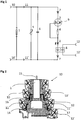
- FIG. 1 shows a circuit for fuse failure display according to a preferred embodiment of the invention.
- the circuit to be fused via the fuse 1 can be connected to the fuse 1 via the connection contacts 10, 10 '.
- the circuit of the fuse failure indicator is connected in parallel via the connection contacts 11, 11 'of the fuse failure indicator to the fuse 1.
- the circuit of the fuse failure indicator has three parallel current paths between its terminal contacts 11 and 11 '.
- a first runs via the varistor 5, a second via the capacitor 6 and a third via a series connection of two diodes, 7, an n-channel field effect transistor 3 with integrated protective diode 9, a resistor 4, a light emitting diode 2 and an optocoupler.
- 8 Unless specified in greater detail, the term "parallel current path" below refers to the last-mentioned series connection.
- the sensor connections or connection contacts for the feedback 12, 12 'of the optocoupler 8 are galvanically isolated from the circuit to be protected and switched by the optocoupler 8. If the fuse is not triggered, the circuit to be protected is closed both via fuse 1 and via the parallel current path of the fuse failure indicator. In this case represent fuse 1 and fuse failure indication from the point of view of the circuit to be hedged a current divider. The current is distributed inversely proportional to the resistance to the branches of the fuse and the power failure indicator.
- the parallel current path associated with the resistor 4 inevitably has a comparatively high resistance.
- the current flows at not triggered fuse 1 almost exclusively on the almost resistance-free fuse 1.
- the terminals of the fuse 10, 10 'and the fuse failure indicator 11, 11' are at the same potential, it flows not sufficiently high current through the parallel current path to the to operate the LED 2 of the fuse failure indicator.
- the terminals of the varistor 5 are at the same potential, so that even this is in the off state due to lack of applied voltage.
- the capacitor 6 is an insulator, provided that both poles are at the same potential.
- the fuse 1 is in the tripped state, it represents an insulator with almost infinite resistance. The circuit is still closed in this case, but now on the parallel current path of the fuse failure indicator.
- the field effect transistor 3 is designed as a self-conducting n-channel field effect transistor, so that it already without Concerns a gate voltage conducts. At the moment of the fuse failure, it is therefore in the conducting state without significant resistance.
- the resistance of the parallel current path is first determined by the resistor 4. With, due to the failure of the fuse 1, increasingly increasing current through the resistor 4, falls across the resistor 4 from a voltage , which is supplied to the field effect transistor 3 as a negative control voltage between the gate and source. The field effect transistor 3 thus goes into the blocking state until the current flowing through has settled to a value that can be predetermined by the resistance value of the resistor 4.
- the current through the parallel current path of the fuse failure indicator is thus in a wide voltage range independent of the operating voltage of the hedged circuit.
- the capacitor 6 is adapted to keep the voltage between the terminals 11 and 11 'stable, so that the parallel current path is protected from voltage spikes.
- FIG. 2 shows an embodiment of a row fuse terminal 13 with a fuse failure indicator according to the invention.
- the circuit of the fuse failure indicator is disposed on a circuit board 14, which together with the Fuse 1 is integrated in the row fuse terminal 13.
- the row fuse terminal 13 has a plurality of terminal contacts 10, 10 ', 12, 12', which can be designed as terminals, for example as a push-in.
- About the connection contacts 10, 10 ' is the connection of the hedged circuit.
- Via the connection contacts 12, 12 ' is optionally the connection of the feedback. It can be waived by abandoning the galvanic isolation on one of the connection contacts 12 or 12 '.
- connection contacts 10, 10 ' are connected via the internal wiring of the fuse failure indicator with the fuse 1 and the terminal contacts of the fuse failure indicator 11, 11'.
- the connection contacts 12, 12 'of an optional feedback circuit are connected via the wiring of the feedback 17 with the also optional optocoupler 8 of the circuit.
- the fuse 1 can be actuated mechanically via the rotary device 15. LIST OF REFERENCE NUMBERS fuse 1 led 2 Field Effect Transistor 3 resistance 4 varistor 5 capacitor 6 diode 7 optocoupler 8th protection diode 9 Connection contact fuse 10, 10 ' Connection contact Fuse failure indicator 11, 11 ' Connection contact feedback 12, 12 ' Row fuse with fuse failure indicator 13 circuit board 14 rotator 15 Wiring Fuse failure indicator 16 Wiring feedback 17
Landscapes
- Fuses (AREA)
- Emergency Protection Circuit Devices (AREA)
Description
- Die Erfindung betrifft eine Schaltung zur Sicherungsausfallanzeige für eine Überwachung des Auslöse-Status einer Sicherung, wobei zur Anzeige des Auslöse-Status der Sicherung eine Leuchtdiode vorgesehen ist.
- Die Erfindung ist für einen Einsatz zur Überwachung von Sicherungen sowohl im Gleichstrombetrieb als auch im Wechselstrombetrieb vorgesehen. Sie ist geeignet im Weitbereichseinsatz Sicherungen im Niederspannungsbereich von wenigen Volt bis einigen hundert Volt zu überwachen. Bei entsprechender Dimensionierung der zu verwendenden Halbleiterkomponenten ist aber auch der Einsatz im Hochspannungsbereich grundsätzlich möglich.
- Die Anforderung, den Status von Sicherungen optisch oder elektronisch überwachen zu können, ist vielfach begründet. Kleingerätesicherungen sind oftmals schlecht zugänglich, zudem ist der Zustand eines Schmelzdrahtes einer Feinsicherung oftmals schwer zu erkennen. In einem anderen Leistungsbereich sind beispielsweise die Stellungen der Leitungsschutzschalter einer Hausverteilung bei Dunkelheit nicht zu erkennen. Und in einem weiteren Einsatzbereich erfordert eine elektrische Steuerungs- oder Überwachungsanlage gegebenenfalls den Status einer Sicherung als Sensorinformation zur Fehleranzeige oder zum Einleiten von Maßnahmen.
- Entsprechend der individuellen Problemstellung sind aus dem Stand der Technik auf die jeweilige Situation zugeschnittene, oftmals aufwändige Lösungen bekannt.
- Das Dokument
DE 2831139 offenbart die Merkmale des Oberbegriffs des Anspruchs 1. - Aufgabe der vorliegenden Erfindung ist es, eine einfache und preisgünstige, in einem weiten Spannungsbereich einsetzbare und auf kleinem Raum realisierbare Schaltung zur Sicherungsüberwachung anzugeben, die sowohl für den Gleichstrom- als auch den Wechselstrombetrieb geeignet ist.
- Die Lösung der Aufgabe erfolgt erfindungsgemäß durch die Merkmale des unabhängigen Anspruchs. Vorteilhafte Ausgestaltungen der Erfindung sind in den Unteransprüchen angegeben.
- Erfindungsgemäß ist damit eine Schaltungsanordnung zur Sicherungsausfallanzeige für eine Überwachung des Auslöse-Status einer Sicherung vorgesehen, welche zur Anzeige des Auslöse-Status der Sicherung eine Leuchtdiode aufweist, die in einem Strompfad parallel zu der Sicherung angeordnet ist, wobei bei nicht ausgelöster Sicherung dieser parallele Strompfad im Verhältnis zu dem Widerstand über die Sicherung einen derart hohen Widerstand aufweist, dass der Strom über diesen Strompfad zum Betreiben der Leuchtdiode nicht ausreicht, und wobei bei ausgelöster Sicherung dieser parallele Strompfad im Verhältnis zu dem Widerstand über die Sicherung einen derart niedrigen Widerstand aufweist, dass der Strom über diesen Strompfad zum Betreiben der Leuchtdiode ausreicht, wobei ferner eine Strombegrenzungseinrichtung zur Begrenzung des Stroms über die Leuchtdiode und eine Spannungsbegrenzungseinrichtung zur Begrenzung der Spannung über die ausgelöste Sicherung vorgesehen ist, wobei bei nicht ausgelöster Sicherung zur Erzielung des hohen Widerstands des parallelen Strompfades ein Feldeffekttransistor und ein Widerstand in Reihe vorgesehen sind und bei ausgelöster Sicherung zur Einrichtung der Strombegrenzungseinrichtung in dem parallelen Strompfad derselbe Widerstand vorgesehen ist, um eine Steuerspannung für den Feldeffekttransistor in dem parallelen Strompfad mit der Leuchtdiode auszubilden, von der der Sperrzustand des Feldeffekttransistor abhängig ist.
- Mit anderen Worten ist vorgesehen, dass nach einem Ausfall der zu überwachenden Sicherung der über die Sicherung abgesicherte Stromkreis über den parallelen Strompfad der Sicherungsausfallanzeige weiterhin geschlossen bleibt, wobei eine Strombegrenzungseinrichtung den Strom über die Sicherungsausfallanzeige begrenzt und damit gleichzeitig eine Leuchtdiode betreibt.
- Die Anordnung weist dabei mehrere Vorteile auf.
Ein erster Vorteil besteht darin, dass die Schaltung nur sehr wenige Bauelemente benötigt. Sie ist damit kostengünstig und mit geringem Raumbedarf zu realisieren. In vielen Sicherungsanwendungen wird sie damit in bestehende Gehäuse integrierbar sein. - Ein weiterer Vorteil besteht darin, dass die Schaltung unabhängig von der Betriebsspannung verwendbar ist. Lediglich begrenzt durch die Spannungsfestigkeit der Halbleiter regelt der Feldeffekttransistor den Strom durch den parallelen Strompfad auch bei hohen Spannungen zwischen den Anschlusskontakten der Sicherungsausfallanzeige auf eine voreingestellte Größe herunter, so dass die Leuchtdiode nicht zerstört wird.
- Die Anordnung ist sowohl für den Gleichstrombetrieb als auch den Wechselstrombetrieb geeignet, wobei bei letzterem aufgrund der verwendeten Leuchtdiode vorzugsweise eine Halbwellengleichrichtung vorgesehen ist.
- Vorteilhaft weist die Schaltung einen Varistor auf, der in einem weiteren parallelen Strompfad parallel zur Sicherung angeordnet ist.
- Der Vorteil eines solchen spannungsabhängigen Widerstands ist, dass sein Widerstand bei Anliegen einer vorgegebenen Schwellspannung abrupt sinkt und er damit leitend wird. Dabei muss die vorgegebene Schwellspannung oberhalb der Betriebsspannung liegen, so dass der Varistor nur für Spannungsspitzen oberhalb der Betriebsspannung leitend wird und dadurch den parallelen Strompfad mit dem Feldeffekttransistor schützt.
- Vorteilhaft weist die Schaltung zur Spannungsbegrenzungseinrichtung ferner einen Kondensator auf, der in einem weiteren parallelen Strompfad parallel zur Sicherung angeordnet ist.
- Bei nicht ausgelöster Sicherung sind die Pole des Kondensators über die Sicherung kurzgeschlossen, so dass der Kondensator vollständig entladen ist. Aufgrund von Induktivitäten in dem von der Sicherung abgesicherten Stromkreises könnte es bei dem Auslösen der Sicherung zu Spannungsspitzen kommen, sofern diese nicht von dem Kondensator kompensiert würden. Vorteilhaft weist die Schaltung daher sowohl einen Varistor als auch einen Kondensator auf.
- Vorteilhaft ist die Schaltung ferner derart ausgebildet, dass die Reihenschaltung zwei zusätzliche Dioden aufweist, die die Anordnung aus Feldeffekttransistor, Widerstand und Leuchtdiode beispielsweise umrahmen.
- Auch diese bieten dem von ihnen umrahmten Feldeffekttransistor zusätzlichen Schutz gegen Überspannung. Desweiteren sind sie bei Wechselstrombetrieb geeignet, die Halbwellengleichrichtung zu übernehmen und so die Leuchtdiode zu entlasten.
- Vorteilhaft ist die Schaltung weiterhin derart ausgebildet, dass die Leuchtiode Teil eines Optokoppler ist oder die Reihenschaltung zusätzlich einen Optokoppler aufweist, über den eine Rückmeldung oder eine Kopplung an eine Auswerteelektronik erfolgen kann.
- Dabei weist ein Optokoppler den Vorteil der galvanischen, Trennung von dem von der Sicherung abgesicherten Stromkreis auf, so dass beispielsweise mögliche Spannungsspitzen nicht auf eine nachgeschaltete Auswerteelektronik einwirken können.
- Vorteilhaft ist der Feldeffekttransistor als MOSFET (Metal Oxide Semiconductor Field Effect Transistor) ausgebildet, der einen negativen Temperaturkoeffizienten aufweist, so dass sein Widerstand steigt, sofern er von einem zu hohem Strom überlastet wird.
- Zur Ausbildung der Stromregelung ist beispielsweise ein selbstleitender n-Kanal-MOSFET geeignet, der den Source-Drain-Kanal mit zunehmender (negativer) Gate-Spannung sperrt. Bei einem Strom durch den Widerstand der Schaltung fällt über den Widerstand eine solche als Steuerspannung geeignete Spannung an.
- Vorteilhaft ist ferner zwischen Source und Drain des Feldeffekttransistors eine Schutzdiode angeordnet, wobei der Feldeffekttransistor so ausgebildet sein kann, dass er diese Schutzdiode beinhaltet.
- Aufgrund der hohen Anfälligkeit gegenüber Überspannungsspitzen, auch durch Elektrostatik, kann eine solche Diode den Feldeffekttransistor zusätzlich schützen. Vorteilhaft wird die Schutzdiode als Zenerdiode ausgebildet, welche ab einer vorbestimmten Schwellenspannung entgegen der Sperrrichtung leitet. Vorteilhaft kann diese in das Bauelement des Feldeffekttransistors integriert sein.
- In einer vorteilhaften Ausbildung umfasst die erfindungsgemäße Schaltung einen Varistor, einen Kondensator, einen Widerstand, einen Feldeffekttransistor, eine Leuchtdiode und zwei Dioden sowie optional einen Optokoppler. In dieser Ausgestaltung wird ein gutes Verhältnis von schaltungstechnischem Aufwand zu zuverlässiger Funktionalität und Raumbedarf erzielt.
- Vorteilhaft weist eine Sicherungseinrichtung eine Sicherungsausfallsanzeige mit den zuvor beschriebenen Merkmalen auf. Dabei kann es sich beispielsweise um eine Reihensicherungsklemme, einen Leitungsschutzschalter, eine Einrichtung für eine G-Sicherung oder eine Halterung für eine Feingerätesicherung handeln.
- Nachfolgend wird die Erfindung unter Bezugnahme auf die anliegende Zeichnung anhand bevorzugter Ausführungsformen näher erläutert.
- Es zeigen
- Fig. 1
- eine Schaltung zur Sicherungsausfallanzeige gemäß einer bevorzugten Ausführungsform der Erfindung und
- Fig. 2
- eine Reihensicherungsklemme mit einer Sicherungsausfallanzeige zwecks Überwachung des Auslöse-Status einer Sicherung gemäß einer bevorzugten Ausführungsform der Erfindung,
- Die
Figur 1 zeigt eine Schaltung zur Sicherungsausfallanzeige gemäß einer bevorzugten Ausführungsform der Erfindung. - Der über die Sicherung 1 abzusichernde Stromkreis kann über die Anschlusskontakte 10, 10' mit der Sicherung 1 verbunden werden. Die Schaltung der Sicherungsausfallanzeige ist über die Anschlusskontakte 11, 11' der Sicherungsausfallanzeige zu der Sicherung 1 parallelgeschaltet.
- Die Schaltung der Sicherungsausfallanzeige weist drei parallele Strompfade zwischen ihren Anschlusskontakten 11 und 11' auf. Ein erster verläuft über den Varistor 5, ein zweiter über den Kondensator 6 und ein dritter über eine Reihenschaltung aus zwei Dioden,7, einem n-Kanal-Feldeffekttransistor 3 mit integrierter Schutzdiode 9, einem Widerstand 4, einer Leuchtdiode 2 und einem Optokoppler 8. Sofern nicht näher spezifiziert, ist unter der Bezeichnung des parallelen Strompfads im Folgenden die letztgenannte Reihenschaltung zu verstehen.
- Die Sensoranschlüsse bzw. Anschlusskontakte für die Rückmeldung 12, 12' des Optokoppler 8 sind von dem abzusichernden Stromkreis galvanisch getrennt und werden von dem Optokoppler 8 geschaltet. Bei nicht ausgelöster Sicherung wird der abzusichernde Stromkreis sowohl über die Sicherung 1 als auch über den parallelen Strompfad der Sicherungsausfallanzeige geschlossen. Dabei stellen Sicherung 1 und Sicherungsausfallanzeige aus Sicht des abzusichernden Stromkreises einen Stromteiler dar. Der Strom verteilt sich in umgekehrt proportionaler Weise zum Widerstand auf die Äste der Sicherung und der Stromausfallanzeige.
- Da der Widerstand der nicht ausgelösten Sicherung 1 üblicherweise deutlich unter 1 Ohm, nahe 0 Ohm liegt, weist der parallele, mit dem Widerstand 4 behaftete Strompfad zwangsläufig einen vergleichbar hohen Widerstand auf. Der Strom fließt bei nicht ausgelöster Sicherung 1 quasi ausschließlich über die nahezu widerstandsfreie Sicherung 1. Die Anschlusskontakte der Sicherung 10, 10' sowie der Sicherungsausfallanzeige 11, 11' liegen auf gleichem Potential, es fließt kein ausreichend hoher Strom durch den parallelen Strompfad, um die die Leuchtdiode 2 der Sicherungsausfallanzeige betreiben zu können.
- Die Anschlüsse des Varistors 5 liegen auf gleichem Potential, so dass sich auch dieser mangels anliegender Spannung im Sperrzustand befindet. Ebenso stellt der Kondensator 6 einen Isolator dar, sofern beide Pole auf gleichem Potential liegen. Befindet sich die Sicherung 1 im ausgelösten Zustand, stellt sie einen Isolator mit nahezu unendlichem Widerstand dar. Der Stromkreis ist in diesem Fall weiterhin geschlossen, nunmehr aber über den parallelen Strompfad der Sicherungsausfallanzeige.
- Der Feldeffekttransistor 3 ist als selbstleitender n-Kanal-Feldeffekttransistor ausgeführt, so dass er bereits ohne Anliegen einer Gate-Spannung leitet. Im Moment des Sicherungsausfalls befindet er sich daher im Leitzustand ohne nennenswerten Widerstand.
- Abgesehen von den Durchlasswiderständen der Dioden 2, 7 und 8 bestimmt sich der Widerstand des parallelen Strompfads zunächst durch den Widerstand 4. Mit, durch den Ausfall der Sicherung 1 bedingtem, zunehmend steigendem Strom durch den Widerstand 4, fällt über den Widerstand 4 eine Spannung ab, welche dem Feldeffekttransistor 3 als negative Steuerspannung zwischen Gate und Source zugeführt wird. Der Feldeffekttransistor 3 geht damit soweit in den Sperrzustand über, bis sich der durchfließende Strom auf einen durch den Widerstandswert des Widerstands 4 vorbestimmbaren Wert eingeregelt hat.
- Der Strom durch den parallelen Strompfad der Sicherungsausfallanzeige ist dadurch in einem weiten Spannungsbereich unabhängig von der Betriebsspannung des abzusichernden Stromkreises. Übersteigt die an den Anschlusskontakten 11, 11' anliegende Spannung eine vorgegebene Schwellspannung des Varistors 5, so geht dieser in den Leitzustand über, wodurch die Spannung zwischen den Anschlusskontakten 11 und 11' abgebaut wird. Ebenso ist der Kondensator 6 geeignet, die Spannung zwischen den Anschlusskontakten 11 und 11' stabil zu halten, so dass der parallele Strompfad vor Spannungsspitzen geschützt wird.
-
Figur 2 zeigt eine Ausführung einer Reihensicherungsklemme 13 mit einer erfindungsgemäßen Sicherungsausfallanzeige. Die Schaltung der Sicherungsausfallanzeige ist auf einer Leiterplatte 14 angeordnet, welche zusammen mit der Sicherung 1 in die Reihensicherungsklemme 13 integriert ist. - Die Reihensicherungsklemme 13 weist mehrere Anschlusskontakte 10, 10', 12, 12' auf, die als Anschlussklemmen, zum Beispiel als Push-In, ausgeführt sein können. Über die Anschlusskontakte 10, 10' erfolgt der Anschluss des abzusichernden Stromkreises. Über die Anschlusskontakte 12, 12' erfolgt optional der Anschluss der Rückmeldung. Dabei kann unter Aufgabe der galvanischen Trennung auf einen der Anschlusskontakte 12 oder 12'verzichtet werden.
- Die Anschlusskontakte 10, 10' sind über die interne Verdrahtung der Sicherungsausfallanzeige mit der Sicherung 1 und den Anschlusskontakten der Sicherungsausfallanzeige 11, 11' verbunden. Die Anschlusskontakte 12, 12' eines optionalen Rückmeldekreises sind über die Verdrahtung der Rückmeldung 17 mit dem ebenfalls optionalen Optokoppler 8 der Schaltung verbunden. Die Sicherung 1 kann mechanisch über die Drehvorrichtung 15 betätigt werden.
Bezugszeichenliste Sicherung 1 Leuchtdiode 2 Feldeffekttransistor 3 Widerstand 4 Varistor 5 Kondensator 6 Diode 7 Optokoppler 8 Schutzdiode 9 Anschlusskontakt Sicherung 10, 10' Anschlusskontakt Sicherungsausfallanzeige 11, 11' Anschlusskontakt Rückmeldung 12, 12' Reihensicherungsklemme mit Sicherungsausfallanzeige 13 Leiterplatte 14 Drehvorrichtung 15 Verdrahtung Sicherungsausfallanzeige 16 Verdrahtung Rückmeldung 17
Claims (10)
- Schaltung zur Sicherungsausfallanzeige für eine Überwachung des Auslöse-Status einer Sicherung (1), wobei zur Anzeige des Auslöse-Status der Sicherung (1) eine Leuchtdiode (2) vorgesehen ist, die in einem Strompfad parallel zu der Sicherung (1) angeordnet ist, wobei bei nicht ausgelöster Sicherung (1) dieser parallele Strompfad im Verhältnis zu dem Widerstand über die Sicherung (1) einen derart hohen Widerstand aufweist, dass der Strom über diesen Strompfad zum Betreiben der Leuchtdiode (2) nicht ausreicht, und wobei bei ausgelöster Sicherung (1) dieser parallele Strompfad im Verhältnis zu dem Widerstand über die Sicherung (1) einen derart niedrigen Widerstand aufweist, dass der Strom über diesen Strompfad zum Betreiben der Leuchtdiode (2) ausreicht, wobei ferner eine Strombegrenzungseinrichtung zur Begrenzung des Stroms über die Leuchtdiode (2) und eine Spannungsbegrenzungseinrichtung zur Begrenzung der Spannung über die ausgelöste Sicherung (1) vorgesehen ist, dadurch gekennzeichnet, dass bei nicht ausgelöster Sicherung (1) zur Erzielung des hohen Widerstands des parallelen Strompfades ein Feldeffekttransistor (3) und ein Widerstand (4) in Reihe vorgesehen sind und bei ausgelöster Sicherung (1) zur Einrichtung der Strombegrenzungseinrichtung in dem parallelen Strompfad derselbe Widerstand (4) vorgesehen ist, um eine Steuerspannung für den Feldeffekttransistor (3) in dem parallelen Strompfad mit der Leuchtdiode (2) auszubilden, von der der Sperrzustand des Feldeffekttransistors (3) abhängig ist.
- Schaltung nach Anspruch 1, dadurch gekennzeichnet, dass die Spannungsbegrenzungseinrichtung einen Varistor (5) aufweist, der in einem weiteren parallelen Strompfad parallel zur Sicherung (1) angeordnet ist.
- Schaltung nach einem der vorherigen Ansprüche, dadurch gekennzeichnet, dass die Spannungsbegrenzungseinrichtung einen Kondensator (6) aufweist, der in einem weiteren parallelen Strompfad parallel zur Sicherung (1) angeordnet ist.
- Schaltung nach einem der vorherigen Ansprüche, dadurch gekennzeichnet, dass die Spannungsbegrenzungseinrichtung einen Varistor (5) und einen Kondensator (6) aufweist, vorzugsweise aus dem Varistor (5) und dem Kondensator (6) besteht, wobei der Varistor (5)und der Kondensator (6) parallel zur Sicherung (1) angeordnet sind.
- Schaltung nach einem der vorherigen Ansprüche, dadurch gekennzeichnet, dass die Reihenschaltung zwei zusätzliche Dioden (7) aufweist, die die Anordnung aus Feldeffekttransistor (3), Widerstand (4) und Leuchtdiode (2) umrahmen.
- Schaltung nach einem der vorherigen Ansprüche, dadurch gekennzeichnet, dass die Leuchtiode (2) Teil eines Optokoppler (8) ist oder die Reihenschaltung zusätzlich einen Optokoppler (8) aufweist, über den eine Rückmeldung oder eine Kopplung an eine Auswerteelektronik erfolgen kann.
- Schaltung nach einem der vorherigen Ansprüche, dadurch gekennzeichnet, dass der Feldeffekttransistor (3) als MOSFET ausgebildet ist.
- Schaltung nach einem der vorherigen Ansprüche, dadurch gekennzeichnet, dass zwischen Source und Drain des Feldeffekttransistor (3) eine Schutzdiode (9) angeordnet ist, wobei der Feldeffekttransistor (3) so ausgebildet ist, dass er diese Schutzdiode (9) beinhaltet.
- Schaltung nach einem der vorherigen Ansprüche, dadurch gekennzeichnet, dass die Schaltung maximal einen Varistor (5), einen Kondensator (6), einen Widerstand (4), einen Feldeffekttransistor (3), eine Leuchtdiode (2) sowie Dioden (7) und einen Optokoppler (8) umfasst.
- Sicherungseinrichtung (13), die eine Sicherungsausfallsanzeige nach einem der vorherigen Ansprüche aufweist.
Applications Claiming Priority (2)
| Application Number | Priority Date | Filing Date | Title |
|---|---|---|---|
| DE102012107525.5A DE102012107525A1 (de) | 2012-08-16 | 2012-08-16 | Sicherungsausfallanzeige |
| PCT/EP2013/066760 WO2014026933A1 (de) | 2012-08-16 | 2013-08-09 | Sicherungsausfallanzeige |
Publications (2)
| Publication Number | Publication Date |
|---|---|
| EP2885805A1 EP2885805A1 (de) | 2015-06-24 |
| EP2885805B1 true EP2885805B1 (de) | 2017-01-11 |
Family
ID=49003762
Family Applications (1)
| Application Number | Title | Priority Date | Filing Date |
|---|---|---|---|
| EP13750866.9A Active EP2885805B1 (de) | 2012-08-16 | 2013-08-09 | Sicherungsausfallanzeige |
Country Status (8)
| Country | Link |
|---|---|
| US (1) | US9324532B2 (de) |
| EP (1) | EP2885805B1 (de) |
| CN (1) | CN104603906B (de) |
| BR (1) | BR112015003377A2 (de) |
| DE (1) | DE102012107525A1 (de) |
| IN (1) | IN2015DN02039A (de) |
| RU (1) | RU2015104900A (de) |
| WO (1) | WO2014026933A1 (de) |
Families Citing this family (11)
| Publication number | Priority date | Publication date | Assignee | Title |
|---|---|---|---|---|
| JP1558910S (de) * | 2016-02-29 | 2016-09-20 | ||
| DE102016119496A1 (de) * | 2016-10-13 | 2018-04-19 | HELLA GmbH & Co. KGaA | System zur Erfassung eines Sicherungszustands |
| USD901400S1 (en) * | 2017-03-07 | 2020-11-10 | Phoenix Contact Gmbh & Co. Kg | Electrical connector |
| US10726647B2 (en) | 2017-03-13 | 2020-07-28 | Cnh Industrial America Llc | Fault detection system for an agricultural machine |
| DE202018107179U1 (de) * | 2018-12-14 | 2020-03-19 | Weidmüller Interface GmbH & Co. KG | Sicherungsschaltung mit einer Überstromsicherung und einer Signaleinrichtung |
| CN113892162B (zh) * | 2019-03-27 | 2024-02-13 | 苏州力特奥维斯保险丝有限公司 | 有负载可操作性和无负载可操作性的熔断器状态诊断 |
| CN111146759A (zh) * | 2019-12-23 | 2020-05-12 | 柳州柳工挖掘机有限公司 | 工程机械保险烧毁警示电路 |
| EP4081815B1 (de) * | 2019-12-26 | 2024-04-17 | Suzhou Littelfuse OVS Co., Ltd. | Stufenspannungsidentifizierung für mehrere eingänge |
| RU199376U1 (ru) * | 2019-12-26 | 2020-08-28 | Общество с ограниченной ответственностью "Газпром трансгаз Ухта" | Устройство контроля целостности предохранителей |
| CN113820633B (zh) * | 2021-09-15 | 2024-02-27 | 上海舒盈科技股份有限公司 | 熔断型过电压防护装置的熔丝规格确定方法、系统、终端和介质 |
| CN114995233A (zh) | 2022-05-30 | 2022-09-02 | Abb瑞士股份有限公司 | 工业控制设备以及用于工业控制设备的监测方法 |
Family Cites Families (15)
| Publication number | Priority date | Publication date | Assignee | Title |
|---|---|---|---|---|
| DE2831139A1 (de) * | 1978-07-13 | 1980-01-24 | Siemens Ag | Anordnung zum ueberwachen einer schmelzsicherung |
| DE3146328A1 (de) * | 1981-11-23 | 1983-06-01 | Siemens AG, 1000 Berlin und 8000 München | Leuchtdiodenvorrichtung mit schutzeinrichtung zur begrenzung des durchlassstroms |
| DE3515773A1 (de) * | 1985-05-02 | 1985-09-19 | Grundmann, Ernst H., 4005 Meerbusch | Elektronische sicherungsueberwachung |
| CN2048624U (zh) * | 1989-03-17 | 1989-11-29 | 姜逢国 | 可频闪显示通断的熔断器 |
| US5343192A (en) * | 1992-09-10 | 1994-08-30 | At&T Bell Laboratories | Fuse or circuit breaker status indicator |
| ES1041586Y (es) * | 1998-11-19 | 1999-12-16 | Mejia Jose Luis Diaz | Indicador luminoso de fusibles fundidos y sus causas en circuitos electricos de vehiculos automoviles. |
| US6696969B2 (en) * | 2000-06-30 | 2004-02-24 | Cooper Technologies, Inc. | Compact fused disconnect switch |
| DE10142654A1 (de) | 2001-08-31 | 2003-04-03 | Osram Opto Semiconductors Gmbh | Sicherungsbauelement mit optischer Anzeige |
| JP3654876B2 (ja) * | 2002-07-15 | 2005-06-02 | 株式会社シマノ | 自転車用照明装置駆動装置 |
| DE102005040432A1 (de) * | 2005-08-25 | 2007-03-01 | Rwth Aachen | Strombegrenzender Schalter |
| US7339486B2 (en) * | 2006-03-06 | 2008-03-04 | Hansor Polymer Technology Corp. | Insertion type fuse with breakage indication |
| US8094424B2 (en) * | 2008-02-26 | 2012-01-10 | Tyco Electronics Corporation | Operation detection devices having a sensor positioned to detect a transition event from an overcurrent protection component and related methods |
| JP4687743B2 (ja) * | 2008-05-02 | 2011-05-25 | ソニー株式会社 | 電池パックおよび制御方法 |
| US8441266B1 (en) * | 2009-08-07 | 2013-05-14 | Altera Corporation | Sensing circuit |
| CN201859818U (zh) * | 2010-10-12 | 2011-06-08 | 邱舒溢 | 断电双色彩光指示器 |
-
2012
- 2012-08-16 DE DE102012107525.5A patent/DE102012107525A1/de not_active Withdrawn
-
2013
- 2013-08-09 US US14/422,160 patent/US9324532B2/en active Active
- 2013-08-09 EP EP13750866.9A patent/EP2885805B1/de active Active
- 2013-08-09 CN CN201380043875.3A patent/CN104603906B/zh not_active Expired - Fee Related
- 2013-08-09 RU RU2015104900A patent/RU2015104900A/ru not_active Application Discontinuation
- 2013-08-09 WO PCT/EP2013/066760 patent/WO2014026933A1/de not_active Ceased
- 2013-08-09 BR BR112015003377-6A patent/BR112015003377A2/pt not_active IP Right Cessation
-
2015
- 2015-03-13 IN IN2039DEN2015 patent/IN2015DN02039A/en unknown
Non-Patent Citations (1)
| Title |
|---|
| None * |
Also Published As
| Publication number | Publication date |
|---|---|
| DE102012107525A1 (de) | 2014-02-20 |
| CN104603906B (zh) | 2016-12-21 |
| US9324532B2 (en) | 2016-04-26 |
| IN2015DN02039A (de) | 2015-08-14 |
| US20150228435A1 (en) | 2015-08-13 |
| EP2885805A1 (de) | 2015-06-24 |
| CN104603906A (zh) | 2015-05-06 |
| RU2015104900A (ru) | 2016-08-27 |
| BR112015003377A2 (pt) | 2018-04-24 |
| WO2014026933A1 (de) | 2014-02-20 |
Similar Documents
| Publication | Publication Date | Title |
|---|---|---|
| DE102012107525A1 (de) | Sicherungsausfallanzeige | |
| DE102017109378B4 (de) | Elektronische Sicherung für eine, an ein Niedervolt-Gleichspannungsnetz anschließbare Last zum Schutz vor transienten und temporären Überspannungen | |
| DE102016114740B3 (de) | Elektronische Sicherung für eine elektrische Last in einem Bordnetz eines Kraftfahrzeugs | |
| EP3120372B1 (de) | Überspannungsschutzeinrichtung, umfassend mindestens einen überspannungsableiter und eine dem überspannungsableiter parallel geschaltete, thermisch auslösbare, federvorgespannte kurzschlussschalteinrichtung | |
| EP2059933B1 (de) | Überspannungsableiter mit einem gehäuse und mit mindestens einem ableitelement | |
| DE3832068C2 (de) | ||
| EP0690539B1 (de) | Schutzschaltung für Telekommunikationsanlagen | |
| DE3146303C2 (de) | Anordnung zum Schutz einer spannungsbegrenzenden Schaltungsanordnung vor Überhitzung durch Überspannung | |
| DE102013019391A1 (de) | Anordnung zum Überlastschutz von Überspannungsschutzgeräten | |
| EP3449478B1 (de) | Modul zur bereitstellung einer eigensicheren elektrischen ausgangsleistung sowie explosionsgeschützte leuchte | |
| EP1878100B1 (de) | Schutzschaltersystem | |
| DE102018129909B4 (de) | Leistungselektronikeinrichtung | |
| DE102013101466A1 (de) | Elektrische Überstromsicherung ohne externe Spannungsversorgung | |
| DE102015215142B4 (de) | Schutzschaltungsanordnung | |
| DE102011050420B3 (de) | Vorrichtung zur Absicherung vor transienten Spannungen | |
| DE202009004055U1 (de) | Überspannungsableiter und Überstromschutz | |
| WO2004017481A1 (de) | Sensor-schutzschaltung | |
| DE102014202880A1 (de) | Überspannungsschutzvorrichtung mit Leckstromabschaltung | |
| DE102018129679B4 (de) | Überspannungsschutzvorrichtung mit thermischer Überlastschutzvorrichtung | |
| DE102007024622B4 (de) | Überspannungsschutzeinrichtung | |
| EP1267465A2 (de) | Sicherungsschaltung für ein Gleichstrom abgebendes, geregeltes Netzgerät | |
| DE202018006385U1 (de) | Überspannungsschutzvorrichtung mit thermischer Überlastschutzvorrichtung | |
| DE202018107179U1 (de) | Sicherungsschaltung mit einer Überstromsicherung und einer Signaleinrichtung | |
| EP3248258B1 (de) | Schaltungsanordnung mit bauelementen der leistungselektronik | |
| DE102016004583A1 (de) | Überspannungs-Schutzeinheit eines Fahrzeug-Bordnetzes sowie Fahrzeug, insbesondere Nutzfahrzeug mit einem Fahrzeug-Bordnetz |
Legal Events
| Date | Code | Title | Description |
|---|---|---|---|
| PUAI | Public reference made under article 153(3) epc to a published international application that has entered the european phase |
Free format text: ORIGINAL CODE: 0009012 |
|
| 17P | Request for examination filed |
Effective date: 20150312 |
|
| AK | Designated contracting states |
Kind code of ref document: A1 Designated state(s): AL AT BE BG CH CY CZ DE DK EE ES FI FR GB GR HR HU IE IS IT LI LT LU LV MC MK MT NL NO PL PT RO RS SE SI SK SM TR |
|
| AX | Request for extension of the european patent |
Extension state: BA ME |
|
| DAX | Request for extension of the european patent (deleted) | ||
| GRAP | Despatch of communication of intention to grant a patent |
Free format text: ORIGINAL CODE: EPIDOSNIGR1 |
|
| INTG | Intention to grant announced |
Effective date: 20160818 |
|
| GRAS | Grant fee paid |
Free format text: ORIGINAL CODE: EPIDOSNIGR3 |
|
| STAA | Information on the status of an ep patent application or granted ep patent |
Free format text: STATUS: GRANT OF PATENT IS INTENDED |
|
| GRAA | (expected) grant |
Free format text: ORIGINAL CODE: 0009210 |
|
| STAA | Information on the status of an ep patent application or granted ep patent |
Free format text: STATUS: THE PATENT HAS BEEN GRANTED |
|
| AK | Designated contracting states |
Kind code of ref document: B1 Designated state(s): AL AT BE BG CH CY CZ DE DK EE ES FI FR GB GR HR HU IE IS IT LI LT LU LV MC MK MT NL NO PL PT RO RS SE SI SK SM TR |
|
| REG | Reference to a national code |
Ref country code: GB Ref legal event code: FG4D Free format text: NOT ENGLISH |
|
| REG | Reference to a national code |
Ref country code: CH Ref legal event code: EP |
|
| REG | Reference to a national code |
Ref country code: AT Ref legal event code: REF Ref document number: 861959 Country of ref document: AT Kind code of ref document: T Effective date: 20170115 |
|
| REG | Reference to a national code |
Ref country code: IE Ref legal event code: FG4D Free format text: LANGUAGE OF EP DOCUMENT: GERMAN |
|
| REG | Reference to a national code |
Ref country code: DE Ref legal event code: R096 Ref document number: 502013006080 Country of ref document: DE |
|
| REG | Reference to a national code |
Ref country code: LT Ref legal event code: MG4D |
|
| REG | Reference to a national code |
Ref country code: NL Ref legal event code: MP Effective date: 20170111 |
|
| PG25 | Lapsed in a contracting state [announced via postgrant information from national office to epo] |
Ref country code: NL Free format text: LAPSE BECAUSE OF FAILURE TO SUBMIT A TRANSLATION OF THE DESCRIPTION OR TO PAY THE FEE WITHIN THE PRESCRIBED TIME-LIMIT Effective date: 20170111 |
|
| PG25 | Lapsed in a contracting state [announced via postgrant information from national office to epo] |
Ref country code: GR Free format text: LAPSE BECAUSE OF FAILURE TO SUBMIT A TRANSLATION OF THE DESCRIPTION OR TO PAY THE FEE WITHIN THE PRESCRIBED TIME-LIMIT Effective date: 20170412 Ref country code: LT Free format text: LAPSE BECAUSE OF FAILURE TO SUBMIT A TRANSLATION OF THE DESCRIPTION OR TO PAY THE FEE WITHIN THE PRESCRIBED TIME-LIMIT Effective date: 20170111 Ref country code: NO Free format text: LAPSE BECAUSE OF FAILURE TO SUBMIT A TRANSLATION OF THE DESCRIPTION OR TO PAY THE FEE WITHIN THE PRESCRIBED TIME-LIMIT Effective date: 20170411 Ref country code: IS Free format text: LAPSE BECAUSE OF FAILURE TO SUBMIT A TRANSLATION OF THE DESCRIPTION OR TO PAY THE FEE WITHIN THE PRESCRIBED TIME-LIMIT Effective date: 20170511 Ref country code: FI Free format text: LAPSE BECAUSE OF FAILURE TO SUBMIT A TRANSLATION OF THE DESCRIPTION OR TO PAY THE FEE WITHIN THE PRESCRIBED TIME-LIMIT Effective date: 20170111 Ref country code: HR Free format text: LAPSE BECAUSE OF FAILURE TO SUBMIT A TRANSLATION OF THE DESCRIPTION OR TO PAY THE FEE WITHIN THE PRESCRIBED TIME-LIMIT Effective date: 20170111 |
|
| PG25 | Lapsed in a contracting state [announced via postgrant information from national office to epo] |
Ref country code: BG Free format text: LAPSE BECAUSE OF FAILURE TO SUBMIT A TRANSLATION OF THE DESCRIPTION OR TO PAY THE FEE WITHIN THE PRESCRIBED TIME-LIMIT Effective date: 20170411 Ref country code: LV Free format text: LAPSE BECAUSE OF FAILURE TO SUBMIT A TRANSLATION OF THE DESCRIPTION OR TO PAY THE FEE WITHIN THE PRESCRIBED TIME-LIMIT Effective date: 20170111 Ref country code: ES Free format text: LAPSE BECAUSE OF FAILURE TO SUBMIT A TRANSLATION OF THE DESCRIPTION OR TO PAY THE FEE WITHIN THE PRESCRIBED TIME-LIMIT Effective date: 20170111 Ref country code: RS Free format text: LAPSE BECAUSE OF FAILURE TO SUBMIT A TRANSLATION OF THE DESCRIPTION OR TO PAY THE FEE WITHIN THE PRESCRIBED TIME-LIMIT Effective date: 20170111 Ref country code: SE Free format text: LAPSE BECAUSE OF FAILURE TO SUBMIT A TRANSLATION OF THE DESCRIPTION OR TO PAY THE FEE WITHIN THE PRESCRIBED TIME-LIMIT Effective date: 20170111 Ref country code: PL Free format text: LAPSE BECAUSE OF FAILURE TO SUBMIT A TRANSLATION OF THE DESCRIPTION OR TO PAY THE FEE WITHIN THE PRESCRIBED TIME-LIMIT Effective date: 20170111 Ref country code: PT Free format text: LAPSE BECAUSE OF FAILURE TO SUBMIT A TRANSLATION OF THE DESCRIPTION OR TO PAY THE FEE WITHIN THE PRESCRIBED TIME-LIMIT Effective date: 20170511 |
|
| REG | Reference to a national code |
Ref country code: DE Ref legal event code: R097 Ref document number: 502013006080 Country of ref document: DE |
|
| PG25 | Lapsed in a contracting state [announced via postgrant information from national office to epo] |
Ref country code: SK Free format text: LAPSE BECAUSE OF FAILURE TO SUBMIT A TRANSLATION OF THE DESCRIPTION OR TO PAY THE FEE WITHIN THE PRESCRIBED TIME-LIMIT Effective date: 20170111 Ref country code: RO Free format text: LAPSE BECAUSE OF FAILURE TO SUBMIT A TRANSLATION OF THE DESCRIPTION OR TO PAY THE FEE WITHIN THE PRESCRIBED TIME-LIMIT Effective date: 20170111 Ref country code: CZ Free format text: LAPSE BECAUSE OF FAILURE TO SUBMIT A TRANSLATION OF THE DESCRIPTION OR TO PAY THE FEE WITHIN THE PRESCRIBED TIME-LIMIT Effective date: 20170111 Ref country code: EE Free format text: LAPSE BECAUSE OF FAILURE TO SUBMIT A TRANSLATION OF THE DESCRIPTION OR TO PAY THE FEE WITHIN THE PRESCRIBED TIME-LIMIT Effective date: 20170111 |
|
| PLBE | No opposition filed within time limit |
Free format text: ORIGINAL CODE: 0009261 |
|
| STAA | Information on the status of an ep patent application or granted ep patent |
Free format text: STATUS: NO OPPOSITION FILED WITHIN TIME LIMIT |
|
| PG25 | Lapsed in a contracting state [announced via postgrant information from national office to epo] |
Ref country code: DK Free format text: LAPSE BECAUSE OF FAILURE TO SUBMIT A TRANSLATION OF THE DESCRIPTION OR TO PAY THE FEE WITHIN THE PRESCRIBED TIME-LIMIT Effective date: 20170111 Ref country code: SM Free format text: LAPSE BECAUSE OF FAILURE TO SUBMIT A TRANSLATION OF THE DESCRIPTION OR TO PAY THE FEE WITHIN THE PRESCRIBED TIME-LIMIT Effective date: 20170111 |
|
| 26N | No opposition filed |
Effective date: 20171012 |
|
| PG25 | Lapsed in a contracting state [announced via postgrant information from national office to epo] |
Ref country code: SI Free format text: LAPSE BECAUSE OF FAILURE TO SUBMIT A TRANSLATION OF THE DESCRIPTION OR TO PAY THE FEE WITHIN THE PRESCRIBED TIME-LIMIT Effective date: 20170111 |
|
| REG | Reference to a national code |
Ref country code: CH Ref legal event code: PL |
|
| PG25 | Lapsed in a contracting state [announced via postgrant information from national office to epo] |
Ref country code: MC Free format text: LAPSE BECAUSE OF FAILURE TO SUBMIT A TRANSLATION OF THE DESCRIPTION OR TO PAY THE FEE WITHIN THE PRESCRIBED TIME-LIMIT Effective date: 20170111 |
|
| GBPC | Gb: european patent ceased through non-payment of renewal fee |
Effective date: 20170809 |
|
| PG25 | Lapsed in a contracting state [announced via postgrant information from national office to epo] |
Ref country code: LI Free format text: LAPSE BECAUSE OF NON-PAYMENT OF DUE FEES Effective date: 20170831 Ref country code: CH Free format text: LAPSE BECAUSE OF NON-PAYMENT OF DUE FEES Effective date: 20170831 |
|
| REG | Reference to a national code |
Ref country code: FR Ref legal event code: ST Effective date: 20180430 |
|
| REG | Reference to a national code |
Ref country code: IE Ref legal event code: MM4A |
|
| REG | Reference to a national code |
Ref country code: BE Ref legal event code: MM Effective date: 20170831 |
|
| PG25 | Lapsed in a contracting state [announced via postgrant information from national office to epo] |
Ref country code: LU Free format text: LAPSE BECAUSE OF NON-PAYMENT OF DUE FEES Effective date: 20170809 |
|
| PG25 | Lapsed in a contracting state [announced via postgrant information from national office to epo] |
Ref country code: IE Free format text: LAPSE BECAUSE OF NON-PAYMENT OF DUE FEES Effective date: 20170809 Ref country code: GB Free format text: LAPSE BECAUSE OF NON-PAYMENT OF DUE FEES Effective date: 20170809 |
|
| PG25 | Lapsed in a contracting state [announced via postgrant information from national office to epo] |
Ref country code: FR Free format text: LAPSE BECAUSE OF NON-PAYMENT OF DUE FEES Effective date: 20170831 Ref country code: IT Free format text: LAPSE BECAUSE OF NON-PAYMENT OF DUE FEES Effective date: 20170809 Ref country code: BE Free format text: LAPSE BECAUSE OF NON-PAYMENT OF DUE FEES Effective date: 20170831 |
|
| PG25 | Lapsed in a contracting state [announced via postgrant information from national office to epo] |
Ref country code: MT Free format text: LAPSE BECAUSE OF FAILURE TO SUBMIT A TRANSLATION OF THE DESCRIPTION OR TO PAY THE FEE WITHIN THE PRESCRIBED TIME-LIMIT Effective date: 20170111 |
|
| PG25 | Lapsed in a contracting state [announced via postgrant information from national office to epo] |
Ref country code: HU Free format text: LAPSE BECAUSE OF FAILURE TO SUBMIT A TRANSLATION OF THE DESCRIPTION OR TO PAY THE FEE WITHIN THE PRESCRIBED TIME-LIMIT; INVALID AB INITIO Effective date: 20130809 |
|
| REG | Reference to a national code |
Ref country code: AT Ref legal event code: MM01 Ref document number: 861959 Country of ref document: AT Kind code of ref document: T Effective date: 20180809 |
|
| PG25 | Lapsed in a contracting state [announced via postgrant information from national office to epo] |
Ref country code: CY Free format text: LAPSE BECAUSE OF FAILURE TO SUBMIT A TRANSLATION OF THE DESCRIPTION OR TO PAY THE FEE WITHIN THE PRESCRIBED TIME-LIMIT Effective date: 20170111 |
|
| PG25 | Lapsed in a contracting state [announced via postgrant information from national office to epo] |
Ref country code: MK Free format text: LAPSE BECAUSE OF FAILURE TO SUBMIT A TRANSLATION OF THE DESCRIPTION OR TO PAY THE FEE WITHIN THE PRESCRIBED TIME-LIMIT Effective date: 20170111 |
|
| PG25 | Lapsed in a contracting state [announced via postgrant information from national office to epo] |
Ref country code: AT Free format text: LAPSE BECAUSE OF NON-PAYMENT OF DUE FEES Effective date: 20180809 |
|
| PG25 | Lapsed in a contracting state [announced via postgrant information from national office to epo] |
Ref country code: TR Free format text: LAPSE BECAUSE OF FAILURE TO SUBMIT A TRANSLATION OF THE DESCRIPTION OR TO PAY THE FEE WITHIN THE PRESCRIBED TIME-LIMIT Effective date: 20170111 |
|
| PG25 | Lapsed in a contracting state [announced via postgrant information from national office to epo] |
Ref country code: AL Free format text: LAPSE BECAUSE OF FAILURE TO SUBMIT A TRANSLATION OF THE DESCRIPTION OR TO PAY THE FEE WITHIN THE PRESCRIBED TIME-LIMIT Effective date: 20170111 |
|
| P01 | Opt-out of the competence of the unified patent court (upc) registered |
Effective date: 20230424 |
|
| PGFP | Annual fee paid to national office [announced via postgrant information from national office to epo] |
Ref country code: DE Payment date: 20251028 Year of fee payment: 13 |