EP2886155A1 - Électrode biomédicale - Google Patents
Électrode biomédicale Download PDFInfo
- Publication number
- EP2886155A1 EP2886155A1 EP14192110.6A EP14192110A EP2886155A1 EP 2886155 A1 EP2886155 A1 EP 2886155A1 EP 14192110 A EP14192110 A EP 14192110A EP 2886155 A1 EP2886155 A1 EP 2886155A1
- Authority
- EP
- European Patent Office
- Prior art keywords
- protrusions
- electrode
- outer peripheral
- peripheral surface
- distributed
- Prior art date
- Legal status (The legal status is an assumption and is not a legal conclusion. Google has not performed a legal analysis and makes no representation as to the accuracy of the status listed.)
- Granted
Links
Images




Classifications
-
- A—HUMAN NECESSITIES
- A61—MEDICAL OR VETERINARY SCIENCE; HYGIENE
- A61N—ELECTROTHERAPY; MAGNETOTHERAPY; RADIATION THERAPY; ULTRASOUND THERAPY
- A61N1/00—Electrotherapy; Circuits therefor
- A61N1/02—Details
- A61N1/04—Electrodes
-
- H—ELECTRICITY
- H10—SEMICONDUCTOR DEVICES; ELECTRIC SOLID-STATE DEVICES NOT OTHERWISE PROVIDED FOR
- H10P—GENERIC PROCESSES OR APPARATUS FOR THE MANUFACTURE OR TREATMENT OF DEVICES COVERED BY CLASS H10
- H10P50/00—Etching of wafers, substrates or parts of devices
-
- A—HUMAN NECESSITIES
- A61—MEDICAL OR VETERINARY SCIENCE; HYGIENE
- A61N—ELECTROTHERAPY; MAGNETOTHERAPY; RADIATION THERAPY; ULTRASOUND THERAPY
- A61N1/00—Electrotherapy; Circuits therefor
- A61N1/02—Details
- A61N1/04—Electrodes
- A61N1/05—Electrodes for implantation or insertion into the body, e.g. heart electrode
-
- B—PERFORMING OPERATIONS; TRANSPORTING
- B23—MACHINE TOOLS; METAL-WORKING NOT OTHERWISE PROVIDED FOR
- B23K—SOLDERING OR UNSOLDERING; WELDING; CLADDING OR PLATING BY SOLDERING OR WELDING; CUTTING BY APPLYING HEAT LOCALLY, e.g. FLAME CUTTING; WORKING BY LASER BEAM
- B23K26/00—Working by laser beam, e.g. welding, cutting or boring
- B23K26/352—Working by laser beam, e.g. welding, cutting or boring for surface treatment
- B23K26/3568—Modifying rugosity
- B23K26/3584—Increasing rugosity, i.e. roughening
-
- H—ELECTRICITY
- H10—SEMICONDUCTOR DEVICES; ELECTRIC SOLID-STATE DEVICES NOT OTHERWISE PROVIDED FOR
- H10F—INORGANIC SEMICONDUCTOR DEVICES SENSITIVE TO INFRARED RADIATION, LIGHT, ELECTROMAGNETIC RADIATION OF SHORTER WAVELENGTH OR CORPUSCULAR RADIATION
- H10F77/00—Constructional details of devices covered by this subclass
- H10F77/20—Electrodes
-
- A—HUMAN NECESSITIES
- A61—MEDICAL OR VETERINARY SCIENCE; HYGIENE
- A61B—DIAGNOSIS; SURGERY; IDENTIFICATION
- A61B2562/00—Details of sensors; Constructional details of sensor housings or probes; Accessories for sensors
- A61B2562/02—Details of sensors specially adapted for in-vivo measurements
- A61B2562/0209—Special features of electrodes classified in A61B5/24, A61B5/25, A61B5/283, A61B5/291, A61B5/296, A61B5/053
- A61B2562/0215—Silver or silver chloride containing
-
- A—HUMAN NECESSITIES
- A61—MEDICAL OR VETERINARY SCIENCE; HYGIENE
- A61B—DIAGNOSIS; SURGERY; IDENTIFICATION
- A61B2562/00—Details of sensors; Constructional details of sensor housings or probes; Accessories for sensors
- A61B2562/02—Details of sensors specially adapted for in-vivo measurements
- A61B2562/0285—Nanoscale sensors
-
- A—HUMAN NECESSITIES
- A61—MEDICAL OR VETERINARY SCIENCE; HYGIENE
- A61B—DIAGNOSIS; SURGERY; IDENTIFICATION
- A61B2562/00—Details of sensors; Constructional details of sensor housings or probes; Accessories for sensors
- A61B2562/12—Manufacturing methods specially adapted for producing sensors for in-vivo measurements
- A61B2562/125—Manufacturing methods specially adapted for producing sensors for in-vivo measurements characterised by the manufacture of electrodes
-
- A—HUMAN NECESSITIES
- A61—MEDICAL OR VETERINARY SCIENCE; HYGIENE
- A61N—ELECTROTHERAPY; MAGNETOTHERAPY; RADIATION THERAPY; ULTRASOUND THERAPY
- A61N1/00—Electrotherapy; Circuits therefor
- A61N1/02—Details
- A61N1/04—Electrodes
- A61N1/05—Electrodes for implantation or insertion into the body, e.g. heart electrode
- A61N1/056—Transvascular endocardial electrode systems
-
- B—PERFORMING OPERATIONS; TRANSPORTING
- B82—NANOTECHNOLOGY
- B82Y—SPECIFIC USES OR APPLICATIONS OF NANOSTRUCTURES; MEASUREMENT OR ANALYSIS OF NANOSTRUCTURES; MANUFACTURE OR TREATMENT OF NANOSTRUCTURES
- B82Y30/00—Nanotechnology for materials or surface science, e.g. nanocomposites
-
- B—PERFORMING OPERATIONS; TRANSPORTING
- B82—NANOTECHNOLOGY
- B82Y—SPECIFIC USES OR APPLICATIONS OF NANOSTRUCTURES; MEASUREMENT OR ANALYSIS OF NANOSTRUCTURES; MANUFACTURE OR TREATMENT OF NANOSTRUCTURES
- B82Y40/00—Manufacture or treatment of nanostructures
Definitions
- the present invention relates to a biomedical, implantable electrode for electrically active medical devices.
- the electrode has an improved surface topography for enhanced electrical performance.
- Such an electrode is suitable for devices which may be permanently implanted in the human body as stimulation electrodes, for example, as pacemakers, or sensors of medical conditions. This is achieved by the application of ultrafast, high energy pulses to the surface of a solid, monolithic electrode material for the purpose of increasing the surface area and thereby decreasing its after-potential polarization.
- implantable devices which are typically electrodes used for the stimulation of tissue or the sensing of electrical biorhythms.
- the electrical performance of implantable electrodes can be enhanced by increasing the external surface area which is in contact with tissues inside the body. It is known that increasing the surface area of an implantable electrode increases the double layer capacitance of the electrode and reduces the after-potential polarization, thereby increasing device battery life, or allowing for lower capture thresholds, and improved sensing of certain electrical signals, such as R and P waves. It is known in the art to apply a coating to increase the surface area of the electrode thereby reducing the after-potential polarization. A reduction in after-potential polarization results in an increase in charge transfer efficiency by allowing increased charge transfer at lower voltages.
- Double layer capacitance is typically measured by means of electrochemical impedance spectroscopy.
- an electrode is submerged in a electrolytic bath and a small cyclic wave is imposed on the electrode.
- the current and voltage response of the electrode/electrolyte system is measured to determine the double layer capacitance.
- the capacitance is the predominant factor in the impedance at low frequencies ( ⁇ 10 Hz) and thus the capacitance is typically measured at frequencies of 0.001 Hz-1 Hz.
- U.S. patent 5,571,158 shows a stimulation electrode having a porous surface coating whose active surface area is essentially larger than the surface area defined by the geometrical basic shape of the electrode.
- U.S. patent 6,799,076 discloses an electrode having a substrate with a first layer covering at least a portion of the substrate, and a second layer covering at least a portion of the first layer.
- the first layer consists of a carbide, nitride or carbonitride of titanium, vanadium, zirconium, niobium, molybdenum, hafnium, tantalum or tungsten.
- the second layer includes iridium.
- U.S. patent 5,318,572 teaches a high efficiency tissue stimulating and signal sensing electrode.
- a lead has a porous electrode of platinum-iridium with recessed areas or grooves formed into the surface. The grooves allow for acute electrode stabilization as a result of clot formation and endocardial tissue capture.
- At least one layer of a porous coating of 20-200 micron diameter spherical particles are deposited on the surface of the base electrode to obtain a porous macrostructure for promoting chronic tissue ingrowth.
- a microstructure surface coating is applied to increase the active surface area and enhance electrical efficiency by lowering electrochemical polarization and increasing electrical capacitance.
- the present invention solves these issues by the application of ultra-fast energy pulses supplied to the surface. It has now been found that energy pulses delivered by means of an ultrafast laser produces surface structures on the order of 50 nm to 500 nm which is ideal for tissue stimulation. This process is produced not by laser etching and removal of material but by a restructuring of the surface. In the laser etching process of U.S. patent publication 2011/0160821 the surface is modified through the impingement of the laser, and the smallest feature that can be made equates to the size of the focused laser beam, which is limited by the wavelength of the laser, typically 200-1600 nm.
- the three structural tiers are described in terms of nano, micro and macro structures.
- the nano-structures are described as nanoglobules which are manifested as rounded tubes or spherical globules which are almost powdery in appearance but well adhered to the surface.
- the sphericity of the nanoglobules decreases with an increasing number of laser irradiation pulses per spot.
- These nanoglobules are superimposed on a hillock-like microstructure in a periodic pattern determined by the wavelength of the laser where the lower the wavelength the smaller the period of the pattern.
- the macro protrusions have a width in the range of from about 0.15 ⁇ m to about 50 ⁇ m; the micro protrusions have a width ranging from about 0.15 ⁇ m to about 5 ⁇ m; and the nano protrusions have a width ranging from about 0.01 ⁇ m to about 1 ⁇ m.
- the surface may also have voids which extend down into the substrate surface in addition to these outwardly extending protrusions or uplifts.
- the invention provides an electrode comprising a solid, monolithic substrate having an outer peripheral surface; the outer peripheral surface having a topography defined by a plurality of discrete macro protrusions distributed about and extending outwardly from the outer peripheral surface, the macro protrusions having a width in the range of from about 0.15 ⁇ m to about 50 ⁇ m; a plurality of discrete micro protrusions distributed on and extending outwardly from the macro protrusions, the micro protrusions having a width ranging from about 0.15 ⁇ m to about 5 ⁇ m; and a plurality of discrete nano protrusions distributed on and extending outwardly from the micro protrusions, the nano protrusions having a width ranging from about 0.01 ⁇ m to about 1 ⁇ m.
- the invention also provides a method for producing an electrode comprising a solid, monolithic substrate having an outer peripheral surface; the outer peripheral surface having a topography defined by a plurality of discrete macro protrusions distributed about and extending outwardly from the outer peripheral surface, the macro protrusions having a width in the range of from about 0.15 ⁇ m to about 50 ⁇ m; a plurality of discrete micro protrusions distributed on and extending outwardly from the macro protrusions, the micro protrusions having a width ranging from about 0.15 ⁇ m to about 5 ⁇ m; and a plurality of discrete nano protrusions distributed on and extending outwardly from the micro protrusions, the nano protrusions having a width ranging from about 0.01 ⁇ m to about 1 ⁇ m; the method comprising exposing a solid, monolithic substrate to pulses of laser irradiation having a laser spot diameter ranging from about 1 ⁇ m to about 1000 ⁇ m, wherein the number of pulses of
- the invention provides biological benefits such as a reduced likelihood of infection, and functional benefits such as improved electrical transfer.
- the invention produces features on biocompatible metals such as platinum by exposure to a femtosecond laser operating at various wavelengths.
- the invention realizes a performance advantage over typical prior art surface modifications by achieving an optimal surface geometry, which maximizes the effective surface area of the electrode while minimizing the after-potential polarization effect, thereby increasing charge transfer efficiency.
- After-potential polarization is the voltage remaining on an electrode after a stimulation pulse on the electrode from a device such as a pacemaker. It is a measure of how efficiently the charge is injected into the tissue.
- the method for charge transfer in a medical electrode is by the charging and discharging of the electrical double layer capacitance formed on the surface of the electrode.
- This layer can be thought of as a simple parallel plate model in which the tissue to be stimulated is separated from the electrode surface by a barrier primarily of water, Na, K and Cl. The thickness of this layer is dictated by the concentration of the electrolyte in the body and is therefore uniform over the working life of the electrode.
- the thickness of an electrical double layer formed by an electrical conductor in 0.9% saline, i.e., body fluid is on the order of 1 nm and the expected thickness of the double layer capacitance formed in normal body electrolyte would be from about 0.5 nm to about 10 nm, more typically from about 5 to about 6 nm.
- a typical human cell is on the order of from about 5,000 nm to about 10,000 nm in size. Because the cells are much larger than the layer and much smaller than the electrode surface, the cells can be thought of as being parallel to the surface of the electrode. As the non-polarized electrolyte (the electrolyte present but not participating in the electrical double layer) increases, the impedance of the tissue-electrode system increases. This is known as the solution resistance. The increased impedance results in a less effective charge transfer due to a dissipation of voltage along the solution resistance path. To minimize this impedance, the tissue to be stimulated should be as close to the electrode surface as possible. It would therefore be preferred, for these purposes, to have the electrode surface flat and placed parallel to the tissue.
- the invention thus provides an electrode comprising a solid, monolithic substrate having an outer peripheral surface.
- the substrate comprises a biocompatible metal suitable for implanting within the tissues of a mammal. Examples non-exclusively include platinum, steel, alloys of platinum and iridium, alloys of nickel and cobalt, and combinations thereof.
- the outer peripheral surface of an electrode has an area of from about 1 mm 2 to about 20 mm 2 , preferably from about 3 mm 2 to about 12 mm 2 .
- the electrode may have any suitable configuration or shape such as a tubular, flat, mushroom or corkscrew shape.
- the outer peripheral surface has a topography defined by a plurality of discrete macro protrusions distributed about and extending outwardly from the outer peripheral surface.
- the macro protrusions are substantially uniformly distributed across the outer peripheral surface of the solid, monolithic substrate.
- the macro protrusions have a width in the range of from about 0.15 ⁇ m to about 50 ⁇ m.
- the macro protrusions have a width in the range of from about 0.2 ⁇ m to about 30 ⁇ m.
- the macro protrusions have a width in the range of from about 1 ⁇ m to about 20 ⁇ m.
- a plurality of discrete micro protrusions are distributed on and extend outwardly from the macro protrusions.
- the micro protrusions have a width ranging from about 0.15 ⁇ m to about 5 ⁇ m.
- the micro protrusions have a width in the range of from about 0.2 ⁇ m to about 2 ⁇ m.
- the micro protrusions have a width in the range of from about 0.4 ⁇ m to about 1.5 ⁇ m.
- the micro protrusions are distributed across the macro protrusions in the form of periodic waves of the heights of the micro protrusions. It is believed that the periodic waves are caused and controlled by the wavelength of the laser irradiation.
- a plurality of discrete nano protrusions are distributed on and extending outwardly from the micro protrusions.
- the nano protrusions have a width ranging from about 0.01 ⁇ m to about 1 ⁇ m.
- the nano protrusions have a width in the range of from about 0.02 ⁇ m to about 1 ⁇ m.
- the nano protrusions have a width in the range of from about 0.075 ⁇ m to about 0.8 ⁇ m. 4.
- the nano protrusions are distributed across the micro protrusions in the form of tubes and/or globules. It is believed that the nano protrusions are caused and controlled by the number of pulses and the pulse duration.
- the macro, micro and nano protrusions are formed by the laser drilling voids in the substrate surface, and then the materials from the voids are re-deposited onto the substrate surface as these protrusions. It is therefore important that the laser irradiation is done without purging the substrate with a gas and without any substantial gas pressure since such would tend to blow the void material away rather than re-depositing it onto the substrate. It is believed that the atmosphere in which laser irradiation is conducted is not important as long as the removed void material is not blown away, and is allowed to re-deposit onto the substrate. This drilling effect is most intense at the center of the laser spot, and therefore the traversing of the laser spot across the substrate surface causes an overlapping of spots, and therefore a Gaussian distribution of applied laser radiation.
- the surface structure may have a laser induced array of voids whose length and depth depend on the laser parameters employed.
- the outer peripheral surface additionally has a topography with a plurality of voids distributed about the outer peripheral surface which extending a depth through the substrate.
- the voids have a depth through the substrate of from about 50 nm to about 500 nm, preferably from about 100 nm to about 250 nm.
- the voids have a width of from about 50 nm to about 500 nm, preferably of from about 100 nm to about 250 nm.
- the voids are spaced from adjacent voids a distance of from about 50 nm to about 250 nm.
- An electrode according to the invention is produced by exposing an outer peripheral surface of a solid, monolithic substrate of a biocompatible metal to pulses of laser irradiation.
- the laser has a spot diameter ranging from about 1 ⁇ m to about 1000 ⁇ m.
- the laser has a spot diameter ranging from about 2 ⁇ m to about 250 ⁇ m, and in yet another embodiment, the laser has a spot diameter ranging from about 5 ⁇ m to about 200 ⁇ m.
- the number of pulses of laser irradiation per spot ranges from about 10 to about 1500 pulses.
- the number of pulses of laser irradiation per spot ranges from about 20 to about 1000, and in yet another embodiment, the number of pulses of laser irradiation per spot ranges from about 100 to about 500.
- the laser has a pulse wavelength which ranges from about 200 nm to about 1500 nm.
- the pulse wavelength ranges from about 400 to about 1,000, and in yet another embodiment, the pulse wavelength ranges from about 400 to about 800.
- the laser pulse width ranges from about 1 femtosecond to about 5 picoseconds. In another embodiment the laser pulse width ranges from about 1 femtoseconds to about 3 picoseconds.
- the laser irradiance ranges from about 200 watts/cm 2 to about 5000 watts/cm 2 .
- the exposing may be conducted by traversing the spot of laser radiation across the outer peripheral surface of the solid, monolithic substrate at a rate of from about 50 mm/min to about 1000 mm/min, however, the rate is not critical to the invention and only affects the cost effective execution of the inventive method.
- the resulting electrode has a polarization of about 1,000 mV or less, preferably about 500mV or less, and more preferably about 200mV or less. It has been determined that the lower the polarization of the electrode, the more optimized is the surface topography for improved electrical performance. The desirable characteristics of the surface, those being high double layer capacitance of the electrode and a low after-potential polarization effect, are enhanced when the surface area of the electrode is increased. A reduction in after-potential polarization results in an increase in charge transfer efficiency by allowing increased charge transfer at lower voltages. Thus a reduction of after-potential polarization increases device battery life, and improves sensing of certain electrical signals.
- the inventive electrode has at least one electrical connector electrically attached at an end thereof to the substrate.
- this may be a wire of a suitable material such as a biocompatible, conductive material such as platinum, silver, copper, a superalloy such as MP35N, or a superplastic such as Nitrol.
- the other end of the wire is connected to an electrical pulse generator such as a cardiac pacemaker.
- the other end of the wire is connected to an electrical measurement device such as a sensor of biological conditions, or a voltage recording device.
- a series of cylindrical platinum electrodes having a diameter of 2.05 mm and an active length of 2.5 mm were processed via ultrafast laser texturing. Each of the cylinders was rotated on its axis head, translated via mechanical stages and a series of pulses were delivered. The sample was positioned under the laser while the laser impinged the surface at a nearly oblique angle and the number of pulses varied. Variations in operating parameters give the indicated potential polarization results.
- a Coherent Libra-F Ti:Sapphire amplifier laser system was used for the exposure.
- the nominal spot size was 105 ⁇ m.
- the offset step between spot centers was 70 ⁇ m with a 30% overlap.
- the desirable after potential polarization is ⁇ 20 mV.
- the pulse duration was ⁇ 100 pf, the pulse energy was ⁇ 1 mJ, and the repetition frequency was 1 kHz.
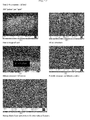
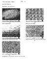
- Fig. 1 100 pulses per spot were delivered.
- SEMs scanning electron micrograms
- Image (a) shows a macro image of the substrate.
- Images (b) - (c) show the micro hillock structure having a height ⁇ 10 ⁇ m.
- Image (d) shows a periodic structure on the micro hillock structure which is barely visible.
- Image (e) shows nanoglobules having high sphericity. The polarization was 456 mV.
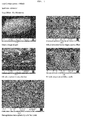
- Image (a) shows a macro image of the substrate. Images (b) - (c) show the micro hillock structure having a height > 10 ⁇ m. Image (d) shows a periodic structure on the micro hillock structure which is visible. Image (e) shows nanoglobules having sphericity with some tubular features. The polarization was 105 mV.
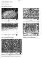
- Image (a) shows a macro image of the substrate.
- Images (b) - (c) show the micro hillock structure having a height ⁇ 25 ⁇ m.
- Image (d) shows a periodic structure on the micro hillock structure which is pronounced.
- Image (e) shows angular nanoglobules and large voids and cavities. The polarization was 45 mV.
- a series of cylindrical platinum electrodes having a diameter of 2.05 mm and an active length of 2.5 mm were processed on 30% of their surface via ultrafast laser texturing. Each of the cylinders was rotated on its axis head, translated via mechanical stages and a series of pulses were delivered. The sample was positioned under the laser while the laser impinged the surface at a nearly oblique angle. Variations in operating parameters give the indicated potential polarization results.
- a Rofin StarFrmto FX laser system was used for the exposure. The nominal spot size was varied at 50 ⁇ m, 100 ⁇ m and 200 ⁇ m. The offset step between spot centers was varied at 25 ⁇ m, 35 ⁇ m, 50 ⁇ m, 70 ⁇ m, and 140 ⁇ m between spot centers. The number of pulses per spot was 500. The desirable after potential polarization is ⁇ 5500 mV in this configuration due to the reduced processed surface size as compared to Example 1. In this Example 2, the laser exposure had a fixed wavelength of 800 nm.
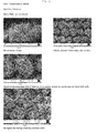
- spot size was 50 ⁇ m and the offset step was 35 ⁇ m.
- the scanning electron micrograms (SEMs) of Fig. 4 show the resulting structure.
- Image (a) shows a macro image of the substrate.
- Images (b) - (c) show the micro hillock structure of ⁇ 8 ⁇ m which corresponds to the offset step.
- Image (d) shows a periodic structure on the micro hillock structure.
- Image (e) shows angular nanoglobules with low sphericity. The polarization was 410 mV.
- spot size was 50 ⁇ m and the offset step was 35 ⁇ m x 25 ⁇ m.
- the scanning electron micrograms (SEMs) of Fig. 5 show the resulting structure.
- Image (a) shows a macro image of the substrate.
- Images (b) - (c) show the micro hillock structure of ⁇ 25 ⁇ m.
- Image (d) shows a periodic structure on the micro hillock walls.
- Image (e) shows angular nanoglobules with low sphericity and with large voids. The polarization was 365 mV.
- spot size was 50 ⁇ m and the offset step was 35 ⁇ m x 50 ⁇ m.
- the scanning electron micrograms (SEMs) of Fig. 6 show the resulting structure.
- Image (a) shows a macro image of the substrate.
- Images (b) - (c) show the micro hillock structure forms ridges due to offset. The hillock structure is very shallow.
- Image (d) shows a periodic structure on the micro hillock walls.
- Image (e) shows nanoglobules with sphericity and with few voids. The polarization was 490 mV.
- spot size was 50 ⁇ m and the offset step was 50 ⁇ m x 50 ⁇ m.
- the scanning electron micrograms (SEMs) of Fig. 7 show the resulting structure.
- Image (a) shows a macro image of the substrate.
- Images (b) - (c) show the micro hillock structure forms ridges due to offset. The hillock structure is very shallow.
- Image (d) shows a periodic structure on the micro hillock walls.
- Image (e) shows nanoglobules with a mixture and tubular structure. The polarization was 710 mV.
- spot size was 50 ⁇ m and the offset step was 250 ⁇ m x 25 ⁇ m.
- the scanning electron micrograms (SEMs) of Fig. 8 show the resulting structure.
- Image (a) shows a macro image of the substrate.
- Images (b) - (c) show the micro hillock structure forms ridges due to offset.
- the structure shows deep hillock features and some periodic structures can be seen on the hillock walls.
- Image (d) shows nanoglobules having sphericity and deep voids.
- the polarization was 185 mV.
- spot size was 100 ⁇ m and the offset step was 70 ⁇ m x 70 ⁇ m.
- the scanning electron micrograms (SEMs) of Fig. 9 show the resulting structure.
- Image (a) shows a macro image of the substrate.
- Images (b) - (c) show the hillock structure offset and hillock features proportional to offset.
- Image (d) shows a periodic structure on the micro hillock walls.
- Image (e) shows nanoglobules with a sphericity and few voids. The polarization was 525 mV.
- spot size was 200 ⁇ m and the offset step was 140 ⁇ m x 140 ⁇ m.
- the scanning electron micrograms (SEMs) of Fig. 10 show the resulting structure.
- Image (a) shows a macro image of the substrate.
- Images (b) - (c) show the hillock structure offset and hillock features proportional to offset.
- Image (d) shows a periodic structure on the micro hillock walls.
- Image (e) shows nanoglobules with a tubular structures and few voids. The polarization was 630 mV.
- the void width of the hillock structure is influenced by the laser spot size while the periodicity of the raised hillock structures is formed by the offset step.
- Similar patterns of nanoglobules such as in Trial C and Trial E gave very different results based upon a change in the macro-structured hillocks. It is preferred to have a series of raised structures with nanoglobules superimposed on those structures as in Trial E, as compared to a row of connected hillocks as in the case of Trial A and C. It is also preferred to have uniformly created mesa structures as in Trial E as compared to oblong structures as seen in Trial B.
- the nanoglobules are preferred to be in the form of spheres or angular globules which are well connect to the surface as compared to tubular structures such as in comparing Trial D to Trial F.
- the best performance also appears to come from nanoglobules structure with a high volume of voids such as in comparing Trial A to Trial D.
- the creation of the nanoglobules with a high volume of voids is influenced by the number of energy pulses in each individual spot as seen in Trials 1, 2 and 3.
Landscapes
- Health & Medical Sciences (AREA)
- Engineering & Computer Science (AREA)
- Animal Behavior & Ethology (AREA)
- Radiology & Medical Imaging (AREA)
- Veterinary Medicine (AREA)
- Public Health (AREA)
- General Health & Medical Sciences (AREA)
- Life Sciences & Earth Sciences (AREA)
- Biomedical Technology (AREA)
- Nuclear Medicine, Radiotherapy & Molecular Imaging (AREA)
- Physics & Mathematics (AREA)
- Plasma & Fusion (AREA)
- Optics & Photonics (AREA)
- Mechanical Engineering (AREA)
- Heart & Thoracic Surgery (AREA)
- Cardiology (AREA)
- Electrotherapy Devices (AREA)
Priority Applications (1)
| Application Number | Priority Date | Filing Date | Title |
|---|---|---|---|
| PL14192110T PL2886155T3 (pl) | 2013-12-20 | 2014-11-06 | Biomedyczna elektroda |
Applications Claiming Priority (1)
| Application Number | Priority Date | Filing Date | Title |
|---|---|---|---|
| US14/136,810 US9117680B2 (en) | 2013-12-20 | 2013-12-20 | Biomedical electrode |
Publications (2)
| Publication Number | Publication Date |
|---|---|
| EP2886155A1 true EP2886155A1 (fr) | 2015-06-24 |
| EP2886155B1 EP2886155B1 (fr) | 2018-01-03 |
Family
ID=51868070
Family Applications (1)
| Application Number | Title | Priority Date | Filing Date |
|---|---|---|---|
| EP14192110.6A Active EP2886155B1 (fr) | 2013-12-20 | 2014-11-06 | Électrode biomédicale |
Country Status (7)
| Country | Link |
|---|---|
| US (1) | US9117680B2 (fr) |
| EP (1) | EP2886155B1 (fr) |
| JP (1) | JP6494270B2 (fr) |
| AU (2) | AU2014277800A1 (fr) |
| CA (1) | CA2869873C (fr) |
| IL (1) | IL235503A0 (fr) |
| PL (1) | PL2886155T3 (fr) |
Cited By (1)
| Publication number | Priority date | Publication date | Assignee | Title |
|---|---|---|---|---|
| EP3108927A1 (fr) * | 2015-06-17 | 2016-12-28 | Pulse Technologies, Inc. | Électrode biomédicale présentant une faible teneur en oxygène |
Families Citing this family (11)
| Publication number | Priority date | Publication date | Assignee | Title |
|---|---|---|---|---|
| US9919502B2 (en) | 2014-04-23 | 2018-03-20 | Schaublin Sa | Method and apparatus for preparing a surface for bonding a material thereto |
| US11548092B2 (en) | 2018-03-19 | 2023-01-10 | Medtronic, Inc. | Surface texturing using energy pulses |
| KR102126464B1 (ko) * | 2018-05-04 | 2020-06-24 | 한국과학기술연구원 | 인체 이식형 센서 |
| EP3958774B1 (fr) | 2019-07-02 | 2023-08-16 | St. Jude Medical, Cardiology Division, Inc. | Conception d'électrode à impédance réduite |
| CN110693480B (zh) * | 2019-10-11 | 2022-04-08 | 哈尔滨工业大学 | 一种基于金属-mof微观形貌特征的可植入神经电极及其制备方法 |
| US12420103B1 (en) | 2020-08-20 | 2025-09-23 | Axonics, Inc. | Neurostimulation leads with reduced current leakage |
| US11495369B2 (en) | 2021-03-25 | 2022-11-08 | Heraeus Deutschland GmbH & Co. KG | Laser structured, coated electrical conductor and method for producing same |
| JP2024538136A (ja) * | 2021-10-12 | 2024-10-18 | パルス・アイピー・リミテッド・ライアビリティ・カンパニー | 改善された抗菌表面を有するデバイス |
| US11999013B2 (en) | 2021-12-29 | 2024-06-04 | PlasmaTex, LLC | Pulsed laser processing of medical devices |
| CN114602059B (zh) * | 2022-03-09 | 2025-03-25 | 清华大学 | 电极触点的加工方法及植入式电极 |
| WO2026002536A1 (fr) * | 2024-06-27 | 2026-01-02 | Biotronik Se & Co. Kg | Augmentation de la capacité de double couche de titane par génération laser d'une couche de nitrure de titane et nano-structuration et ablation laser en amont simultanées |
Citations (7)
| Publication number | Priority date | Publication date | Assignee | Title |
|---|---|---|---|---|
| US5318572A (en) | 1992-06-02 | 1994-06-07 | Siemens Pacesetter, Inc. | High efficiency tissue stimulating and signal sensing electrode |
| US5571158A (en) | 1991-08-06 | 1996-11-05 | Biotronik Mess- Und Therapiegeraete Gmbh & Co. Ingenieurbuero Berlin | Stimulation Electrode |
| US6799076B2 (en) | 1999-12-07 | 2004-09-28 | Greatbatch-Hittman, Inc. | Coated electrode and method of making a coated electrode |
| WO2007095549A2 (fr) * | 2006-02-13 | 2007-08-23 | Medtronic, Inc. | dispositifs medicaux ayant des surfaces texturees |
| US20080299289A1 (en) * | 2007-05-29 | 2008-12-04 | Fisk Andrew E | Optimum Surface Texture Geometry |
| US20110160821A1 (en) | 2009-12-30 | 2011-06-30 | Jackson Timothy R | Electrode surface modification for imparting current density directionality in lead electrodes |
| EP2808053A1 (fr) * | 2013-05-30 | 2014-12-03 | Pulse Technologies, Inc. | Électrode implantable biocompatible |
Family Cites Families (4)
| Publication number | Priority date | Publication date | Assignee | Title |
|---|---|---|---|---|
| US8948881B2 (en) * | 2006-05-19 | 2015-02-03 | Greatbatch Ltd. | Method for producing implantable electrode coatings with a plurality of morphologies |
| US8996129B2 (en) * | 2007-01-31 | 2015-03-31 | Medtronic, Inc. | Medical electrode including an iridium oxide surface and methods of fabrication |
| JP2012509140A (ja) * | 2008-11-20 | 2012-04-19 | カーディアック ペースメイカーズ, インコーポレイテッド | 構造化された表面を有する細胞反発性電極 |
| WO2012097879A1 (fr) * | 2011-01-21 | 2012-07-26 | St. Jude Medical Ab | Dispositif implantable avec caractéristiques de surface améliorées |
-
2013
- 2013-12-20 US US14/136,810 patent/US9117680B2/en active Active
-
2014
- 2014-10-31 CA CA2869873A patent/CA2869873C/fr active Active
- 2014-11-05 IL IL235503A patent/IL235503A0/en active IP Right Grant
- 2014-11-06 EP EP14192110.6A patent/EP2886155B1/fr active Active
- 2014-11-06 PL PL14192110T patent/PL2886155T3/pl unknown
- 2014-12-18 JP JP2014255717A patent/JP6494270B2/ja active Active
- 2014-12-19 AU AU2014277800A patent/AU2014277800A1/en not_active Abandoned
-
2020
- 2020-04-02 AU AU2020202344A patent/AU2020202344B2/en active Active
Patent Citations (7)
| Publication number | Priority date | Publication date | Assignee | Title |
|---|---|---|---|---|
| US5571158A (en) | 1991-08-06 | 1996-11-05 | Biotronik Mess- Und Therapiegeraete Gmbh & Co. Ingenieurbuero Berlin | Stimulation Electrode |
| US5318572A (en) | 1992-06-02 | 1994-06-07 | Siemens Pacesetter, Inc. | High efficiency tissue stimulating and signal sensing electrode |
| US6799076B2 (en) | 1999-12-07 | 2004-09-28 | Greatbatch-Hittman, Inc. | Coated electrode and method of making a coated electrode |
| WO2007095549A2 (fr) * | 2006-02-13 | 2007-08-23 | Medtronic, Inc. | dispositifs medicaux ayant des surfaces texturees |
| US20080299289A1 (en) * | 2007-05-29 | 2008-12-04 | Fisk Andrew E | Optimum Surface Texture Geometry |
| US20110160821A1 (en) | 2009-12-30 | 2011-06-30 | Jackson Timothy R | Electrode surface modification for imparting current density directionality in lead electrodes |
| EP2808053A1 (fr) * | 2013-05-30 | 2014-12-03 | Pulse Technologies, Inc. | Électrode implantable biocompatible |
Cited By (2)
| Publication number | Priority date | Publication date | Assignee | Title |
|---|---|---|---|---|
| EP3108927A1 (fr) * | 2015-06-17 | 2016-12-28 | Pulse Technologies, Inc. | Électrode biomédicale présentant une faible teneur en oxygène |
| EP4714489A1 (fr) * | 2015-06-17 | 2026-03-25 | Pulse IP, LLC | Electrode biomedicale a faible teneur en oxygene |
Also Published As
| Publication number | Publication date |
|---|---|
| CA2869873A1 (fr) | 2015-06-20 |
| US9117680B2 (en) | 2015-08-25 |
| IL235503A0 (en) | 2015-01-29 |
| CA2869873C (fr) | 2021-06-01 |
| EP2886155B1 (fr) | 2018-01-03 |
| AU2020202344A1 (en) | 2020-04-23 |
| AU2014277800A1 (en) | 2015-07-09 |
| US20150173635A1 (en) | 2015-06-25 |
| AU2020202344B2 (en) | 2021-12-16 |
| JP2015119969A (ja) | 2015-07-02 |
| JP6494270B2 (ja) | 2019-04-03 |
| PL2886155T3 (pl) | 2018-08-31 |
Similar Documents
| Publication | Publication Date | Title |
|---|---|---|
| AU2020202344B2 (en) | Biomedical electrode | |
| US20240215885A1 (en) | Biocompatible implantable electrode | |
| AU2021201430B2 (en) | Biomedical electrode having low oxygen content | |
| US20210370053A1 (en) | Neuro-stimulation and Sensor Devices Comprising Low-Impedance Electrodes, and Methods, Systems And Uses Thereof | |
| EP2736402B1 (fr) | Dispositif optoélectrique et procédé de réduction d'artéfacts | |
| Frederick et al. | Activated iridium oxide film (AIROF) electrodes for neural tissue stimulation | |
| JP5313255B2 (ja) | 最適表面組織形状 | |
| Leber et al. | Different methods to alter surface morphology of high aspect ratio structures | |
| Bhandari et al. | A novel masking method for high aspect ratio penetrating microelectrode arrays | |
| US20160059353A1 (en) | Surface structuring of metals | |
| US11495369B2 (en) | Laser structured, coated electrical conductor and method for producing same | |
| CN114602059B (zh) | 电极触点的加工方法及植入式电极 | |
| US12403300B2 (en) | Electrode for a medical device | |
| WO2026002536A1 (fr) | Augmentation de la capacité de double couche de titane par génération laser d'une couche de nitrure de titane et nano-structuration et ablation laser en amont simultanées |
Legal Events
| Date | Code | Title | Description |
|---|---|---|---|
| PUAI | Public reference made under article 153(3) epc to a published international application that has entered the european phase |
Free format text: ORIGINAL CODE: 0009012 |
|
| 17P | Request for examination filed |
Effective date: 20141106 |
|
| AK | Designated contracting states |
Kind code of ref document: A1 Designated state(s): AL AT BE BG CH CY CZ DE DK EE ES FI FR GB GR HR HU IE IS IT LI LT LU LV MC MK MT NL NO PL PT RO RS SE SI SK SM TR |
|
| AX | Request for extension of the european patent |
Extension state: BA ME |
|
| R17P | Request for examination filed (corrected) |
Effective date: 20151222 |
|
| RBV | Designated contracting states (corrected) |
Designated state(s): AL AT BE BG CH CY CZ DE DK EE ES FI FR GB GR HR HU IE IS IT LI LT LU LV MC MK MT NL NO PL PT RO RS SE SI SK SM TR |
|
| RIC1 | Information provided on ipc code assigned before grant |
Ipc: A61N 1/05 20060101ALN20170330BHEP Ipc: B82Y 40/00 20110101ALN20170330BHEP Ipc: A61N 1/04 20060101AFI20170330BHEP Ipc: B82Y 5/00 20110101ALN20170330BHEP Ipc: A61B 5/042 20060101ALN20170330BHEP Ipc: A61B 5/04 20060101ALI20170330BHEP Ipc: B82Y 30/00 20110101ALN20170330BHEP |
|
| GRAP | Despatch of communication of intention to grant a patent |
Free format text: ORIGINAL CODE: EPIDOSNIGR1 |
|
| RIC1 | Information provided on ipc code assigned before grant |
Ipc: A61B 5/042 20060101ALN20170425BHEP Ipc: A61B 5/04 20060101ALI20170425BHEP Ipc: A61N 1/05 20060101ALN20170425BHEP Ipc: A61N 1/04 20060101AFI20170425BHEP Ipc: B82Y 30/00 20110101ALN20170425BHEP Ipc: B82Y 40/00 20110101ALN20170425BHEP Ipc: B82Y 5/00 20110101ALN20170425BHEP |
|
| INTG | Intention to grant announced |
Effective date: 20170516 |
|
| RIN1 | Information on inventor provided before grant (corrected) |
Inventor name: FISK, ANDREW E. |
|
| GRAS | Grant fee paid |
Free format text: ORIGINAL CODE: EPIDOSNIGR3 |
|
| GRAA | (expected) grant |
Free format text: ORIGINAL CODE: 0009210 |
|
| AK | Designated contracting states |
Kind code of ref document: B1 Designated state(s): AL AT BE BG CH CY CZ DE DK EE ES FI FR GB GR HR HU IE IS IT LI LT LU LV MC MK MT NL NO PL PT RO RS SE SI SK SM TR |
|
| REG | Reference to a national code |
Ref country code: GB Ref legal event code: FG4D |
|
| REG | Reference to a national code |
Ref country code: CH Ref legal event code: EP Ref country code: AT Ref legal event code: REF Ref document number: 959672 Country of ref document: AT Kind code of ref document: T Effective date: 20180115 |
|
| REG | Reference to a national code |
Ref country code: IE Ref legal event code: FG4D |
|
| REG | Reference to a national code |
Ref country code: DE Ref legal event code: R096 Ref document number: 602014019314 Country of ref document: DE |
|
| REG | Reference to a national code |
Ref country code: SE Ref legal event code: TRGR |
|
| REG | Reference to a national code |
Ref country code: NL Ref legal event code: FP |
|
| REG | Reference to a national code |
Ref country code: LT Ref legal event code: MG4D |
|
| REG | Reference to a national code |
Ref country code: CH Ref legal event code: NV Representative=s name: RIEDERER HASLER AND PARTNER PATENTANWAELTE AG, CH |
|
| PG25 | Lapsed in a contracting state [announced via postgrant information from national office to epo] |
Ref country code: NO Free format text: LAPSE BECAUSE OF FAILURE TO SUBMIT A TRANSLATION OF THE DESCRIPTION OR TO PAY THE FEE WITHIN THE PRESCRIBED TIME-LIMIT Effective date: 20180403 Ref country code: FI Free format text: LAPSE BECAUSE OF FAILURE TO SUBMIT A TRANSLATION OF THE DESCRIPTION OR TO PAY THE FEE WITHIN THE PRESCRIBED TIME-LIMIT Effective date: 20180103 Ref country code: CY Free format text: LAPSE BECAUSE OF FAILURE TO SUBMIT A TRANSLATION OF THE DESCRIPTION OR TO PAY THE FEE WITHIN THE PRESCRIBED TIME-LIMIT Effective date: 20180103 Ref country code: ES Free format text: LAPSE BECAUSE OF FAILURE TO SUBMIT A TRANSLATION OF THE DESCRIPTION OR TO PAY THE FEE WITHIN THE PRESCRIBED TIME-LIMIT Effective date: 20180103 Ref country code: HR Free format text: LAPSE BECAUSE OF FAILURE TO SUBMIT A TRANSLATION OF THE DESCRIPTION OR TO PAY THE FEE WITHIN THE PRESCRIBED TIME-LIMIT Effective date: 20180103 Ref country code: LT Free format text: LAPSE BECAUSE OF FAILURE TO SUBMIT A TRANSLATION OF THE DESCRIPTION OR TO PAY THE FEE WITHIN THE PRESCRIBED TIME-LIMIT Effective date: 20180103 |
|
| PG25 | Lapsed in a contracting state [announced via postgrant information from national office to epo] |
Ref country code: GR Free format text: LAPSE BECAUSE OF FAILURE TO SUBMIT A TRANSLATION OF THE DESCRIPTION OR TO PAY THE FEE WITHIN THE PRESCRIBED TIME-LIMIT Effective date: 20180404 Ref country code: RS Free format text: LAPSE BECAUSE OF FAILURE TO SUBMIT A TRANSLATION OF THE DESCRIPTION OR TO PAY THE FEE WITHIN THE PRESCRIBED TIME-LIMIT Effective date: 20180103 Ref country code: BG Free format text: LAPSE BECAUSE OF FAILURE TO SUBMIT A TRANSLATION OF THE DESCRIPTION OR TO PAY THE FEE WITHIN THE PRESCRIBED TIME-LIMIT Effective date: 20180403 Ref country code: IS Free format text: LAPSE BECAUSE OF FAILURE TO SUBMIT A TRANSLATION OF THE DESCRIPTION OR TO PAY THE FEE WITHIN THE PRESCRIBED TIME-LIMIT Effective date: 20180503 Ref country code: LV Free format text: LAPSE BECAUSE OF FAILURE TO SUBMIT A TRANSLATION OF THE DESCRIPTION OR TO PAY THE FEE WITHIN THE PRESCRIBED TIME-LIMIT Effective date: 20180103 |
|
| REG | Reference to a national code |
Ref country code: DE Ref legal event code: R097 Ref document number: 602014019314 Country of ref document: DE |
|
| PG25 | Lapsed in a contracting state [announced via postgrant information from national office to epo] |
Ref country code: EE Free format text: LAPSE BECAUSE OF FAILURE TO SUBMIT A TRANSLATION OF THE DESCRIPTION OR TO PAY THE FEE WITHIN THE PRESCRIBED TIME-LIMIT Effective date: 20180103 Ref country code: RO Free format text: LAPSE BECAUSE OF FAILURE TO SUBMIT A TRANSLATION OF THE DESCRIPTION OR TO PAY THE FEE WITHIN THE PRESCRIBED TIME-LIMIT Effective date: 20180103 Ref country code: AL Free format text: LAPSE BECAUSE OF FAILURE TO SUBMIT A TRANSLATION OF THE DESCRIPTION OR TO PAY THE FEE WITHIN THE PRESCRIBED TIME-LIMIT Effective date: 20180103 |
|
| PLBE | No opposition filed within time limit |
Free format text: ORIGINAL CODE: 0009261 |
|
| STAA | Information on the status of an ep patent application or granted ep patent |
Free format text: STATUS: NO OPPOSITION FILED WITHIN TIME LIMIT |
|
| PG25 | Lapsed in a contracting state [announced via postgrant information from national office to epo] |
Ref country code: SK Free format text: LAPSE BECAUSE OF FAILURE TO SUBMIT A TRANSLATION OF THE DESCRIPTION OR TO PAY THE FEE WITHIN THE PRESCRIBED TIME-LIMIT Effective date: 20180103 Ref country code: DK Free format text: LAPSE BECAUSE OF FAILURE TO SUBMIT A TRANSLATION OF THE DESCRIPTION OR TO PAY THE FEE WITHIN THE PRESCRIBED TIME-LIMIT Effective date: 20180103 Ref country code: SM Free format text: LAPSE BECAUSE OF FAILURE TO SUBMIT A TRANSLATION OF THE DESCRIPTION OR TO PAY THE FEE WITHIN THE PRESCRIBED TIME-LIMIT Effective date: 20180103 |
|
| RAP2 | Party data changed (patent owner data changed or rights of a patent transferred) |
Owner name: PULSE IP, LLC |
|
| REG | Reference to a national code |
Ref country code: DE Ref legal event code: R082 Ref document number: 602014019314 Country of ref document: DE Representative=s name: SSM SANDMAIR PATENTANWAELTE RECHTSANWALT PARTN, DE Ref country code: DE Ref legal event code: R081 Ref document number: 602014019314 Country of ref document: DE Owner name: PULSE IP, LLC, QUAKERTOWN, US Free format text: FORMER OWNER: PULSE TECHNOLOGIES, INC., QUAKERTOWN, PA, US |
|
| 26N | No opposition filed |
Effective date: 20181005 |
|
| REG | Reference to a national code |
Ref country code: GB Ref legal event code: 732E Free format text: REGISTERED BETWEEN 20181206 AND 20181212 |
|
| REG | Reference to a national code |
Ref country code: CH Ref legal event code: PUE Owner name: PULSE IP, LLC, US Free format text: FORMER OWNER: PULSE TECHNOLOGIES, INC., US |
|
| PG25 | Lapsed in a contracting state [announced via postgrant information from national office to epo] |
Ref country code: SI Free format text: LAPSE BECAUSE OF FAILURE TO SUBMIT A TRANSLATION OF THE DESCRIPTION OR TO PAY THE FEE WITHIN THE PRESCRIBED TIME-LIMIT Effective date: 20180103 |
|
| REG | Reference to a national code |
Ref country code: NL Ref legal event code: PD Owner name: PULSE IP, LLC; US Free format text: DETAILS ASSIGNMENT: CHANGE OF OWNER(S), ASSIGNMENT; FORMER OWNER NAME: PULSE TECHNOLOGIES, INC. Effective date: 20190107 |
|
| REG | Reference to a national code |
Ref country code: AT Ref legal event code: PC Ref document number: 959672 Country of ref document: AT Kind code of ref document: T Owner name: PULSE IP, LLC, US Effective date: 20190403 |
|
| REG | Reference to a national code |
Ref country code: AT Ref legal event code: UEP Ref document number: 959672 Country of ref document: AT Kind code of ref document: T Effective date: 20180103 |
|
| PG25 | Lapsed in a contracting state [announced via postgrant information from national office to epo] |
Ref country code: MC Free format text: LAPSE BECAUSE OF FAILURE TO SUBMIT A TRANSLATION OF THE DESCRIPTION OR TO PAY THE FEE WITHIN THE PRESCRIBED TIME-LIMIT Effective date: 20180103 Ref country code: LU Free format text: LAPSE BECAUSE OF NON-PAYMENT OF DUE FEES Effective date: 20181106 |
|
| REG | Reference to a national code |
Ref country code: BE Ref legal event code: MM Effective date: 20181130 |
|
| PG25 | Lapsed in a contracting state [announced via postgrant information from national office to epo] |
Ref country code: BE Free format text: LAPSE BECAUSE OF NON-PAYMENT OF DUE FEES Effective date: 20181130 |
|
| PG25 | Lapsed in a contracting state [announced via postgrant information from national office to epo] |
Ref country code: MT Free format text: LAPSE BECAUSE OF NON-PAYMENT OF DUE FEES Effective date: 20181106 |
|
| PG25 | Lapsed in a contracting state [announced via postgrant information from national office to epo] |
Ref country code: TR Free format text: LAPSE BECAUSE OF FAILURE TO SUBMIT A TRANSLATION OF THE DESCRIPTION OR TO PAY THE FEE WITHIN THE PRESCRIBED TIME-LIMIT Effective date: 20180103 |
|
| PG25 | Lapsed in a contracting state [announced via postgrant information from national office to epo] |
Ref country code: PT Free format text: LAPSE BECAUSE OF FAILURE TO SUBMIT A TRANSLATION OF THE DESCRIPTION OR TO PAY THE FEE WITHIN THE PRESCRIBED TIME-LIMIT Effective date: 20180103 |
|
| PG25 | Lapsed in a contracting state [announced via postgrant information from national office to epo] |
Ref country code: MK Free format text: LAPSE BECAUSE OF NON-PAYMENT OF DUE FEES Effective date: 20180103 Ref country code: HU Free format text: LAPSE BECAUSE OF FAILURE TO SUBMIT A TRANSLATION OF THE DESCRIPTION OR TO PAY THE FEE WITHIN THE PRESCRIBED TIME-LIMIT; INVALID AB INITIO Effective date: 20141106 |
|
| PGFP | Annual fee paid to national office [announced via postgrant information from national office to epo] |
Ref country code: NL Payment date: 20250912 Year of fee payment: 12 Ref country code: PL Payment date: 20250829 Year of fee payment: 12 |
|
| PGFP | Annual fee paid to national office [announced via postgrant information from national office to epo] |
Ref country code: GB Payment date: 20250918 Year of fee payment: 12 |
|
| PGFP | Annual fee paid to national office [announced via postgrant information from national office to epo] |
Ref country code: FR Payment date: 20250908 Year of fee payment: 12 |
|
| PGFP | Annual fee paid to national office [announced via postgrant information from national office to epo] |
Ref country code: SE Payment date: 20250910 Year of fee payment: 12 |
|
| PGFP | Annual fee paid to national office [announced via postgrant information from national office to epo] |
Ref country code: IE Payment date: 20250909 Year of fee payment: 12 |
|
| REG | Reference to a national code |
Ref country code: CH Ref legal event code: U11 Free format text: ST27 STATUS EVENT CODE: U-0-0-U10-U11 (AS PROVIDED BY THE NATIONAL OFFICE) Effective date: 20251201 |
|
| PGFP | Annual fee paid to national office [announced via postgrant information from national office to epo] |
Ref country code: DE Payment date: 20250910 Year of fee payment: 12 |
|
| PGFP | Annual fee paid to national office [announced via postgrant information from national office to epo] |
Ref country code: AT Payment date: 20251027 Year of fee payment: 12 |
|
| PGFP | Annual fee paid to national office [announced via postgrant information from national office to epo] |
Ref country code: IT Payment date: 20251022 Year of fee payment: 12 |
|
| PGFP | Annual fee paid to national office [announced via postgrant information from national office to epo] |
Ref country code: CH Payment date: 20251201 Year of fee payment: 12 |
|
| PGFP | Annual fee paid to national office [announced via postgrant information from national office to epo] |
Ref country code: CZ Payment date: 20251021 Year of fee payment: 12 |