EP2886244A1 - Procédé de fixation d'un composant sur un substrat - Google Patents
Procédé de fixation d'un composant sur un substrat Download PDFInfo
- Publication number
- EP2886244A1 EP2886244A1 EP13197640.9A EP13197640A EP2886244A1 EP 2886244 A1 EP2886244 A1 EP 2886244A1 EP 13197640 A EP13197640 A EP 13197640A EP 2886244 A1 EP2886244 A1 EP 2886244A1
- Authority
- EP
- European Patent Office
- Prior art keywords
- solder
- component
- flux
- substrate
- dicarboxylic acid
- Prior art date
- Legal status (The legal status is an assumption and is not a legal conclusion. Google has not performed a legal analysis and makes no representation as to the accuracy of the status listed.)
- Withdrawn
Links
Images

Classifications
-
- H—ELECTRICITY
- H05—ELECTRIC TECHNIQUES NOT OTHERWISE PROVIDED FOR
- H05K—PRINTED CIRCUITS; CASINGS OR CONSTRUCTIONAL DETAILS OF ELECTRIC APPARATUS; MANUFACTURE OF ASSEMBLAGES OF ELECTRICAL COMPONENTS
- H05K3/00—Apparatus or processes for manufacturing printed circuits
- H05K3/30—Assembling printed circuits with electric components, e.g. with resistors
- H05K3/32—Assembling printed circuits with electric components, e.g. with resistors electrically connecting electric components or wires to printed circuits
- H05K3/34—Assembling printed circuits with electric components, e.g. with resistors electrically connecting electric components or wires to printed circuits by soldering
- H05K3/341—Surface mounted components
- H05K3/3431—Leadless components
- H05K3/3436—Leadless components having an array of bottom contacts, e.g. pad grid array or ball grid array components
-
- B—PERFORMING OPERATIONS; TRANSPORTING
- B23—MACHINE TOOLS; METAL-WORKING NOT OTHERWISE PROVIDED FOR
- B23K—SOLDERING OR UNSOLDERING; WELDING; CLADDING OR PLATING BY SOLDERING OR WELDING; CUTTING BY APPLYING HEAT LOCALLY, e.g. FLAME CUTTING; WORKING BY LASER BEAM
- B23K1/00—Soldering, e.g. brazing, or unsoldering
- B23K1/0008—Soldering, e.g. brazing, or unsoldering specially adapted for particular articles or work
- B23K1/0016—Soldering of electronic components
-
- B—PERFORMING OPERATIONS; TRANSPORTING
- B23—MACHINE TOOLS; METAL-WORKING NOT OTHERWISE PROVIDED FOR
- B23K—SOLDERING OR UNSOLDERING; WELDING; CLADDING OR PLATING BY SOLDERING OR WELDING; CUTTING BY APPLYING HEAT LOCALLY, e.g. FLAME CUTTING; WORKING BY LASER BEAM
- B23K35/00—Rods, electrodes, materials, or media, for use in soldering, welding, or cutting
- B23K35/02—Rods, electrodes, materials, or media, for use in soldering, welding, or cutting characterised by mechanical features, e.g. shape
- B23K35/0222—Rods, electrodes, materials, or media, for use in soldering, welding, or cutting characterised by mechanical features, e.g. shape for use in soldering or brazing
- B23K35/0244—Powders, particles or spheres; Preforms made therefrom
- B23K35/025—Pastes, creams or slurries
-
- B—PERFORMING OPERATIONS; TRANSPORTING
- B23—MACHINE TOOLS; METAL-WORKING NOT OTHERWISE PROVIDED FOR
- B23K—SOLDERING OR UNSOLDERING; WELDING; CLADDING OR PLATING BY SOLDERING OR WELDING; CUTTING BY APPLYING HEAT LOCALLY, e.g. FLAME CUTTING; WORKING BY LASER BEAM
- B23K35/00—Rods, electrodes, materials, or media, for use in soldering, welding, or cutting
- B23K35/22—Rods, electrodes, materials, or media, for use in soldering, welding, or cutting characterised by the composition or nature of the material
- B23K35/24—Selection of soldering or welding materials proper
- B23K35/26—Selection of soldering or welding materials proper with the principal constituent melting at less than 400°C
- B23K35/262—Sn as the principal constituent
-
- B—PERFORMING OPERATIONS; TRANSPORTING
- B23—MACHINE TOOLS; METAL-WORKING NOT OTHERWISE PROVIDED FOR
- B23K—SOLDERING OR UNSOLDERING; WELDING; CLADDING OR PLATING BY SOLDERING OR WELDING; CUTTING BY APPLYING HEAT LOCALLY, e.g. FLAME CUTTING; WORKING BY LASER BEAM
- B23K35/00—Rods, electrodes, materials, or media, for use in soldering, welding, or cutting
- B23K35/22—Rods, electrodes, materials, or media, for use in soldering, welding, or cutting characterised by the composition or nature of the material
- B23K35/36—Selection of non-metallic compositions, e.g. coatings or fluxes; Selection of soldering or welding materials, conjoint with selection of non-metallic compositions, both selections being of interest
- B23K35/3612—Selection of non-metallic compositions, e.g. coatings or fluxes; Selection of soldering or welding materials, conjoint with selection of non-metallic compositions, both selections being of interest with organic compounds as principal constituents
- B23K35/3615—N-compounds
-
- B—PERFORMING OPERATIONS; TRANSPORTING
- B23—MACHINE TOOLS; METAL-WORKING NOT OTHERWISE PROVIDED FOR
- B23K—SOLDERING OR UNSOLDERING; WELDING; CLADDING OR PLATING BY SOLDERING OR WELDING; CUTTING BY APPLYING HEAT LOCALLY, e.g. FLAME CUTTING; WORKING BY LASER BEAM
- B23K35/00—Rods, electrodes, materials, or media, for use in soldering, welding, or cutting
- B23K35/22—Rods, electrodes, materials, or media, for use in soldering, welding, or cutting characterised by the composition or nature of the material
- B23K35/36—Selection of non-metallic compositions, e.g. coatings or fluxes; Selection of soldering or welding materials, conjoint with selection of non-metallic compositions, both selections being of interest
- B23K35/3612—Selection of non-metallic compositions, e.g. coatings or fluxes; Selection of soldering or welding materials, conjoint with selection of non-metallic compositions, both selections being of interest with organic compounds as principal constituents
- B23K35/3618—Carboxylic acids or salts
-
- B—PERFORMING OPERATIONS; TRANSPORTING
- B23—MACHINE TOOLS; METAL-WORKING NOT OTHERWISE PROVIDED FOR
- B23K—SOLDERING OR UNSOLDERING; WELDING; CLADDING OR PLATING BY SOLDERING OR WELDING; CUTTING BY APPLYING HEAT LOCALLY, e.g. FLAME CUTTING; WORKING BY LASER BEAM
- B23K35/00—Rods, electrodes, materials, or media, for use in soldering, welding, or cutting
- B23K35/22—Rods, electrodes, materials, or media, for use in soldering, welding, or cutting characterised by the composition or nature of the material
- B23K35/36—Selection of non-metallic compositions, e.g. coatings or fluxes; Selection of soldering or welding materials, conjoint with selection of non-metallic compositions, both selections being of interest
- B23K35/362—Selection of compositions of fluxes
-
- H—ELECTRICITY
- H05—ELECTRIC TECHNIQUES NOT OTHERWISE PROVIDED FOR
- H05K—PRINTED CIRCUITS; CASINGS OR CONSTRUCTIONAL DETAILS OF ELECTRIC APPARATUS; MANUFACTURE OF ASSEMBLAGES OF ELECTRICAL COMPONENTS
- H05K3/00—Apparatus or processes for manufacturing printed circuits
- H05K3/30—Assembling printed circuits with electric components, e.g. with resistors
- H05K3/32—Assembling printed circuits with electric components, e.g. with resistors electrically connecting electric components or wires to printed circuits
- H05K3/34—Assembling printed circuits with electric components, e.g. with resistors electrically connecting electric components or wires to printed circuits by soldering
- H05K3/346—Solder materials or compositions specially adapted therefor
-
- H—ELECTRICITY
- H05—ELECTRIC TECHNIQUES NOT OTHERWISE PROVIDED FOR
- H05K—PRINTED CIRCUITS; CASINGS OR CONSTRUCTIONAL DETAILS OF ELECTRIC APPARATUS; MANUFACTURE OF ASSEMBLAGES OF ELECTRICAL COMPONENTS
- H05K3/00—Apparatus or processes for manufacturing printed circuits
- H05K3/30—Assembling printed circuits with electric components, e.g. with resistors
- H05K3/32—Assembling printed circuits with electric components, e.g. with resistors electrically connecting electric components or wires to printed circuits
- H05K3/34—Assembling printed circuits with electric components, e.g. with resistors electrically connecting electric components or wires to printed circuits by soldering
- H05K3/3489—Composition of fluxes; Application thereof; Other processes of activating the contact surfaces
-
- H—ELECTRICITY
- H05—ELECTRIC TECHNIQUES NOT OTHERWISE PROVIDED FOR
- H05K—PRINTED CIRCUITS; CASINGS OR CONSTRUCTIONAL DETAILS OF ELECTRIC APPARATUS; MANUFACTURE OF ASSEMBLAGES OF ELECTRICAL COMPONENTS
- H05K3/00—Apparatus or processes for manufacturing printed circuits
- H05K3/30—Assembling printed circuits with electric components, e.g. with resistors
- H05K3/32—Assembling printed circuits with electric components, e.g. with resistors electrically connecting electric components or wires to printed circuits
- H05K3/34—Assembling printed circuits with electric components, e.g. with resistors electrically connecting electric components or wires to printed circuits by soldering
- H05K3/341—Surface mounted components
Definitions
- the present invention relates to a method for mounting an electronic component on a substrate using a solder paste comprising a mixture of organic dicarboxylic acids and in which the thickness of the solder deposit is 25 to 200 ⁇ m.
- solder pastes are mainly used in the manufacture of integral circuits, such as in the semiconductor industry.
- electronic components are applied to substrates, such as circuit boards, and mechanically, electronically and thermally connected to them by means of a solder paste. Consequently, the demands placed on such a process and the solder pastes employed therein are manifold, especially considering an automated process.
- the surface of the substrate is provided with a solder paste, via which the contact with the component is produced. By heating the solder paste, the mechanical contact is strengthened.
- the solder paste can also serve to establish electrical contact between the component and the substrate and / or to dissipate the heat generated during operation of the component.
- WO 02/20211 A1 describes a solder for use in diffusion soldering processes, which comprises a mixture of at least partially metallized grains of a refractory metal and a solder metal, which differ by their melting temperature.
- US 5,672,542 relates to a method and a process for the application of electrically conductive substances to a substrate by means of solder balls, wherein the solder balls have a maximum distance of 400 microns to each other.
- a particular challenge in these methods are electronic components which, in addition to electrical connection points, also have thermal connection points On the bottom have, such as QFP components (Quad Flat Package), which have electrical connection points in the form of so-called legs, which are attached to the sides of the component and through which the electrical contact between the component and the substrate is made have, and a thermal interface on the bottom, which serves to dissipate the heat generated during operation of the component.
- QFP components Quad Flat Package
- the contacting of the connection points with the substrate takes place in each case with the aid of different solder pastes, one for the thermal and one for the electrical connection. It may happen that the introduced solder depot of the thermal connection points runs during heating.
- solder powder particles usually in the form of so-called solder balls, expelled in the direction of the electrical connection points and can lead to short circuits there. This is especially problematic if due to the predetermined distance between the component and substrate, for example via the electrical connection points, a corresponding amount of solder paste must be used so that it comes to a mutual contact.
- Flowing out in the context of the present invention is the leakage of the solder paste for the thermal connection between the component and the substrate beyond the delimitations of the thermal connection point of the component and / or substrate as well as the formation of unwanted solder balls when the solder paste is heated under process conditions, so that it to a contact between the solder paste and the electrical connection points of the component and thus leads to short circuits, to understand.
- solder paste comprising a solder and a flux, in particular a flux having a mixture of two different dicarboxylic acids
- the outflow of the solder paste and the formation of unwanted solder balls, and thus of short circuits to the electrical connection points of the component can be prevented.
- the thickness of the solder deposit between the component and the substrate decisively controls the outflow.
- solder deposit An essential component of the method is the solder deposit, which is described in more detail below.
- the solder deposit is formed from a solder paste, which is composed of a flux and a solder.
- the individual components of the solder paste are detailed below.
- the flux is an important component of the solder paste and determines, above all, its rheological properties. It has surprisingly been found that the occurrence of short circuits in the attachment of a component to a substrate can be reduced if a flux is used which comprises a mixture of two different dicarboxylic acids. It has been found that by using a solder paste which has said flux, a stable mechanical and thermal connection between the component and the substrate is formed without electrical short circuits occurring, and that the solder paste simultaneously has good processability and good wetting properties. In particular, in the interaction of the solder paste with a defined depot thickness in the range of 25 to 200 microns, show excellent properties.
- dicarboxylic acid A has 5 or more carbon atoms, preferably 6 to 8 carbon atoms and in particular 6 carbon atoms.
- dicarboxylic acid A is adipic acid.
- a dicarboxylic acid B is used as a further component, which has fewer carbon atoms than dicarboxylic acid A.
- dicarboxylic acid B has 4 or fewer carbon atoms, in particular 2 carbon atoms. Particularly preferred is an embodiment in the dicarboxylic acid B is oxalic acid. It has furthermore been found, surprisingly, that the advantageous effects occur in particular when dicarboxylic acid A and dicarboxylic acid B are present in a specific weight ratio to one another.
- the weight ratio of dicarboxylic acid A to dicarboxylic acid B is therefore 30: 1 to 5: 1, preferably 25: 1 to 7: 1, in particular 20: 1 to 10: 1.
- the flux dicarboxylic acid A in an amount of 7 to 13 wt .-%, preferably 8 to 12 wt .-%, each based on the total weight of the flux having.
- the flux is dicarboxylic acid B in an amount of 0.3 to 2.0 wt%, preferably 0.4 to 1.5 wt%, more preferably 0.45 to 1 , 0 wt .-%, each based on the total weight of the flux having.
- Amine component X is a diamine which has at least one tertiary amino group, preferably two tertiary amino groups.
- amine component X is selected from the group consisting of 1,2-tetramethylethylenediamine, 1,2-tetraethylethylenediamine and 1,2-tetrapropylethylenediamine, for example 1,2-tetra-n-propylethylenediamine and 1,2- Tetra-iso-propylethylenediamine.
- Particularly preferred are those diamines in which each tertiary amino group has two identical substituents.
- Tertiary amine in the context of the present invention is an amine whose nitrogen atom carries three carbon-containing substituents.
- Amine Component Y is a diamine or polyamine in which at least 2 of the amino groups are separated by at least 3 carbon atoms and which have at least 4 carbon atoms.
- Amine Component Y is a diamine in which the two amino groups are separated by at least 3 carbon atoms and which has at least 4 carbon atoms.
- amine component Y is a polyamine in which at least 2 of the amino groups are separated by at least 3 carbon atoms and which has at least 4 carbon atoms.
- amine component Y therefore has at least one primary amino group.
- amine component Y is selected from the group consisting of N-coco-1,3-diaminopropane, 1,6-diaminohexane, 1,7-diaminoheptane, 1,8-diaminooctane, 1,9-diaminononane and 1 , 10-diaminodecane.
- the amine to be used that is, amine component X or amine component Y, has no tertiary and / or quaternary carbon atoms.
- the amine has at least 6 carbon atoms.
- the carbon atoms may be present as a linking chain between two amino groups or may be bonded thereto as substituents of the nitrogen atoms.
- the total amount of amine, ie amine component A and / or amine component B in the flux is 2% by weight or less, preferably 1% by weight or less, for example 0.1% by weight to 2.0% by weight .-%, in each case based on the total weight of the flux.
- the amount of amine in the flux is preferably chosen so that a good processability of the solder paste and a good wetting of the surfaces of the component to be fastened and the substrate are ensured.
- the flux is amine component X and / or amine component Y in an amount of 0.1 to 2.0 wt .-%, preferably from 0.4 to 1.0 wt .-%, each based on the total weight of the flux.
- the flux additionally comprises monoamine.
- the monoamine is present in addition to the amine component X and / or the amine component Y.
- the monoamine is a secondary and / or tertiary monoamine. Therefore, an embodiment is preferred in which the monoamine is selected from the group consisting of secondary monoamine and tertiary monoamine and mixtures thereof. Most preferably, the monoamine is a tertiary monoamine.
- the flux comprises monoamine in an amount of from 0.5 to 5.5% by weight, preferably from 1.0 to 5.0% by weight, based in each case on the total weight of the flux.
- the flux has, in addition to the dicarboxylic acids A and B, further dicarboxylic acids which are different from the dicarboxylic acids A and B.
- the flux additionally contains dicarboxylic acids other than dicarboxylic acid A and dicarboxylic acid B in an amount of 0 to 2% by weight, preferably in an amount of 0.01 to 1.0% by weight. %, in each case based on the total weight of the flux.
- the total amount of all dicarboxylic acids in the flux is at most 15% by weight, preferably 7 to 13% by weight, in particular 8 to 12% by weight, in each case based on the total weight of the flux.
- the flux of the solder paste for use in the process according to the invention comprises further additives, preferably in an amount of 0.05 to 3.0 wt .-%, each based on the total weight of the flux.
- additives are preferably compounds which improve the wetting properties of the solder paste, such as, for example, ethoxylated amine resin, amine resin, methyl esters of resins, n-oleyl sarcosine, oleyl imidazoline and mixtures thereof.
- the flux additionally comprises a solvent, in particular a solvent selected from the group consisting of diols which are liquid at 25 ° C., alcohols, ether alcohols and ketones, in particular trimethylpropanol, 1,2-octanediol, 1.8 Octanediol, 2,5-dimethyl-2,5-hexanediol, iso-bornylcyclohexanone, glycol ether, 2-ethyl-1,3-hexanediol, n-decyl alcohol, 2-methyl-2,4-pentanediol, terpineol and isopropanol and mixtures from that.
- a solvent in particular a solvent selected from the group consisting of diols which are liquid at 25 ° C., alcohols, ether alcohols and ketones, in particular trimethylpropanol, 1,2-octanediol, 1.8 Octanediol, 2,5-dimethyl-2
- the glycol ether is selected from the group consisting of mono-, di-, tri-propylene glycol methyl ether, mono-, di-, tri-propylene glycol n-butyl ether, mono-, di-, tri-ethylene glycol n- butyl ether, ethylene glycol methyl ether, triethylene glycol methyl ether, diethylene glycol dibutyl ether, tetraethylene glycol dimethyl ether and diethylene glycol monohexyl ether, and mixtures thereof.
- the flux may include a resin to give the solder paste the consistency needed for the particular use.
- the flux additionally comprises a resin, preferably a resin selected from the group consisting of rosin, tall oil, hydrogenated rosin, dimerized rosin, partially dimerized rosin, and mixtures thereof.
- the resin is present in an amount of from 35 to 50% by weight, preferably from 40 to 48% by weight, based in each case on the total weight of the flux.
- the results of the process according to the invention can be further improved if the flux has an activator, for example a halogen-containing compound, which activates the surfaces of the solder powder, the component to be joined and the substrate and thus ensures a better connection of the components.
- an activator for example a halogen-containing compound
- the flux additionally contains halogen-containing compounds selected from the group consisting of aniline hydrochloride, glutamic acid hydrochloride, diethanolamine hydrochloride, diethanolamine hydrobromide, triethanolamine hydrochloride, triethanolamine hydrobromide and trans-2,3-dibromo-2-butene-1,4-diol is preferred and mixtures thereof.
- halogen-containing compounds selected from the group consisting of aniline hydrochloride, glutamic acid hydrochloride, diethanolamine hydrochloride, diethanolamine hydrobromide, triethanolamine hydrochloride, triethanolamine hydrobromide and trans-2,3-dibromo-2-butene-1,4-diol is preferred and mixtures thereof.
- the amount of halogen-containing compounds in the flux does not exceed 5% by weight, based on the total weight of the flux. Therefore, an embodiment of the solder paste according to the invention is preferred in which the flux halogen-containing compounds in an amount of 0.1 to 3.0 wt .-%, preferably 0.5 to 2.0 wt .-%, each based on the total weight of Fluxing comprises.
- the solder paste used in the method according to the invention is substantially free of halogen-containing compounds.
- essentially free of halogen-containing compounds are pastes which contain halogen-containing compounds in an amount of less than 0.1% by weight, preferably between 0 and 0.09% by weight, especially less than 0, 01 wt .-% or less than 0.005 wt .-%, each based on the total weight of the flux having.
- the flux may contain thickening agents.
- the flux additionally comprises one or more thickening agents, preferably selected from the group consisting of ethyl cellulose, hydrogenated castor oil, glycerol tris-12-hydroxystearin and modified glycerol tris-12-hydroxystearin.
- the flux comprises thickening agent in an amount of 1.0 to 4.0 wt .-%, preferably from 1.7 to 3.0 wt .-%, each based on the total weight of the flux on.
- solder paste Another important constituent of the solder paste used in the method according to the invention is the solder, which is described in more detail below.
- solder together with the flux, forms the solder deposit via which the thermal connection of the component to the substrate takes place. Since the heat which is generated during the operation of the component is to be dissipated via this connection, it is desirable for the solder to have a good thermal conductivity, if possible in conjunction with a limited electrical conductivity. These properties are found especially in solders, which have tin as the main component.
- solder is a tin-based solder.
- a tin-based solder in the context of the present invention describes a solder which has at least 80% by weight, preferably at least 83% by weight, in particular between 85 and 90% by weight, of tin, the weight data in each case being based on the total amount of the Lot.
- the solder in addition to tin include other metals, for example, to adjust the liquidus temperature of the solder to an advantageous range for each application.
- the solder comprises silver in an amount of 0.1 to 8 wt .-%, preferably 0.2 to 6 wt .-%, each based on the total weight of the solder.
- the solder comprises copper in an amount of 0.1 to 1.5 wt .-%, preferably 0.2 to 1.0 wt .-%, each based on the total weight of the solder.
- solder is lead-free.
- the solder paste is particularly suitable for use in the method according to the invention, in which the solder is heated above its liquidus temperature and thus ensures an optimum connection between the component and the substrate. From an energy-technical point of view and taking into account the sensitive components and substrates, therefore, the liquidus temperature of the solder should not be too high.
- solder has a liquidus temperature in a range of 200 to 250 ° C, preferably in a range of 200 to 230 ° C.
- the solder is in powder form, preferably with a weight-average particle size of 15 to 50 microns, preferably from 20 to 45 microns, determined according to IPC-TM-650 2.2.14-2.2.14.2. In a preferred embodiment, 80 to 90% of the particles in the powder have a size in the range of 15 to 50 ⁇ m, preferably 20 to 45 ⁇ m. Particle size in the context of the present invention denotes the maximum linear extent of a particle.
- the solder paste comprises the solder in an amount of 80 to 97 wt .-%, preferably 83 to 95 wt .-%, in particular 85 to 93 wt .-%, each based on the total weight of the solder paste.
- a component is provided.
- the method according to the invention is particularly suitable for the attachment of components which have thermal and electrical connection points on substrates, wherein the contacting takes place via a first surface of the component and a second surface of the substrate by means of a solder deposit.
- the first surface of the component comprises at least one metal selected from the group consisting of copper, silver, gold, nickel, aluminum, tin, palladium and alloys of two or more of said metals.
- the component has a square base. This is particularly preferably in the range from 3 ⁇ 3 to 100 ⁇ 100 mm, preferably from 5 ⁇ 5 to 80 ⁇ 80 mm.
- the component is selected from the group of Quad Flat Packages (QFP), for example, Bumpered Quad Flat Package with heat distributor (BQFPH) and Heat Sinked Quad Flat Package (HQFP).
- QFP Quad Flat Packages
- BQFPH Bumpered Quad Flat Package with heat distributor
- HQFP Heat Sinked Quad Flat Package
- a substrate is provided, which is provided with a solder deposit.
- the substrate on which the component is fastened with the aid of the method according to the invention has a second surface, via which the contacting with the component takes place.
- the second surface of the substrate comprises at least one material selected from the group consisting of nickel, copper, gold, silver, aluminum, tin and palladium and alloys of two or more of said metals.
- the substrate is preferably a metallized substrate, that is to say a substrate which has at least one metal surface.
- the base body of the substrate may consist for example of ceramic, paper, epoxy or pure copper.
- the method according to the invention is particularly suitable for processes in which the application of the solder deposit and the mechanical contacting of the component with the solder deposit are automated.
- the application of the solder deposit takes place quickly and without additional work steps. Therefore, an embodiment of the method is preferred in which the application of the solder deposit by means of screen printing, doctoring, stencil printing, dispensing or jetting takes place. In this way, a precise application, which also allows the production of small integrated circuits, allows.
- the thickness of the solder deposit amounts to 25 to 200 .mu.m, preferably 30 to 150 .mu.m, for example 50 to 150 microns or 80 to 150 microns.
- the thickness of the solder deposit may also be 25 to 130 ⁇ m, in particular 30 to 120 ⁇ m or 30 to 100 ⁇ m. In this way, an optimal thermal connection of the component to the substrate and thus an optimal cooling of the component is ensured. Likewise, the leakage in this thickness range can be reduced or avoided with the selected solder paste.
- the first surface of the component is mechanically brought into contact with the second surface of the substrate via the solder deposit.
- the solder paste is heated above the liquidus temperature of the solder, so that there is a connection between the component and the substrate via the solder paste.
- the solder paste is preferably heated so that the solder passes into its liquidus phase, but without causing damage to the solder paste, the component and / or the substrate.
- the solder is preferably heated to a temperature which is 5 to 60 ° C, preferably 10 to 50 ° C, above the liquidus temperature of the solder.
- the heating is preferably carried out by means of a heating plate, on which the substrate is placed, so that the surface of the substrate, which is opposite to the second surface, is in contact with the heating plate.
- the solder may also be heated by means of heated moldings, stirrups, stamps, infrared radiators, laser beams or with the aid of steam.
- the components fastened to the substrate in accordance with the method according to the invention have a significantly reduced occurrence of short-circuits.
- Another object of the present invention is therefore a component which is mounted on a substrate and which is obtainable or obtained according to the inventive method.
- the components produced with the aid of the method according to the invention were evaluated by means of the anti-capillary test (AC test) at different thicknesses of the solder deposit.
- AC test anti-capillary test
- the solder paste was applied to the thermal interface of a QFP component (for example, from Infineon Technologies AG, Germany) and covered with a glass plate.
- the QFP component was placed with the opposite surface on a heating plate with a temperature of 200 ° C, so that the behavior of the paste could be assessed.
- the experimental setup is in FIG. 1 shown.
- solder paste 1 describes a solder paste to be used according to the invention
- solder paste 2 describes a solder paste, which has only one dicarboxylic acid.
- Table 1 solder paste Solder Paste 1 Solder paste 2 flux Amount in% by weight Amount in% by weight adipic acid 10.0 10.0 oxalic acid 0.7 - Bis-C 8 -dialkylamine 2.1 2.1 N, N-Dialkylfettamin 2.1 2.1 Hydrogenated rosin 45.3 45.3 Triethanolamine HBr 1.5 1.5 castor oil 2.7 2.7 Tri-propylene glycol n-butyl ether 35.6 36.3 Flux (total) 100.0 100.0 paste Amount in% by weight Amount in% by weight Lot (SnAgCu) 89.25 89.25 flux ad 100.0 ad 100 Thick solder deposit Solder paste 1 (result of the AC test) Solder paste 2 (
- the solder paste according to the invention shows very good to good results in the AC test, whereas when the conventional comparison solder paste 2 was used, excessive flow of the solder paste and thus poor results in the AC test occurred.
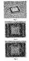
- FIGS. 2 to 5 show the results of the AC tests using the solder paste 1 to be used according to the invention, in which different thicknesses of the solder deposit were applied, as shown in Table 2.
- the results of the experiments in which the thickness of the solder deposit lies in a range between 100 and 160 ⁇ m, show very good to good test results
- Fig. 2 Measurement of solder paste 1 at 100 ⁇ m
- Fig. 3 Measurement of solder paste 1 at 120 ⁇ m
- Fig. 4 Measurement of solder paste 1 at 160 ⁇ m.
- the solder paste at a Lotdepotdicke of 160 microns FIG.
Landscapes
- Engineering & Computer Science (AREA)
- Mechanical Engineering (AREA)
- Manufacturing & Machinery (AREA)
- Microelectronics & Electronic Packaging (AREA)
- Electric Connection Of Electric Components To Printed Circuits (AREA)
Priority Applications (8)
| Application Number | Priority Date | Filing Date | Title |
|---|---|---|---|
| EP13197640.9A EP2886244A1 (fr) | 2013-12-17 | 2013-12-17 | Procédé de fixation d'un composant sur un substrat |
| KR1020167019334A KR20160102230A (ko) | 2013-12-17 | 2014-12-12 | 기판 위에 부품을 실장하기 위한 방법 |
| PCT/EP2014/077559 WO2015091260A1 (fr) | 2013-12-17 | 2014-12-12 | Procédé de fixation d'un composant sur un substrat |
| US15/105,378 US20160316572A1 (en) | 2013-12-17 | 2014-12-12 | Method for mounting a component on a substrate |
| SG11201604950QA SG11201604950QA (en) | 2013-12-17 | 2014-12-12 | Method for securing a component to a substrate |
| CN201480069205.3A CN105813798A (zh) | 2013-12-17 | 2014-12-12 | 在基底上固定部件的方法 |
| MX2016007749A MX2016007749A (es) | 2013-12-17 | 2014-12-12 | Metodo para asegurar un componente a un sustrato. |
| JP2016539139A JP2017507025A (ja) | 2013-12-17 | 2014-12-12 | 部品を基板に実装する方法 |
Applications Claiming Priority (1)
| Application Number | Priority Date | Filing Date | Title |
|---|---|---|---|
| EP13197640.9A EP2886244A1 (fr) | 2013-12-17 | 2013-12-17 | Procédé de fixation d'un composant sur un substrat |
Publications (1)
| Publication Number | Publication Date |
|---|---|
| EP2886244A1 true EP2886244A1 (fr) | 2015-06-24 |
Family
ID=49816849
Family Applications (1)
| Application Number | Title | Priority Date | Filing Date |
|---|---|---|---|
| EP13197640.9A Withdrawn EP2886244A1 (fr) | 2013-12-17 | 2013-12-17 | Procédé de fixation d'un composant sur un substrat |
Country Status (8)
| Country | Link |
|---|---|
| US (1) | US20160316572A1 (fr) |
| EP (1) | EP2886244A1 (fr) |
| JP (1) | JP2017507025A (fr) |
| KR (1) | KR20160102230A (fr) |
| CN (1) | CN105813798A (fr) |
| MX (1) | MX2016007749A (fr) |
| SG (1) | SG11201604950QA (fr) |
| WO (1) | WO2015091260A1 (fr) |
Families Citing this family (2)
| Publication number | Priority date | Publication date | Assignee | Title |
|---|---|---|---|---|
| JP6674982B2 (ja) * | 2017-08-30 | 2020-04-01 | 株式会社タムラ製作所 | はんだ組成物および電子基板 |
| US10913132B2 (en) | 2017-08-30 | 2021-02-09 | Tamura Corporation | Solder composition, electronic board, and bonding method |
Citations (7)
| Publication number | Priority date | Publication date | Assignee | Title |
|---|---|---|---|---|
| GB2198676A (en) * | 1986-12-03 | 1988-06-22 | Multicore Solders Ltd | Solder cream composition |
| DE19511392A1 (de) | 1994-03-31 | 1995-10-05 | Fraunhofer Ges Forschung | Verfahren und Vorrichtung zur Herstellung von Lothöckern |
| US5672542A (en) | 1994-08-08 | 1997-09-30 | Hewlett Packard Company | Method of making solder balls by contained paste deposition |
| WO2002020211A1 (fr) | 2000-09-07 | 2002-03-14 | Infineon Techonologies Ag | Brasure a utiliser dans des procedes de brasage par diffusion, et procede pour realiser des assemblages par brasage a l'aide de ladite brasure |
| US20030168123A1 (en) * | 2002-03-07 | 2003-09-11 | Kenichi Wada | Flux for solder paste and solder paste |
| DE102009034483A1 (de) * | 2009-07-22 | 2011-01-27 | W.C. Heraeus Gmbh | Bleifreie Hochtemperaturverbindung für die AVT in der Elektronik |
| US20130082094A1 (en) * | 2011-09-30 | 2013-04-04 | Rohm And Haas Electronic Materials Llc | Polyamine, carboxylic acid flux composition and method of soldering |
Family Cites Families (12)
| Publication number | Priority date | Publication date | Assignee | Title |
|---|---|---|---|---|
| AU5919890A (en) * | 1989-08-14 | 1991-02-14 | Multicore Solders Limited | Manufacture of printed circuit board assemblies |
| JP3273961B2 (ja) * | 1991-12-18 | 2002-04-15 | トヨタ自動車株式会社 | クリームはんだ |
| US5272007A (en) * | 1992-02-21 | 1993-12-21 | Union Carbide Chemicals & Plastics Technology Corporation | Solder powder coated with parylene |
| JP3311282B2 (ja) * | 1997-10-13 | 2002-08-05 | 株式会社東芝 | 金属部材の接合方法及び接合体 |
| US6217671B1 (en) * | 1999-12-14 | 2001-04-17 | International Business Machines Corporation | Composition for increasing activity of a no-clean flux |
| US6524398B2 (en) * | 2000-04-13 | 2003-02-25 | Fry's Metals, Inc. | Low-residue, low-solder-ball flux |
| DE102005053553A1 (de) * | 2005-11-08 | 2007-05-16 | Heraeus Gmbh W C | Lotpasten mit harzfreien Flussmittel |
| US7767032B2 (en) * | 2006-06-30 | 2010-08-03 | W.C. Heraeus Holding GmbH | No-clean low-residue solder paste for semiconductor device applications |
| JP2008062253A (ja) * | 2006-09-05 | 2008-03-21 | Denso Corp | はんだ付け用フラックスおよびはんだペースト組成物 |
| KR20140023266A (ko) * | 2010-12-17 | 2014-02-26 | 아라까와 가가꾸 고교 가부시끼가이샤 | 무연 땜납용 플럭스 및 무연 땜납 페이스트 |
| US8430294B2 (en) * | 2011-09-30 | 2013-04-30 | Rohm And Haas Electronic Materials Llc | Amine, carboxylic acid flux composition and method of soldering |
| US9950393B2 (en) * | 2011-12-23 | 2018-04-24 | Intel Corporation | Hybrid low metal loading flux |
-
2013
- 2013-12-17 EP EP13197640.9A patent/EP2886244A1/fr not_active Withdrawn
-
2014
- 2014-12-12 CN CN201480069205.3A patent/CN105813798A/zh active Pending
- 2014-12-12 SG SG11201604950QA patent/SG11201604950QA/en unknown
- 2014-12-12 KR KR1020167019334A patent/KR20160102230A/ko not_active Ceased
- 2014-12-12 JP JP2016539139A patent/JP2017507025A/ja active Pending
- 2014-12-12 MX MX2016007749A patent/MX2016007749A/es unknown
- 2014-12-12 US US15/105,378 patent/US20160316572A1/en not_active Abandoned
- 2014-12-12 WO PCT/EP2014/077559 patent/WO2015091260A1/fr not_active Ceased
Patent Citations (7)
| Publication number | Priority date | Publication date | Assignee | Title |
|---|---|---|---|---|
| GB2198676A (en) * | 1986-12-03 | 1988-06-22 | Multicore Solders Ltd | Solder cream composition |
| DE19511392A1 (de) | 1994-03-31 | 1995-10-05 | Fraunhofer Ges Forschung | Verfahren und Vorrichtung zur Herstellung von Lothöckern |
| US5672542A (en) | 1994-08-08 | 1997-09-30 | Hewlett Packard Company | Method of making solder balls by contained paste deposition |
| WO2002020211A1 (fr) | 2000-09-07 | 2002-03-14 | Infineon Techonologies Ag | Brasure a utiliser dans des procedes de brasage par diffusion, et procede pour realiser des assemblages par brasage a l'aide de ladite brasure |
| US20030168123A1 (en) * | 2002-03-07 | 2003-09-11 | Kenichi Wada | Flux for solder paste and solder paste |
| DE102009034483A1 (de) * | 2009-07-22 | 2011-01-27 | W.C. Heraeus Gmbh | Bleifreie Hochtemperaturverbindung für die AVT in der Elektronik |
| US20130082094A1 (en) * | 2011-09-30 | 2013-04-04 | Rohm And Haas Electronic Materials Llc | Polyamine, carboxylic acid flux composition and method of soldering |
Also Published As
| Publication number | Publication date |
|---|---|
| JP2017507025A (ja) | 2017-03-16 |
| KR20160102230A (ko) | 2016-08-29 |
| MX2016007749A (es) | 2016-12-12 |
| CN105813798A (zh) | 2016-07-27 |
| SG11201604950QA (en) | 2016-08-30 |
| WO2015091260A1 (fr) | 2015-06-25 |
| US20160316572A1 (en) | 2016-10-27 |
Similar Documents
| Publication | Publication Date | Title |
|---|---|---|
| EP3186032B1 (fr) | Procédé de production d'une liaison soudée | |
| EP2456589B1 (fr) | Connection sans plomb à haute temperature | |
| DE102012222791A1 (de) | Verfahren zur Kontaktierung eines Halbleiters und Halbleiterbauelement mit erhöhter Stabilität gegenüber thermomechanischen Einflüssen | |
| DE102015107724B4 (de) | Verfahren zum Herstellen einer Substratanordnung, Substratanordnung, Verfahren zum Verbinden eines Elektronikbauteils mit einer Substratanordnung und Elektronikbauteil | |
| DE102013107065A1 (de) | Bolzenkontakthügelstruktur und Verfahren zum Herstellen derselben | |
| EP2572814A1 (fr) | Pâte et procédé de connexion d'un composant électronique doté d'un substrat | |
| DE102021124877A1 (de) | Lotmaterial, schichtstruktur, chipgehäuse, verfahren zum herstellen einer schichtstruktur und verfahren zum herstellen eines chipgehäuses | |
| EP2886245B1 (fr) | Pâte de brasage avec acide adipique, acide oxalique et composants aminés | |
| EP2942129B1 (fr) | Pâte métallique et son utilisation pour relier des éléments de construction | |
| DE102014105957B3 (de) | Verfahren zur Herstellung einer Lötverbindung | |
| EP3186033B1 (fr) | Pâte à braser et procédé de connection cohésive | |
| EP2886244A1 (fr) | Procédé de fixation d'un composant sur un substrat | |
| EP2957366B1 (fr) | Pâte métallique et son utilisation pour relier des éléments de construction | |
| DE102019126505B4 (de) | Verfahren zum herstellen einer mehrchipvorrichtung | |
| DE102017122059A1 (de) | Verfahren zur Herstellung einer Endoberfläche und Leiterplatte | |
| EP4086031A1 (fr) | Alliage | |
| DE102019009176A1 (de) | Verfahren zum bilden einer metallzwischenverbindung | |
| DE102019129971A1 (de) | Verfahren zum Auflöten eines Bauelements auf eine Leiterplatte, Elektronikeinheit und Feldgerät der Automatisierungstechnik | |
| DE102010041917B4 (de) | Schaltungsanordnung und Verfahren zu deren Herstellung | |
| DE102023201060A1 (de) | Verfahren sowie Fertigungsvorrichtung zur Herstellung einer stoffschlüssigen, elektrisch leitfähigen Schnittstelle für eine Verbindung von elektronischen Bauteilen | |
| DE102011083911A1 (de) | Elektronische Baugruppe mit hochtemperaturstabilem Substratgrundwerkstoff | |
| EP3782764A1 (fr) | Combinaison de pâte de cuivre / métal d'apport de brasage destinée à la production de composés de soudure sans plomb stables à température élevée | |
| DE2042370B2 (de) | Lottrager und denselben enthal tende Lotpaste | |
| DE102021207267A1 (de) | Als temporäres Fixiermittel verwendbare Zusammensetzung | |
| DE102014111435B4 (de) | Chip-Anordnung |
Legal Events
| Date | Code | Title | Description |
|---|---|---|---|
| PUAI | Public reference made under article 153(3) epc to a published international application that has entered the european phase |
Free format text: ORIGINAL CODE: 0009012 |
|
| 17P | Request for examination filed |
Effective date: 20131217 |
|
| AK | Designated contracting states |
Kind code of ref document: A1 Designated state(s): AL AT BE BG CH CY CZ DE DK EE ES FI FR GB GR HR HU IE IS IT LI LT LU LV MC MK MT NL NO PL PT RO RS SE SI SK SM TR |
|
| AX | Request for extension of the european patent |
Extension state: BA ME |
|
| STAA | Information on the status of an ep patent application or granted ep patent |
Free format text: STATUS: REQUEST FOR EXAMINATION WAS MADE |
|
| STAA | Information on the status of an ep patent application or granted ep patent |
Free format text: STATUS: THE APPLICATION IS DEEMED TO BE WITHDRAWN |
|
| 18D | Application deemed to be withdrawn |
Effective date: 20180703 |