EP2887355A1 - Cellule de stockage de données et agencement de mémoire - Google Patents
Cellule de stockage de données et agencement de mémoire Download PDFInfo
- Publication number
- EP2887355A1 EP2887355A1 EP13198871.9A EP13198871A EP2887355A1 EP 2887355 A1 EP2887355 A1 EP 2887355A1 EP 13198871 A EP13198871 A EP 13198871A EP 2887355 A1 EP2887355 A1 EP 2887355A1
- Authority
- EP
- European Patent Office
- Prior art keywords
- data storage
- storage cell
- data
- control gate
- output node
- Prior art date
- Legal status (The legal status is an assumption and is not a legal conclusion. Google has not performed a legal analysis and makes no representation as to the accuracy of the status listed.)
- Withdrawn
Links
- 210000000352 storage cell Anatomy 0.000 title claims abstract description 85
- 238000013500 data storage Methods 0.000 title claims abstract description 83
- 230000015654 memory Effects 0.000 title claims abstract description 77
- 230000000295 complement effect Effects 0.000 claims abstract description 47
- 238000000034 method Methods 0.000 claims abstract description 28
- 238000007667 floating Methods 0.000 claims description 5
- 210000004027 cell Anatomy 0.000 description 100
- 230000005669 field effect Effects 0.000 description 11
- 238000005265 energy consumption Methods 0.000 description 5
- 230000003068 static effect Effects 0.000 description 5
- 230000001419 dependent effect Effects 0.000 description 4
- 230000008520 organization Effects 0.000 description 4
- 238000005516 engineering process Methods 0.000 description 2
- 229910044991 metal oxide Inorganic materials 0.000 description 2
- 150000004706 metal oxides Chemical class 0.000 description 2
- 230000009467 reduction Effects 0.000 description 2
- 230000002040 relaxant effect Effects 0.000 description 2
- 239000004065 semiconductor Substances 0.000 description 2
- 241001481828 Glyptocephalus cynoglossus Species 0.000 description 1
- 101000985296 Homo sapiens Neuron-specific calcium-binding protein hippocalcin Proteins 0.000 description 1
- 101000935117 Homo sapiens Voltage-dependent P/Q-type calcium channel subunit alpha-1A Proteins 0.000 description 1
- 241000665848 Isca Species 0.000 description 1
- 102100025330 Voltage-dependent P/Q-type calcium channel subunit alpha-1A Human genes 0.000 description 1
- 238000010420 art technique Methods 0.000 description 1
- 238000007599 discharging Methods 0.000 description 1
- 238000005065 mining Methods 0.000 description 1
- 230000007935 neutral effect Effects 0.000 description 1
- 239000000758 substrate Substances 0.000 description 1
Images







Classifications
-
- G—PHYSICS
- G11—INFORMATION STORAGE
- G11C—STATIC STORES
- G11C23/00—Digital stores characterised by movement of mechanical parts to effect storage, e.g. using balls; Storage elements therefor
-
- G—PHYSICS
- G11—INFORMATION STORAGE
- G11C—STATIC STORES
- G11C11/00—Digital stores characterised by the use of particular electric or magnetic storage elements; Storage elements therefor
- G11C11/54—Digital stores characterised by the use of particular electric or magnetic storage elements; Storage elements therefor using elements simulating biological cells, e.g. neuron
-
- H—ELECTRICITY
- H01—ELECTRIC ELEMENTS
- H01H—ELECTRIC SWITCHES; RELAYS; SELECTORS; EMERGENCY PROTECTIVE DEVICES
- H01H1/00—Contacts
- H01H1/0094—Switches making use of nanoelectromechanical systems [NEMS]
Definitions
- the invention relates to the field of memory cells and memory arrangements. More particularly, the present invention relates to non-volatile memory cells and memory arrangements thereof based on nano electromechanical switches.
- SRAM memory cells suffer from a number of issues : they are energy-inefficient, both from a dynamic energy consumption perspective and from a leakage energy perspective. Even if standby leakage can be mitigated by recent state-of-the-art techniques, active leakage due to SRAM remains an issue. Furthermore, for both read and write operations, data typically is to be provided at a speed depending on the location of the memory in the memory hierarchy. For example, in L3 cache, up to 10 cycles may be used. For SRAM memory cells, typically a trade-off is made between speed, area and energy consumption. SRAM memory cells also are volatile, meaning that they lose their data when in a power-off state. Furthermore, SRAM memory cells typically use up large areas of the substrate, amongst others because they require large area per bit. An area reduction would be welcome.
- solutions based on emerging non-volatile memories such as STT-MRAM and RRAM.
- compact non-volatile memory cells as now known have a read current flowing through the memory element so that no high performance read is possible.
- the current must be low enough to avoid cell state disturbance.
- the resistance level of the memory element must be selected in such a way that both read and write operations can be accommodated, which limit the options to improve read performance. Cells that avoid this current through the memory element typically are much less compact and often are not robust to transistor variations.
- the energy consumption of the memory cell can be substantially lower than for SRAM memory cells.
- the present invention relates to a data storage cell for storing data, the data storage cell comprising
- the nano electromechanical switches are vertical nano electromechanical switches, wherein the beam is oriented substantially vertically with respect to the average plane through both control gates of the NEM switch. It is an advantage of embodiments of the present invention that a data storage cell with a small memory footprint can be obtained.
- the data storage cell furthermore may comprise at least a first read selector, comprising a first, second and third selector terminal, the first selector terminal being connected to the first output node (Q), the second selector terminal being connected to a read bit line (RBL) and the third selector terminal being connected to a DC bias or a second data line (RVSS). It is an advantage of embodiments according to the present invention that a data storage cell with fast read-out capabilities can be obtained.
- the first read selector may be a field-effect transistor element. It may be an NMOS element. It is an advantage of embodiments of the present invention that read current can be routed through a single FET.
- the first and/or the second read selector may be a MOSFET.
- the first and second nano electromechanical switch may comprise a common second node or each may comprise a separate second node against which their moveable beam can be positioned.
- the second node may be a floating node or may be a second output node.
- the data storage cell may comprise two read selectors, the first read selector being connected to the first output node and the second read selector being connected to the second output node, the second read selector thus providing the complementary read from the first read selector. It is an advantage of embodiments according to the present invention that it is easy to enhance read performance by providing a complementary read selector and read bit line.
- the second read selector also may be a field-effect transistor element. It may be an NMOS element. It is an advantage of embodiments of the present invention that read current can be routed through a single FET.
- the second read selector may be a MOSFET.
- the first and the second anchor may be connected to data lines for providing data to be stored to the data storage cell and wherein the first and second control gate, respectively the third and the fourth control gate are connected with write word lines and configured for enabling the movement of the first moveable beam respectively the second moveable beam according to the data provided to the anchors.
- the first respectively the second anchor may be connected with word lines (WL, WLG) for enabling the movement of the first moveable beam respectively the second moveable beam and the first and second control gate, respectively the third and the fourth control gate may be connected with data lines for providing data to be stored to the data storage cell.
- word lines WL, WLG
- the present invention also relates to a memory arrangement that may comprise a plurality of data storage cells, one or more of the data storage cells being a data storage cell as described above.
- the present invention also relates to a method for writing data to a data storage cell comprising two nano electromechanical (NEM) switches, the two nano electromechanical (NEM) switches comprising respectively a first anchor, first control gate, second control gate and a second anchor, third control gate and fourth control gate, the method comprising controlling moveable beams of the first, respectively the second NEM switch so that one of the moveable beams contacts a first output node of the data storage cell, whereas the other moveable beam contacts another node of the data storage cell, and writing data to the data storage cell by providing an electrical signal to the first and second anchors and to the first, second, third and fourth control gates.
- NEM nano electromechanical
- Said controlling and writing may comprise providing a first digital state at a write control gate of the first NEM switch and a complementary /write control gate of the second NEM switch and providing a second digital state, complementary to the first digital state, at a write control gate of the second NEM switch and a complementary /write control gate of the first NEM switch, thus controlling positioning of the moveable beams and providing data to be stored.
- the electrical signals applied to the control gates may enable the movement of the beams, and the electrical signals applied to the anchors may determine the data that is to be written.
- the electrical signals applied to the anchors may enable the movement of the beams, and the electrical signals applied to the control gates may determine the data that is written.
- embodiments of the present invention relate to a data storage cell for storing data.
- the data storage cell can advantageously be used as an SRAM replacement circuit component for use in embodiments of the present invention, e.g. a basic element in an embedded memory system, such as a cache memory, a GPU memory or scratchpad memory.
- SRAM replacement circuit component for use in embodiments of the present invention, e.g. a basic element in an embedded memory system, such as a cache memory, a GPU memory or scratchpad memory.
- the NEM switches can for example be implemented as a vertical switch, furthermore resulting in data storage cells with low footprint, which can result in dense memory arrangements.
- the data storage cell comprises a first and a second nano electromechanical switch.
- the first nano electromechanical switch comprises a first moveable beam fixed to a first anchor, a first control gate and a second control gate, a first output node against which the first moveable beam can be positioned.
- the second nano electromechanical switch comprises a second moveable beam fixed to a second anchor, a third control gate and a fourth control gate, the second moveable beam also can be positioned against the first output node.
- the first nano electromechanical switch and the second nano electromechanical switch are configured for actuating a first or a second state of the data storage cell. Furthermore they are configured for having their moveable beam complementary positioned to the first output node. With complementary positioned, reference is made to the situation wherein the second moveable beam is not positioned against the first output node when the first moveable beam is positioned against the first output node. It is an advantage of embodiments of the present invention that a non-volatile and low-power memory architecture can be provided.
- the data storage cell furthermore comprises at least a first read selector comprising a first, second and third terminal. The first selector terminal thereby is connected to the first output node (Q).
- the output node thereby is an inner of the NEM switches part.
- the second selector terminal typically is connected to a read bit line (RBL).
- the third selector terminal typically is being connected to a DC bias or a second data line (RVSS).
- the read selector may in some examples be a field-effect transistor element, for example be a MOSFET, although embodiments are not limited thereto.
- the NEM switches also comprise a second node configured as second output node for outputting the complementary read out and the cell comprises a second read selector connected with the second output node.
- the data storage cell may be adapted for different read out or write schemes.
- first and the second anchor are connected to data lines for providing data to be stored to the data storage cell and the control gates are connected with write word lines and configured for controlling the movement of the moveable beams.
- first and second anchor are connected to write word lines for controlling the movement of the moveable beams and the control gates are connected to data lines for providing data to be stored to the data storage cell.
- the present invention also relates to a non-volatile memory arrangement.
- a memory arrangement comprises a plurality of data storage cells where advantageously all, but at least one or more of the data storage cells are data storage cells according to an embodiment as described in the first aspect.
- the memory arrangement comprises a plurality of data storage cells arranged in an array, whereby the data storage cells are provided as translated identical copies, advantageously reducing cross-talk between read bit lines of adjacent cells, as will be further illustrates in the examples.
- the read bit line and the supply line may be twisted to cancel disturbance on neighbouring lines.
- Other particular arrangements may be provided, taking into arrangement rules as known by the person skilled in the art.
- embodiments of the current invention relate to the use of the data storage cells in a memory arrangement for storing data or for controlling the operation of circuits.
- a memory arrangement may be used in a variety of applications, such as for example applications making use of configurable routing or configurable logic, or as content-addressable memory.
- embodiments of the present invention relate to methods for writing and reading data storage cells.
- a method for writing data to a data storage cell comprising two nano electromechanical (NEM) switches.
- Such a method comprises controlling moveable beams of the first, respectively the second NEM switch so that one of the moveable beams contacts a first output node of the data storage cell, whereas the other moveable beam contacts another node of the data storage cell.
- the method also comprises writing data to the data storage cell by providing an electrical signal to the first and second anchors and to the first, second, third and fourth control gates. Particular writing schemes will be discussed in more detail in the examples discussed below.
- the electrical signals applied to the control gates enable the movement of the beams and the electrical signals applied to the anchors determines the data that is written.
- the data to be written thus is provided via two data lines that contact the anchor of the first respectively the second NEM switch of the cell.
- the beams are hence sensitized for writing by the write and /write control lines, and the state to be written is controlled by the data lines.
- the electrical signals applied to the anchors enable the movement of the beams, and the electrical signals applied to the control gates determine the data that is written.
- the writing process comprises providing control data for controlling the movement of the moveable beams via an anchor of the moveable beams and providing data-dependent control signals via control gates of the EM switches for providing data to be stored to the data storage cell.
- the method comprises reading of data storage cells.
- the method may typically comprise controlling moveable beams of the first, respectively the second NEM switch so that one of the moveable beams contacts a first output node of the data storage cell, whereas the other moveable beam contacts another node of the data storage cell, and providing electrical control signals for controlling at least one read selector so as to read out a signal from the first output node of the data storage cell.
- the read selector may be a FET, e.g. a MOSFET.
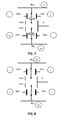
- FIG. 1 and FIG. 2 schematically show a first exemplary data storage cell.
- This circuit comprises a pair of nano electromechanical (NEM) switches.
- the pair of NEM switches can be actuated to switch the circuit in either one of two states, cell state 0 and cell state 1, respectively illustrated in FIG. 1 and FIG. 2 .
- the data bit state is stored in two complementary NEM switches, e.g. the first NEM switch 102 and the second NEM switch 103.
- the first NEM switch 102 comprises a movable beam 101 which can be actuated by applying a write signal write and its complement /write to respectively a first and second control gate.
- an electrical signal w A which is provided via a first anchor/source terminal can be electrically connected to or disconnected from the first output node Q.
- the second NEM switch 103 also comprises a movable beam 104 which can be actuated by applying a write signal /write and its complement write to respectively a first and a second control gate.
- an electrical signal w B which is provided via a second anchor/source terminal can be electrically connected to or disconnected from the first output node Q.
- the two NEM switches 102,103 are complementary in the sense that when the movable beam 101 enables the electrical signal wA to flow to the first output node Q, the second movable beam 104 disables conduction of the electrical signal wB to the first output node Q, and vice versa.
- the output node Q is either connected to W A or to W B .
- the beam 101,104 When the movable beam 101,104 is not connected to the output node Q, the beam 101,104 may be connected to an electrically floating node.
- This floating node may be a separate node for movable beam 101 and movable beam 104, e.g. electrically isolated from each other, as shown in FIG. 1 and FIG. 2 , or may be a merged node for movable beam 101 and movable beam 104.
- the movable beam 101,104 when not connected to the output node Q, the movable beam 101,104 may also be connected to a second output node Q bar , which thus provides a complementary output.
- FIG. 3 to FIG. 5 A first method for writing data to the storage cell with two complementary NEM switches illustrated in FIG. 1 and FIG. 2 is illustrated in FIG. 3 to FIG. 5 .
- This first method corresponds to a straightforward biasing scheme, in which the data to be stored is provided via the electrical signals W A and W B , while the write signal write and its complement /write are used to sensitize the beams, e.g. to impose a write event of the supplied data.
- FIG. 3 illustrates operation of the circuit in accordance with this first method for a write event of a digital 0 state.
- a signal representing the digital 0 state e.g. a low or zero voltage state
- a digital 1 state e.g. a high voltage state
- a complementary digital 0 state is provided at the /write control gates.
- FIG. 4 illustrates operation for a write event of a digital 1 state.
- the electrical signals w A and w B are supplied such as to correspond to a digital 0 state.
- FIG. 5 illustrates that cells that are connected to actuated w A and w B lines, but not to activated write lines (half-selected cells) do not suffer state loss. For non-activate write lines, write and /write are put at the same potential, e.g. 0. Half-selected cells do not suffer state loss, as for each beam, the electrostatic actuation force of the two control gates substantially cancel one another.
- FIG. 6 to FIG. 8 A second method for writing data to the storage cell with two complementary NEM switches illustrated in FIG. 1 and FIG. 2 is illustrated in FIG. 6 to FIG. 8 .
- the data to be stored and its complement are respectively provided via the write signals write and /write, and the electrical signals W A and W B are used to sensitize the beams for a write event.
- this method might be more complex than the first method, it may advantageously integrate well into a memory array architecture, e.g. can handle bit line and word line addressing efficiently.
- FIG. 6 illustrates operation of the circuit in accordance with this second method for a write event of a digital 0 state.
- a signal representing a positive state + e.g. a positive voltage state
- the complementary negative state - e.g. a negative voltage state
- the electrical signals WL A and WL B are also supplied as a positive + state to sensitize the beams for writing.
- the cell switches to the 0 state in which the WL A line connects to the first output node Q.
- FIG. 7 illustrates a write event of a digital 1 state.
- a signal corresponding to a negative state - is supplied via the write control gates, and the complementary positive state + is supplied via the /write gates.
- the electrical signals WL A and WL B correspond to a positive + state to initiate a write event.
- the cell switches to the 1 state in which the WL B line connects to the first output node Q.
- FIG. 8 illustrates the situation whereby disturbance of write data line half-selected cells is avoided.
- Cells in non-selected words are exposed to the same WDL and /WDL as the cells in the word that is to be written.
- WL A and WL B equal to 0, no net electrostatic force is felt by the beams.
- FIG. 9 illustrates the situation whereby disturbance of word line half selected cells is avoided.
- the electrical signal WL A may correspond to a state A, e.g. either - or +, while the electrical signal WL B corresponds to a state B, e.g. either - or +, e.g. equal or complementary to A.
- a neutral signal is provided to both the write and the /write control gates, e.g. a ground voltage state, such as the mean of the positive state + and negative state - potentials.
- the cell maintains its current state, and depending on this current state, the signal WL A or WL B is supplied to the first output node Q.
- FIG. 10 and FIG. 11 schematically show a device comprising such a data storage cell, e.g. an SRAM replacement circuit component, for use in embodiments of the present invention.
- This circuit comprises a pair of nano electromechanical (NEM) switches and a field-effect transistor element, e.g. a metal-oxide semiconductor field-effect transistor (MOSFET).
- NEM nano electromechanical
- MOSFET metal-oxide semiconductor field-effect transistor
- the data storage cell comprises a pair of NEM switches which can be actuated to switch the circuit in either one of two states, cell state 0 and cell state 1, respectively illustrated in FIG. 10 and FIG. 11 .
- the first output node Q is connected to a gate terminal of the field-effect transistor element 107, e.g. a NMOS element.
- This transistor 107 connects a read-bitline RBL to a voltage supply line RVSS, e.g. whereby in one example RVSS may be 0V, but other voltages also can be selected.
- RVSS voltage supply line
- the read current may pass through a single transistor element, which may provide an advantageously fast bitline discharge compared to other single-ended cells.
- the bit line precharge level may be freely selected, unlike in the case of traditional 6T SRAM cells, where a low BL precharge voltage ( ⁇ Vdd - V threshold, NMOS ) results in read disturbs. Furthermore, a low energy consumption compared to SRAM may be achieved.
- the first anchor terminal and the second anchor terminal may be respectively connected to a first word line WL and a second word line WLG, while a write data line WDL is connected to respectively the first control gate of the first NEM switch 102 and the second control gate of the second NEM switch 103, and a complementary write digit line /WDL to respectively the second control gate of the first NEM switch 102 and the first control gate of the second NEM switch 103.
- a corresponding array organization scheme for this second data storage cell is schematically shown in FIG. 12 .
- FIG. 13 and FIG. 14 An exemplary readout of the device is illustrated in FIG. 13 and FIG. 14 , for respectively a cell in state 0 and a cell in state 1.
- the cell data content is stored in the complementary NEM switches 102 and 103.
- all non-active word lines WL and WLG may set to the digital 0 level.
- the read bit line RBL may be precharged to a certain voltage V prech , e.g. a positive supply voltage Vdd or 0.2V, and the selected word line WL, e.g. the active word line, is set to the digital 1 level.
- V prech e.g. a positive supply voltage Vdd or 0.2V
- the selected word line WL e.g. the active word line
- the read bit line RBL is discharged or not, e.g.
- the stored value supplied over the read bit line RBL may be read as in a conventional SRAM, e.g. with a sense amplifier.
- a memory chip may be manufactured which is smaller than 6T SRAM, for example comparable to RRAM/STT-MRAM.
- leakage may be advantageously low or even substantially zero.
- the read current can be routed through a single field-effect transistor instead of two FETs in series.
- a fast bit line discharge can be achieved, e.g. twice as fast as in conventional SRAM technology.
- the disclosed memory cell according to embodiments furthermore may not require a static write current.
- the memory cell is furthermore adaptable in terms of a freely selectable bit line precharge voltage, e.g. a low V prech can be selected to achieve a low energy consumption.
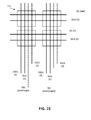
- FIG. 15 shows a read biasing scheme in accordance with embodiments of the present invention.
- the write digital lines WDL and /WDL are set to digital 0 for all cells in the array.
- the first word line WL is set to digital 1
- the second word line WLG is set to digital 0.
- the precharged bit line BL is discharged by a bit line current I BL .
- the first word line WL and the second word line WLG are both set to digital 0. If the cell is in state 0, the first output node Q is connected to the first word line WL, and if the cell is in state 1, the first output node Q is connected to the second word line WLG. In either case, the first output node Q is set to digital 0. Therefore, no discharge current I BL flows through the FET element, e.g. the bit line BL is in the bit line half selected cells isolated via a high impedance path through the FET.
- word line WL connects the cells of more than one word
- word line half selected (WLHS) cells For these cells, the first word line WL is set to digital 1, while the second word line WLG is set to digital 0, as for the selected cell. If the cell is in state 0, the first output node Q is connected to the first word line WL, and thus also set to the digital 1 state. Therefore, the bit line BL would be discharged if it were precharged, which consumes energy.
- An advantage compared to conventional 6T SRAM is that it is possible to not precharge BLs that do not contain selected cells without risking cell state disturbance.
- FIG. 16 shows a write biasing scheme in accordance with embodiments of the present invention.
- This write biasing scheme may be atypical compared to regular cell configurations because the anchor lines must be parallel to the first word line WL.
- the non-selected word lines WL and WLG may be biased at equal distance from the actuation values used for the write digital line WDL and its complement /WDL. Nevertheless, some deviation from this rule can be accommodated if the NEM switch has sufficient hysteresis to keep its state even if it experiences some partial net write voltage.
- the first word line WL and the second word line WLG should be at substantially equal potential to avoid static current through cell
- the write digital line WDL is set to the positive + state and the complementary write digital line /WDL is set to the negative - state, e.g. to equal but opposite voltages V w .
- the write digital line WDL is set to the negative - state and the complementary write digital line /WDL is set to the positive + state.
- both the first word line WL and the second word line WLG are set to digital 1.
- the top beam e.g. the beam of the first NEM switch experiences a potential 2V such that it is moved toward the first output node Q, e.g.
- the bottom beam e.g. the beam of the second NEM switch experiences a potential 2V in the opposite direction relative to the first NEM switch such that it is moved away from the first output node Q, e.g. such that the second word line WLG disconnects from the first output node Q.
- the top beam experiences a potential 2V such that it is moved away from the first output node Q such that the first word line WL disconnects from the first output node Q.
- the bottom beam experiences a potential 2V in the opposite direction relative to the first NEM switch such that it is moved toward the first output node Q, e.g. such that the second word line WLG connects to the first output node Q.
- the first word line WL and the second word line WLG are both set to digital 0.
- the write digital line WDL and the complementary write digital line /WDL are both set to opposite states, as for the active cell.
- both the top beam and the bottom beam experience a net force which is substantially zero.
- the beams are attracted with equal force to both control gates and hence the forces cancel out, i.e. balance one another.
- the latter can be understood as follows. Taking a voltage V1 at control gate 1 and V2 at control gate 2, the beam is at (V1+V2)/2, assuming first order formulas.
- V ⁇ 1 - V ⁇ 2 + V ⁇ 1 / 2 2 C . V ⁇ 1 - V ⁇ 2 / 2 2
- these forces are equal, they indeed cancel one another.
- the top beam experiences opposing and substantially equal forces towards its two control gates, resulting in a substantially zero net force.
- the WLHS cells experience the following bias condition.
- the first word line WL and the second word line WLG are set to 1V.
- WDL and /WDL are set to the same voltage, e.g. 0V.
- Both the top beam and the bottom beam experience a potential 1V-x toward the output node and a potential 1V-x away from the output node, such that again no net force is exerted on either beam.
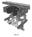
- FIG. 17 shows an exemplary layout of a memory cell according to embodiments of the present invention.
- the cells may be provided in a vertical arrangement, e.g. to facilitate implementation of the cells in an array, e.g. a rectangular grid when viewed along a direction parallel to the vertical. For simplicity, only two cells are shown.
- the cells may also be provided as translated identical copies in a memory layout.
- the latter may for example have the advantage of reduced crosstalk between the read bit lines RBL of adjacent cells.
- the RVSS line may also be used as an additional signal line.
- the read bit line RBL and the supply RVSS may also be twisted to cancel out crosstalk between neighboring lines.
- FIG. 18 and FIG. 19 schematically show another example of a device comprising a data storage cell, e.g. an SRAM replacement circuit component, for use in embodiments of the present invention.
- This circuit comprises a pair of nano electromechanical (NEM) switches and pair of field-effect transistor elements, e.g. a metal-oxide semiconductor field-effect transistor (MOSFET).
- NEM nano electromechanical
- MOSFET metal-oxide semiconductor field-effect transistor
- the first output node Q is connected to a gate terminal of the first field-effect transistor element 107, e.g. a NMOS element.
- This transistor 107 connects a read-bitline RBL to a voltage supply line RVSS, whereby in one example RVSS may be 0V, but other voltages also can be selected.
- the movable beam 101, 104 when not connected to the output node Q, the movable beam 101, 104 is not switched to a floating state, but instead connects to a second output node /Q, and thus provides a complementary output, e.g. an output /Q which is complementary to the first output node Q.
- the second output node /Q is connected to a gate terminal of the second field-effect transistor element 112, e.g. a NMOS element.
- This transistor 112 connects a complementary read-bitline /RBL to the voltage supply line RVSS.
- the first anchor/source terminal and the second anchor/source terminal may be respectively connected to a first word line WL and a second word line WLG, while a write digit line WDL is connected to respectively the first control gate of the first NEM switch 102 and the second control gate of the second NEM switch 103, and a complementary write digit line /WDL to respectively the second control gate of the first NEM switch 102 and the first control gate of the second NEM switch 103.
- a complementary readout as provided by this third data storage cell according to embodiments of the present invention advantageously offers a redundant, complementary copy of the readout signal. Furthermore, the need for a separate reference voltage can be avoided, as the voltage on the read bit line RBL and the complementary read bit line /RBL can be directly compared to determine the output bit state.
- FIG. 20 shows an exemplary layout for a memory array comprising this third memory cell according to embodiments of the present invention.
- the cells may be provided in a vertical arrangement, e.g. to facilitate implementation of the cells in an array, e.g. a rectangular grid when viewed along a direction parallel to the vertical. For simplicity, only two cells are shown.
Landscapes
- Engineering & Computer Science (AREA)
- Health & Medical Sciences (AREA)
- Life Sciences & Earth Sciences (AREA)
- Biomedical Technology (AREA)
- General Health & Medical Sciences (AREA)
- Molecular Biology (AREA)
- Neurology (AREA)
- Computer Hardware Design (AREA)
- Semiconductor Memories (AREA)
Priority Applications (3)
| Application Number | Priority Date | Filing Date | Title |
|---|---|---|---|
| EP13198871.9A EP2887355A1 (fr) | 2013-12-20 | 2013-12-20 | Cellule de stockage de données et agencement de mémoire |
| JP2014233717A JP2015164086A (ja) | 2013-12-20 | 2014-11-18 | データストレージセル及びメモリ構成 |
| US14/558,505 US9911504B2 (en) | 2013-12-20 | 2014-12-02 | Non-volatile memory array using electromechanical switches for cell storage |
Applications Claiming Priority (1)
| Application Number | Priority Date | Filing Date | Title |
|---|---|---|---|
| EP13198871.9A EP2887355A1 (fr) | 2013-12-20 | 2013-12-20 | Cellule de stockage de données et agencement de mémoire |
Publications (1)
| Publication Number | Publication Date |
|---|---|
| EP2887355A1 true EP2887355A1 (fr) | 2015-06-24 |
Family
ID=49916879
Family Applications (1)
| Application Number | Title | Priority Date | Filing Date |
|---|---|---|---|
| EP13198871.9A Withdrawn EP2887355A1 (fr) | 2013-12-20 | 2013-12-20 | Cellule de stockage de données et agencement de mémoire |
Country Status (3)
| Country | Link |
|---|---|
| US (1) | US9911504B2 (fr) |
| EP (1) | EP2887355A1 (fr) |
| JP (1) | JP2015164086A (fr) |
Citations (4)
| Publication number | Priority date | Publication date | Assignee | Title |
|---|---|---|---|---|
| US20040175856A1 (en) * | 2001-07-25 | 2004-09-09 | Nantero, Inc. | Devices having vertically-disposed nanofabric articles and methods of marking the same |
| WO2008032069A1 (fr) * | 2006-09-13 | 2008-03-20 | Cavendish Kinetics Limited | Cellule binaire de mémoire non volatile |
| WO2009101516A1 (fr) * | 2008-02-14 | 2009-08-20 | Cavendish Kinetics, Ltd. | Cellule binaire à mémoire programmable, à temps multiple et trois bornes et architecture matricielle |
| US7719318B1 (en) * | 2008-11-05 | 2010-05-18 | Sandia Corporation | Nanoeletromechanical switch and logic circuits formed therefrom |
Family Cites Families (6)
| Publication number | Priority date | Publication date | Assignee | Title |
|---|---|---|---|---|
| WO2004088719A2 (fr) * | 2003-03-28 | 2004-10-14 | Nantero, Inc. | Nanotube sur structures tec de grille et applications correspondantes |
| CA2535634A1 (fr) * | 2003-08-13 | 2005-05-26 | Nantero, Inc | Elements de commutation a base de nanotubes comprenant des commandes multiples et circuits produits a partir de ces elements |
| US7583526B2 (en) * | 2003-08-13 | 2009-09-01 | Nantero, Inc. | Random access memory including nanotube switching elements |
| US7885103B2 (en) * | 2005-11-22 | 2011-02-08 | Agate Logic, Inc. | Non-volatile electromechanical configuration bit array |
| US20090273971A1 (en) * | 2008-04-30 | 2009-11-05 | Cavendish Kinetics Inc. | Continuously driving non-volatile memory element |
| US9460777B2 (en) * | 2013-08-02 | 2016-10-04 | Qualcomm Incorporated | SRAM read buffer with reduced sensing delay and improved sensing margin |
-
2013
- 2013-12-20 EP EP13198871.9A patent/EP2887355A1/fr not_active Withdrawn
-
2014
- 2014-11-18 JP JP2014233717A patent/JP2015164086A/ja active Pending
- 2014-12-02 US US14/558,505 patent/US9911504B2/en active Active
Patent Citations (4)
| Publication number | Priority date | Publication date | Assignee | Title |
|---|---|---|---|---|
| US20040175856A1 (en) * | 2001-07-25 | 2004-09-09 | Nantero, Inc. | Devices having vertically-disposed nanofabric articles and methods of marking the same |
| WO2008032069A1 (fr) * | 2006-09-13 | 2008-03-20 | Cavendish Kinetics Limited | Cellule binaire de mémoire non volatile |
| WO2009101516A1 (fr) * | 2008-02-14 | 2009-08-20 | Cavendish Kinetics, Ltd. | Cellule binaire à mémoire programmable, à temps multiple et trois bornes et architecture matricielle |
| US7719318B1 (en) * | 2008-11-05 | 2010-05-18 | Sandia Corporation | Nanoeletromechanical switch and logic circuits formed therefrom |
Non-Patent Citations (4)
| Title |
|---|
| "Energy Efficient Many-core Processor for Recognition and Mining using Spin-based Memory", IEEE LNT'L SYMP. ON NANOSCALE ARCHITECTURES, pages 122 - 128 |
| R.VENKATESAN ET AL.: "Spin Transfer Torque Magnetic RAM (STT-MRAM", RELAXING NON-VOLATILITY FOR FAST AND ENERGY-EFFICIENT STT-RAM CACHE |
| SMULLEN ET AL., IEEE INT'I SYMP. ON HPCA, February 2011 (2011-02-01), pages 50 - 61 |
| XIAOCHEN GUO ET AL.: "Resistive Computation: Avoiding the Power Wall with Low-Leakage, STT- MRAM Based Computing", ISCA, 2010, pages 371 - 382 |
Also Published As
| Publication number | Publication date |
|---|---|
| JP2015164086A (ja) | 2015-09-10 |
| US9911504B2 (en) | 2018-03-06 |
| US20150179278A1 (en) | 2015-06-25 |
Similar Documents
| Publication | Publication Date | Title |
|---|---|---|
| US8144509B2 (en) | Write operation for spin transfer torque magnetoresistive random access memory with reduced bit cell size | |
| US7596014B2 (en) | Semiconductor device | |
| CN103594111B (zh) | 包括多个静态随机访问存储器单元的装置及其操作方法 | |
| KR100673901B1 (ko) | 저전압용 반도체 메모리 장치 | |
| US9171618B2 (en) | Semiconductor integrated circuit and processor | |
| EP3096325B1 (fr) | Circuits à mémoire à accès aléatoire statique | |
| JP6421399B2 (ja) | Stt−mramを使用した半導体記憶装置 | |
| US20090103354A1 (en) | Ground Level Precharge Bit Line Scheme for Read Operation in Spin Transfer Torque Magnetoresistive Random Access Memory | |
| KR20050086362A (ko) | 반도체 집적회로 | |
| CN103123803A (zh) | 半导体存储装置 | |
| JP2007042172A (ja) | 半導体メモリ装置 | |
| Premalatha et al. | A comparative analysis of 6T, 7T, 8T and 9T SRAM cells in 90nm technology | |
| CN101276638B (zh) | 具有铁电器件的半导体存储器器件及其更新方法 | |
| KR100824798B1 (ko) | 에지 서브 어레이에 전체 데이터 패턴을 기입할 수 있는 오픈 비트 라인 구조를 가지는 메모리 코어, 이를 구비한 반도체 메모리 장치, 및 에지 서브 어레이 테스트 방법 | |
| CN105261391A (zh) | 一种sram存储阵列 | |
| US7336553B2 (en) | Enhanced sensing in a hierarchical memory architecture | |
| TW202211389A (zh) | 記憶體裝置及預充電操作的方法 | |
| US9911504B2 (en) | Non-volatile memory array using electromechanical switches for cell storage | |
| JP2004348836A (ja) | 半導体記憶装置 | |
| JP3256868B2 (ja) | スタティック形半導体メモリ | |
| KR102845322B1 (ko) | 프로세싱-인-메모리 구현을 위한 2t dram 어레이 및 이를 이용한 논리 연산 동작 방법 | |
| TW202119416A (zh) | 記憶體寫入裝置及方法 | |
| CN110136760A (zh) | Mram芯片 | |
| TW202533230A (zh) | 記憶體電路及記憶體裝置的形成方法 |
Legal Events
| Date | Code | Title | Description |
|---|---|---|---|
| PUAI | Public reference made under article 153(3) epc to a published international application that has entered the european phase |
Free format text: ORIGINAL CODE: 0009012 |
|
| 17P | Request for examination filed |
Effective date: 20131220 |
|
| AK | Designated contracting states |
Kind code of ref document: A1 Designated state(s): AL AT BE BG CH CY CZ DE DK EE ES FI FR GB GR HR HU IE IS IT LI LT LU LV MC MK MT NL NO PL PT RO RS SE SI SK SM TR |
|
| AX | Request for extension of the european patent |
Extension state: BA ME |
|
| R17P | Request for examination filed (corrected) |
Effective date: 20151222 |
|
| RBV | Designated contracting states (corrected) |
Designated state(s): AL AT BE BG CH CY CZ DE DK EE ES FI FR GB GR HR HU IE IS IT LI LT LU LV MC MK MT NL NO PL PT RO RS SE SI SK SM TR |
|
| GRAP | Despatch of communication of intention to grant a patent |
Free format text: ORIGINAL CODE: EPIDOSNIGR1 |
|
| INTG | Intention to grant announced |
Effective date: 20190308 |
|
| STAA | Information on the status of an ep patent application or granted ep patent |
Free format text: STATUS: THE APPLICATION IS DEEMED TO BE WITHDRAWN |
|
| 18D | Application deemed to be withdrawn |
Effective date: 20190719 |