EP2887406A1 - Dispositif semi-conducteur et procédé de fabrication dudit dispositif semi-conducteur - Google Patents
Dispositif semi-conducteur et procédé de fabrication dudit dispositif semi-conducteur Download PDFInfo
- Publication number
- EP2887406A1 EP2887406A1 EP13199448.5A EP13199448A EP2887406A1 EP 2887406 A1 EP2887406 A1 EP 2887406A1 EP 13199448 A EP13199448 A EP 13199448A EP 2887406 A1 EP2887406 A1 EP 2887406A1
- Authority
- EP
- European Patent Office
- Prior art keywords
- layer
- semiconductor device
- thin
- film
- junction
- Prior art date
- Legal status (The legal status is an assumption and is not a legal conclusion. Google has not performed a legal analysis and makes no representation as to the accuracy of the status listed.)
- Withdrawn
Links
Images

Classifications
-
- H—ELECTRICITY
- H10—SEMICONDUCTOR DEVICES; ELECTRIC SOLID-STATE DEVICES NOT OTHERWISE PROVIDED FOR
- H10F—INORGANIC SEMICONDUCTOR DEVICES SENSITIVE TO INFRARED RADIATION, LIGHT, ELECTROMAGNETIC RADIATION OF SHORTER WAVELENGTH OR CORPUSCULAR RADIATION
- H10F10/00—Individual photovoltaic cells, e.g. solar cells
- H10F10/10—Individual photovoltaic cells, e.g. solar cells having potential barriers
- H10F10/17—Photovoltaic cells having only PIN junction potential barriers
-
- Y—GENERAL TAGGING OF NEW TECHNOLOGICAL DEVELOPMENTS; GENERAL TAGGING OF CROSS-SECTIONAL TECHNOLOGIES SPANNING OVER SEVERAL SECTIONS OF THE IPC; TECHNICAL SUBJECTS COVERED BY FORMER USPC CROSS-REFERENCE ART COLLECTIONS [XRACs] AND DIGESTS
- Y02—TECHNOLOGIES OR APPLICATIONS FOR MITIGATION OR ADAPTATION AGAINST CLIMATE CHANGE
- Y02E—REDUCTION OF GREENHOUSE GAS [GHG] EMISSIONS, RELATED TO ENERGY GENERATION, TRANSMISSION OR DISTRIBUTION
- Y02E10/00—Energy generation through renewable energy sources
- Y02E10/50—Photovoltaic [PV] energy
- Y02E10/548—Amorphous silicon PV cells
Definitions
- the present invention relates to a method allowing a decrease of the charge carrier recombination rate at an interface within an electronic device or an optoelectronic device made of thin-film silicon and its alloys. It covers the implementation of a sheet of fixed electric charges, negative or positive, within the device made of thin-film silicon and its alloys, and located at the interface between a region of p or n type, respectively, and an intrinsic or non-intentionally doped (denoted here after i) region of the device. It relates also to the arrangement used to obtain this sheet of fixed electric charges within the device made of thin-film silicon and its alloys, this while providing the transport of free charge carriers of opposite sign as the one of the fixed charges, towards the region of p type or n type.
- the collection of majority carriers is provided by who is skilled in the art with openings within the insulating film.
- the width of those openings is typically of the order of 100 microns and they can be spaced by several hundreds of microns up to several millimeters, this because of the large diffusion length of free carriers in crystalline and multi-crystalline silicon.
- An object of the invention is to provide a mean to decrease the free carrier recombination rate at a given interface considered within an electronic or an optoelectronic device made of thin-film silicon and its alloys. This is achieved by the insertion of an interstitial film or by an interface treatment between two thin-film silicon layers within the device. This interstitial film or this interface treatment involves a low interface defect density and a fixed electric charge, negative or positive, repealing the free charge carriers of opposite sign as the one allowed being transported through the film. The resulting decrease of the free charge carrier recombination rate decreases the inverse saturation current density (Js) in the device. If this device made of thin-film silicon and its alloys is a photovoltaic solar cell, an increase of the open-circuit voltage follows. For a given photo-generated current density, therefore for a given total thickness of absorbers, this allows an increase in the energy conversion efficiency of the photovoltaic solar cell.
- a thin-film multilayer is defined as a stack of layers having a total thickness between 50 nm and 8000 nm, preferably between 150 nm and 5000 nm.
- the preferred materials of said thin-film multilayer stack are Si and its alloys, said alloys being preferably, but not limited to Si:C:H or Si:Ge:H. Said materials may be in the amorphous, nanocrystalline, or microcrystalline phase.
- the outer layer is defined as a layer arranged on the thin-film multilayer and comprises at least a front-contact layer or a back-contact layer. Said outer layer may be opaque our transparent.
- the intermediate layer is defined as a layer arranged on the substrate, and comprises at least a front-contact layer or a back-contact layer. Said intermediate layer may be opaque our transparent.
- Said interstitial film is also defined as a passivation layer.
- a p-n junction may be also a stack of p-n junctions.
- An n-p junction may be also a stack of n-p junctions.
- a p-i-n junction may also be a stack of p-i-n junction or a stack of p-i-n and/or n-p or p-n junction.
- An n-i-p junction may also be a stack of n-i-p junction or a stack of p-i-n and/or n-p or p-n junctions.
- Traversing holes are defined as apertures through said passivation layer, from the side to the substrate to the side of the outer layer of said passivation layer.
- Said traversing holes may have a substantially cylindrical shape or may have a curved shape.
- Different traversing holes may be connected, inside said passivation layer, by additional holes.
- Said additional holes may be holes arranged in the plane of said passivation layer.
- one embodiment of the present invention consists in depositing on this top layer an interstitial film with a low defect density and producing a sheet of fixed electric charges with opposite sign as the type of transport admitted by the top thin-film silicon layer, then to deposit on this interstitial film a thin-film silicon layer, or one of its alloys, intrinsic, or lightly doped, or doped in such a way to present a character with a type of the same sign as the sign of the sheet of fixed electric charges produced by the deposition of the interstitial film.
- another embodiment of the present invention consists in depositing on this top layer an interstitial film with a low defect density and producing a sheet of fixed negative charges (or of fixed positive charges according to another embodiment), then to deposit on this interstitial film a thin-film silicon layer, or one of its alloys, doped in such a way to present a character with a type of the opposite sign as the sign of the sheet of fixed electric charges produced by the deposition of the interstitial film.
- the interstitial film is made of a number of atomic monolayers, between 1 and 50, preferably between 1 and 10 ; and lead to a low interface defect density, typically less than 2 ⁇ 10 12 eV -1 cm -2 ; and a fixed positive or negative charge density between 2 ⁇ 10 11 et 2 ⁇ 10 13 , preferably greater than 2 ⁇ 10 12 units of electronic charge per square centimeter.
- any embodiment of the invention can include, during the device fabrication, a step of thermal annealing under controlled atmosphere, this either immediately after deposition of the interstitial film, either after having deposited one or more subsequent layer(s).
- a method proposed in the present invention to provide openings at the nanometer scale is to produce a masking, before the deposition of the interstitial film, this masking being produced by plasma, essentially of silane and hydrogen, in powder regime. Possibly, this plasma can be the one used for the deposition of the thin-film silicon layer, or one of its alloys, on which the interstitial film will be deposited.
- the step of masking is followed, in analogy to the technique described in [ Vermang et al., Solar Energy Materials & Solar Cells 117, 505-511 (2013 )], by the deposition of the interstitial film and then by an opening step, for instance using sonication, dry-ice jet cleaning, or mechanical wiping.
- the lateral size and spacing of the openings, defined in the plane of the interstitial film are comprised between 10 nm and 1000 nm, preferably between 50 nm and 200 nm.
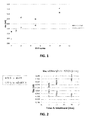
- Figure 1 shows the open-circuit voltage (Voc) of thin-film photovoltaic solar cells made of amorphous silicon with respect to the number of MVD cycles used in the deposition of the Al2O3 interstitial film between the ⁇ p> a-Si:C:H layer and the ⁇ i> a-Si:C:H layer of the device. Results with and without a vapor water flush exposition before the MVD deposition are presented. Note that in this example the Al2O3 film does not have any opening; in consequence the poor transport of positive charge carriers towards the ⁇ p> a-Si:C:H layer induces a decrease of the conversion efficiency of the solar cell.
- Voc open-circuit voltage
- Figure 2 shows the open-circuit voltage (Voc) of thin-film photovoltaic solar cells made of microcrystalline silicon with respect to the duration of an argon plasma treatment applied at the front ZnO contact layer.
- Voc open-circuit voltage
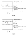
- a free electron-hole pair (e - -h + ) is photo-generated within the intrinsic absorber ( ⁇ i> a-Si:H layer) of a p-i-n solar cell deposited on a transparent substrate.
- the hole and the electron are under the influence of a random thermal movement (which on average is the cause of the diffusion currents of holes and electrons) and of the built-in electric field (E) produced by the ionized donors and acceptors of the ⁇ n> ⁇ c-Si:H and ⁇ p> a-Si:C:H layers, respectively (E is the cause of the drift currents of holes and electrons).
- E is the cause of the drift currents of holes and electrons.
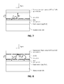
- Figure 5 shows an example of passivation at the p/i and i/n interfaces with additional negative fixed charges produced by the deposition of an Al2O3 interstitial film and with additional positive fixed charges produced by the deposition of a SiNx interstitial film, respectively, within a thin-film photovoltaic device of structure p-i-n made of amorphous silicon.
- the two interstitial films have openings at the nanometer scale.
- Interstitial film or interface treatment within an electronic or an optoelectronic device made of thin-film silicon and its alloys involves :
- Said interstitial film or said interface treatment involving a fixed positive charge allowing to decrease the recombination rate of free carriers of n type (electrons) at an interface having a side of n type within a device made of thin-film silicon and its alloys.
Landscapes
- Photovoltaic Devices (AREA)
Priority Applications (1)
| Application Number | Priority Date | Filing Date | Title |
|---|---|---|---|
| EP13199448.5A EP2887406A1 (fr) | 2013-12-23 | 2013-12-23 | Dispositif semi-conducteur et procédé de fabrication dudit dispositif semi-conducteur |
Applications Claiming Priority (1)
| Application Number | Priority Date | Filing Date | Title |
|---|---|---|---|
| EP13199448.5A EP2887406A1 (fr) | 2013-12-23 | 2013-12-23 | Dispositif semi-conducteur et procédé de fabrication dudit dispositif semi-conducteur |
Publications (1)
| Publication Number | Publication Date |
|---|---|
| EP2887406A1 true EP2887406A1 (fr) | 2015-06-24 |
Family
ID=49916916
Family Applications (1)
| Application Number | Title | Priority Date | Filing Date |
|---|---|---|---|
| EP13199448.5A Withdrawn EP2887406A1 (fr) | 2013-12-23 | 2013-12-23 | Dispositif semi-conducteur et procédé de fabrication dudit dispositif semi-conducteur |
Country Status (1)
| Country | Link |
|---|---|
| EP (1) | EP2887406A1 (fr) |
Cited By (1)
| Publication number | Priority date | Publication date | Assignee | Title |
|---|---|---|---|---|
| CN111668320A (zh) * | 2020-06-15 | 2020-09-15 | 中国科学院微电子研究所 | 硅漂移探测器及其加工方法 |
Citations (5)
| Publication number | Priority date | Publication date | Assignee | Title |
|---|---|---|---|---|
| US5370747A (en) * | 1991-11-25 | 1994-12-06 | Sanyo Electric Co., Ltd. | Photovoltaic device |
| US5719076A (en) * | 1996-04-24 | 1998-02-17 | United Solar Systems Corporation | Method for the manufacture of semiconductor devices with optimized hydrogen content |
| EP2077584A2 (fr) | 2007-12-28 | 2009-07-08 | Industrial Technology Research Institute | Structure de couche de passivation de cellule solaire et son procédé de fabrication |
| US20090283139A1 (en) | 2008-05-14 | 2009-11-19 | Miin-Jang Chen | Semiconductor structure combination for thin-film solar cell and manufacture thereof |
| WO2011160246A1 (fr) * | 2010-06-25 | 2011-12-29 | Oerlikon Solar Ag, Trübbach | Cellule solaire en film mince pourvue d'une couche absorbante microcristalline et d'une couche de passivation et son procédé de fabrication |
-
2013
- 2013-12-23 EP EP13199448.5A patent/EP2887406A1/fr not_active Withdrawn
Patent Citations (5)
| Publication number | Priority date | Publication date | Assignee | Title |
|---|---|---|---|---|
| US5370747A (en) * | 1991-11-25 | 1994-12-06 | Sanyo Electric Co., Ltd. | Photovoltaic device |
| US5719076A (en) * | 1996-04-24 | 1998-02-17 | United Solar Systems Corporation | Method for the manufacture of semiconductor devices with optimized hydrogen content |
| EP2077584A2 (fr) | 2007-12-28 | 2009-07-08 | Industrial Technology Research Institute | Structure de couche de passivation de cellule solaire et son procédé de fabrication |
| US20090283139A1 (en) | 2008-05-14 | 2009-11-19 | Miin-Jang Chen | Semiconductor structure combination for thin-film solar cell and manufacture thereof |
| WO2011160246A1 (fr) * | 2010-06-25 | 2011-12-29 | Oerlikon Solar Ag, Trübbach | Cellule solaire en film mince pourvue d'une couche absorbante microcristalline et d'une couche de passivation et son procédé de fabrication |
Non-Patent Citations (4)
| Title |
|---|
| A. RICHTER ET AL., PHYS. STATUS SOLIDI RRL, vol. 5, no. 5-6, 2011 |
| HOEX ET AL., J. APPL. PHYS., vol. 104, 2008, pages 113703 |
| VERMANG BART ET AL: "Improved Rear Surface Passivation of Cu(In,Ga)Se2 Solar Cells: A Combination of an Al2O3 Rear Surface Passivation Layer and Nanosized Local Rear Point Contacts", IEEE JOURNAL OF PHOTOVOLTAICS, I E E E, US, vol. 4, no. 1, 16 December 2013 (2013-12-16), pages 486 - 492, XP011535113, ISSN: 2156-3381, [retrieved on 20131219], DOI: 10.1109/JPHOTOV.2013.2287769 * |
| VERMANG ET AL., SOLAR ENERGY MATERIALS & SOLAR CELLS, vol. 117, 2013, pages 505 - 511 |
Cited By (1)
| Publication number | Priority date | Publication date | Assignee | Title |
|---|---|---|---|---|
| CN111668320A (zh) * | 2020-06-15 | 2020-09-15 | 中国科学院微电子研究所 | 硅漂移探测器及其加工方法 |
Similar Documents
| Publication | Publication Date | Title |
|---|---|---|
| NL2022817B1 (en) | Surface/interface passivation layer for high-efficiency crystalline silicon cell and passivation method | |
| US12426381B2 (en) | Tandem photovoltaic device and production method | |
| Mazzarella et al. | Nanocrystalline n-type silicon oxide front contacts for silicon heterojunction solar cells: photocurrent enhancement on planar and textured substrates | |
| KR102710224B1 (ko) | 전하-캐리어-선택적 접촉을 통해 연결되는 복수의 흡수체들을 구비한 태양 전지 | |
| EP3170209B1 (fr) | Cellule solaire à contact arrière interdigité | |
| US8395043B2 (en) | Solar cell comprising neighboring electrically insulating passivation regions having high surface charges of opposing polarities and production method | |
| US8350146B2 (en) | Three dimensional multi-junction photovoltaic device | |
| US20100132774A1 (en) | Thin Film Silicon Solar Cell Device With Amorphous Window Layer | |
| US20090314337A1 (en) | Photovoltaic devices | |
| WO2010104842A1 (fr) | Dispositifs photovoltaïques à semi-conducteurs multijonction et procédés pour leur fabrication | |
| Sui et al. | A review of technologies for high efficiency silicon solar cells | |
| US20150380581A1 (en) | Passivation of light-receiving surfaces of solar cells with crystalline silicon | |
| WO2017076832A1 (fr) | Dispositif photovoltaïque et son procédé de fabrication | |
| KR101072472B1 (ko) | 광기전력 장치의 제조 방법 | |
| WO2016049245A1 (fr) | Cellules solaires à contact passivé et procédés de fabrication | |
| JP2001267598A (ja) | 積層型太陽電池 | |
| US20100037940A1 (en) | Stacked solar cell | |
| CN103563091B (zh) | 具有改善的隧道结的串列太阳能电池 | |
| WO2014134515A1 (fr) | Cellules solaires à hétérojonction d'oxyde de zinc et de silicium à haute efficacité et à faible coût | |
| US20130095598A1 (en) | Back-surface field structures for multi-junction iii-v photovoltaic devices | |
| KR20100090015A (ko) | 태양전지 및 그 제조방법 | |
| Shu et al. | Alternative approaches for low temperature front surface passivation of interdigitated back contact silicon heterojunction solar cell | |
| EP2887406A1 (fr) | Dispositif semi-conducteur et procédé de fabrication dudit dispositif semi-conducteur | |
| Davis et al. | Engineered interfaces using surface and contact passivation in silicon solar cells | |
| KR101615611B1 (ko) | 터널링 다층 양자우물구조체를 이용한 태양전지 및 그 제조방법 |
Legal Events
| Date | Code | Title | Description |
|---|---|---|---|
| PUAI | Public reference made under article 153(3) epc to a published international application that has entered the european phase |
Free format text: ORIGINAL CODE: 0009012 |
|
| 17P | Request for examination filed |
Effective date: 20131223 |
|
| AK | Designated contracting states |
Kind code of ref document: A1 Designated state(s): AL AT BE BG CH CY CZ DE DK EE ES FI FR GB GR HR HU IE IS IT LI LT LU LV MC MK MT NL NO PL PT RO RS SE SI SK SM TR |
|
| AX | Request for extension of the european patent |
Extension state: BA ME |
|
| STAA | Information on the status of an ep patent application or granted ep patent |
Free format text: STATUS: THE APPLICATION IS DEEMED TO BE WITHDRAWN |
|
| 18D | Application deemed to be withdrawn |
Effective date: 20160105 |