EP2887787A2 - Kühlstruktur für Heizelement und Leistungswandler - Google Patents
Kühlstruktur für Heizelement und Leistungswandler Download PDFInfo
- Publication number
- EP2887787A2 EP2887787A2 EP14197340.4A EP14197340A EP2887787A2 EP 2887787 A2 EP2887787 A2 EP 2887787A2 EP 14197340 A EP14197340 A EP 14197340A EP 2887787 A2 EP2887787 A2 EP 2887787A2
- Authority
- EP
- European Patent Office
- Prior art keywords
- cooling
- heat
- heat receiving
- fins
- heating element
- Prior art date
- Legal status (The legal status is an assumption and is not a legal conclusion. Google has not performed a legal analysis and makes no representation as to the accuracy of the status listed.)
- Withdrawn
Links
- 238000001816 cooling Methods 0.000 title claims abstract description 339
- 238000010438 heat treatment Methods 0.000 title claims abstract description 57
- 230000005855 radiation Effects 0.000 claims abstract description 63
- 239000004065 semiconductor Substances 0.000 claims description 54
- 239000004519 grease Substances 0.000 claims description 13
- 230000003139 buffering effect Effects 0.000 claims description 5
- 125000006850 spacer group Chemical group 0.000 description 44
- 238000010586 diagram Methods 0.000 description 25
- 238000010992 reflux Methods 0.000 description 15
- 230000000694 effects Effects 0.000 description 14
- 239000003990 capacitor Substances 0.000 description 12
- 238000012986 modification Methods 0.000 description 11
- 230000004048 modification Effects 0.000 description 11
- 230000016507 interphase Effects 0.000 description 8
- 239000002826 coolant Substances 0.000 description 6
- 238000004519 manufacturing process Methods 0.000 description 6
- 230000003247 decreasing effect Effects 0.000 description 5
- 238000003475 lamination Methods 0.000 description 5
- 238000006243 chemical reaction Methods 0.000 description 4
- 239000007788 liquid Substances 0.000 description 4
- 230000000903 blocking effect Effects 0.000 description 3
- 238000009413 insulation Methods 0.000 description 3
- 238000000034 method Methods 0.000 description 3
- 238000004513 sizing Methods 0.000 description 3
- 230000007423 decrease Effects 0.000 description 2
- RYGMFSIKBFXOCR-UHFFFAOYSA-N Copper Chemical compound [Cu] RYGMFSIKBFXOCR-UHFFFAOYSA-N 0.000 description 1
- 229910052782 aluminium Inorganic materials 0.000 description 1
- XAGFODPZIPBFFR-UHFFFAOYSA-N aluminium Chemical compound [Al] XAGFODPZIPBFFR-UHFFFAOYSA-N 0.000 description 1
- 230000015572 biosynthetic process Effects 0.000 description 1
- 239000000919 ceramic Substances 0.000 description 1
- 239000006258 conductive agent Substances 0.000 description 1
- 239000004020 conductor Substances 0.000 description 1
- 239000000498 cooling water Substances 0.000 description 1
- 229910052802 copper Inorganic materials 0.000 description 1
- 239000010949 copper Substances 0.000 description 1
- 238000005520 cutting process Methods 0.000 description 1
- 238000010292 electrical insulation Methods 0.000 description 1
- 230000005669 field effect Effects 0.000 description 1
- 230000012447 hatching Effects 0.000 description 1
- 230000020169 heat generation Effects 0.000 description 1
- 239000012212 insulator Substances 0.000 description 1
- 238000012423 maintenance Methods 0.000 description 1
- 229910052751 metal Inorganic materials 0.000 description 1
- 239000002184 metal Substances 0.000 description 1
- 229910044991 metal oxide Inorganic materials 0.000 description 1
- 150000004706 metal oxides Chemical class 0.000 description 1
- 239000011347 resin Substances 0.000 description 1
- 229920005989 resin Polymers 0.000 description 1
- 239000010409 thin film Substances 0.000 description 1
- XLYOFNOQVPJJNP-UHFFFAOYSA-N water Substances O XLYOFNOQVPJJNP-UHFFFAOYSA-N 0.000 description 1
Images








Classifications
-
- H—ELECTRICITY
- H05—ELECTRIC TECHNIQUES NOT OTHERWISE PROVIDED FOR
- H05K—PRINTED CIRCUITS; CASINGS OR CONSTRUCTIONAL DETAILS OF ELECTRIC APPARATUS; MANUFACTURE OF ASSEMBLAGES OF ELECTRICAL COMPONENTS
- H05K7/00—Constructional details common to different types of electric apparatus
- H05K7/20—Modifications to facilitate cooling, ventilating, or heating
- H05K7/20009—Modifications to facilitate cooling, ventilating, or heating using a gaseous coolant in electronic enclosures
- H05K7/20136—Forced ventilation, e.g. by fans
- H05K7/20154—Heat dissipaters coupled to components
-
- H—ELECTRICITY
- H05—ELECTRIC TECHNIQUES NOT OTHERWISE PROVIDED FOR
- H05K—PRINTED CIRCUITS; CASINGS OR CONSTRUCTIONAL DETAILS OF ELECTRIC APPARATUS; MANUFACTURE OF ASSEMBLAGES OF ELECTRICAL COMPONENTS
- H05K7/00—Constructional details common to different types of electric apparatus
- H05K7/20—Modifications to facilitate cooling, ventilating, or heating
- H05K7/2089—Modifications to facilitate cooling, ventilating, or heating for power electronics, e.g. for inverters for controlling motor
- H05K7/20936—Liquid coolant with phase change
-
- H—ELECTRICITY
- H05—ELECTRIC TECHNIQUES NOT OTHERWISE PROVIDED FOR
- H05K—PRINTED CIRCUITS; CASINGS OR CONSTRUCTIONAL DETAILS OF ELECTRIC APPARATUS; MANUFACTURE OF ASSEMBLAGES OF ELECTRICAL COMPONENTS
- H05K7/00—Constructional details common to different types of electric apparatus
- H05K7/20—Modifications to facilitate cooling, ventilating, or heating
- H05K7/2029—Modifications to facilitate cooling, ventilating, or heating using a liquid coolant with phase change in electronic enclosures
- H05K7/20336—Heat pipes, e.g. wicks or capillary pumps
-
- H—ELECTRICITY
- H05—ELECTRIC TECHNIQUES NOT OTHERWISE PROVIDED FOR
- H05K—PRINTED CIRCUITS; CASINGS OR CONSTRUCTIONAL DETAILS OF ELECTRIC APPARATUS; MANUFACTURE OF ASSEMBLAGES OF ELECTRICAL COMPONENTS
- H05K7/00—Constructional details common to different types of electric apparatus
- H05K7/20—Modifications to facilitate cooling, ventilating, or heating
- H05K7/2039—Modifications to facilitate cooling, ventilating, or heating characterised by the heat transfer by conduction from the heat generating element to a dissipating body
- H05K7/20409—Outer radiating structures on heat dissipating housings, e.g. fins integrated with the housing
Definitions
- the present invention relates to a cooling structure for a heating element and a power converter.
- a power converter includes a circuit using semiconductor devices for performing current conduction and current blocking and provides functions of AC-DC conversion, frequency conversion, etc by controlling switching operations of the semiconductor devices.
- semiconductor devices in the power converter losses are generated upon current conduction and switching during turning on and off.
- a temperature of the semiconductor devices exceeds an operating limit point due to heat caused by the loss, current interruption cannot be done, so that the power converter cannot provide a desired operation. Accordingly, a cooling device for cooling the semiconductor devices is required in the power converter.
- JP 2013-73964 A discloses a semiconductor unit including a cooling device having two cooling surfaces, an electric terminal part, and a cooling unit with protrusions has a pin-shape.
- JP 2000-060106 A discloses, similarly to JP 2013-73964 A , a cooling device including a high heat conductor, and an air-cooling fins on two cooling surfaces.
- JP 2013-73964 A discloses, at a paragraph 0001,"the document relates to a power module having a high heat radiation characteristic and a high reliability and, at a paragraph 0011, "On one of the two confronting surfaces with larger area, is provided with a heat radiation part, and another surface has a heat radiation part".
- the heat radiation parts function as heat radiation walls for a module case 304.
- JP 2013-73964 A a cooling water is used for cooling the semiconductor devices.
- the power module housing the semiconductors therein has two surfaces for cooling the heat from their inside, each having a heat radiation part having a lot of fins on each of the surfaces, which may cause the structure to be complicated.
- JP 2000-060106 A an increase in the cooling characteristic has been tried by arranging a heat radiator near the semiconductor devices, etc.
- the structure becomes complicated. Accordingly, when this structure is applied to a power converter requiring a lot of power modules, a size of the power converter becomes large.
- the heating element such as the semiconductor module having originally designed as a water-cooling type.
- the use of the air-cooling type one eliminates necessity of piping for the coolant, which is advantageous to maintenance.
- the air-cooling type it becomes necessary to provide cooling fins, etc. having a certain size on the heating element.
- the heating element originally having designed as a water-cooling type one, has small pin fines (fins protruding in a pin shape), etc.
- such a heating element is designed without assumption that a large pressurizing force is applicable, so that there is no assumption that a strong pressure force is applied. Accordingly, when an external cooling fin is simply mounted by fastening bolts, the heating element may be damaged.
- An aspect of the present invention is to provide a cooling structure for a heating element or a plurality of power modules with extensibility in arranging the heating elements such as a power module and with down-sizing a device for power converters, etc., using the heating elements such as a plurality of power modules.
- An aspect of the present invention is to provide a cooling structure for a heating element, having pin fins and being capable of cooling the heating element for a semiconductor module, etc with avoidance of damage and a power converter.
- a first aspect of the present invention provides a cooling structure comprising; a plurality of heating elements arranged in a vertical direction, each including cooling surfaces respectively disposed on two confronting side surfaces extending in the vertical direction, and an electric terminal on a side surface extending the vertical direction and adjoining the two confronting side surfaces; a plurality of heat receiving blocks pinching the heating elements arranged in the vertical direction on the two confronting side surfaces; first and second cooling devices, each including a heat pipe including a plurality of heat radiation fins; a pressure contacting part configured to contact the heating elements and the receiving block with a pressure force; and a blower configured to apply a wind to the heat radiation fins.
- a second aspect of the present invention provides a cooling structure comprising: a heating element having at least a cooling surface including a plurality of protruded pin fins; a heat receiving plate having loose holes into which the pin fins are inserted at positions corresponding to the pin fins; a cooling device including pair of pinching members configured to pinch the heating element and the heat receiving plate with a pressure force and cool the heat receiving plate; and a space reserving part, disposed on the heat receiving plate, configured to control a gap (interval) in a pair of the pinching members so as not to apply a pressure force by the pinching members to the heating element.
- a cooling structure for a heating element has extensibility in arranging the heating element such as a power module and capability of down-sizing a device such as a power converters, etc., using the heating elements such as a plurality of power modules.
- the heating element can be cooled with avoidance of damage.
- a power converter 100 includes a plurality of single converter units 910 (see Figs. 9 and 12 ).
- the single converter unit 910 includes a double-sided-cooling power unit 520 (see Fig. 5 , semiconductor unit for the power converter) including a plurality of double-sided-cooling power modules 500 (semiconductor module, see Fig. 7 ). Respective components in the power converter 100 are described below.
- Fig 1 is a schematic circuit showing the power converter according to the first embodiment.
- the power converter 100 is supplied with an AC power having a voltage which is appropriately adjusted through a transformer 105 from a power receiving point 107 of a power grid.
- the supplied AC power is inputted into a converter 102 which converts the supplied AC power into a DC power.
- the DC power is inputted into the inverter 103 to convert the DC power into an AC power.
- the AC power is consumed by a three-phase AC load 108.
- an upper control circuit 109 detects this and controls a chopper 104 to operate.
- a DC power supplied from a battery 106 to the chopper 104 is adjusted to an appropriate power and inputted into an inverter 103.
- the DC power inputted into the inverter 103 is converted into an AC power which is consumed by the three-phase AC load 108.
- the operation described above is judged by the upper control circuit 109 as to whether the operation is a desired operation or not.
- the converter 102, the inverter 103, and the chopper 104 generate heat during their operations, so that temperatures increase.
- a cooling wind 111 is supplied to the converter 102, the inverter 103, and the chopper 104 by a cooling fan (blower) 101.
- the cooling fan 101, the converter 102, the inverter 103, the chopper 104, the upper control circuit 109, etc. are housed in the power converter 100 according to the embodiments.
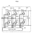
- Fig. 2 is a circuit diagram of the converter in the power converter.
- Fig. 3 is a circuit diagram of the inverter in the power converter.
- Fig. 4 is a circuit diagram showing the chopper in the power converter. With reference to Figs. 2 to Fig. 4 , circuits of the converter 102, the inverter 103, and the chopper 104 are described.
- the converter 102 shown in Fig. 2 includes leg 203s (203R, 203S, 203T) each configured with a plurality of semiconductor devices.
- the leg 203 includes a plurality of switching devices 204 (for example, 204RH, 204RL) and a plurality of diode devices 205 (for example, 205RH, 205RL).
- switching devices 204 for example, 204RH, 204RL
- diode devices 205 for example, 205RH, 205RL
- Both ends of the leg 203 are connected to a capacitor 201.
- An upper arm of the leg 203R includes a switching device 204RH and a refluxing diode device 205RH.
- a lower arm of a leg 203R includes a switching device 204RL and a refluxing diode device 205RL.
- an upper arm of the leg 203S includes a switching device 204SH and a refluxing diode device 205RH.
- a lower arm of the leg 203S includes a switching device 204SL and a refluxing diode device 205SL.
- An upper arm of a leg 203T includes a switching device 204TH and a refluxing diode device 205TH.
- a lower arm of the leg 203T includes a switching device 204TL and a refluxing diode device 205TL.
- Switching signals to the switching devices 204RH, 204RL, 204SH, 204SL, 204TH, 204TL are controlled by a converter gate controller 202, which is a lower control unit.
- any devices capable of turning on and off can be used.
- IGBT Insulated Gate Bipolar Transistor
- MOSFET Metal Oxide Semiconductor Field Effect Transistor
- the inverter 103 shown in Fig. 3 includes a plurality of the legs 203 (203U, 203V, 203W) configured with a plurality of semiconductor devices and both ends of the leg 203 are connected to a capacitor 301.
- the upper arm of the leg 203U includes a switching device 204UH and a refluxing diode 205UH.
- a lower arm of the leg 203U includes a switching device 204UL and a refluxing diode 205UL.
- an upper arm of a leg 203V includes a switching device 204VH and a refluxing diode 205VH.
- a lower arm of the leg 203V includes a switching device 204VL and a refluxing diode 205VL.
- An upper arm of a leg 203W includes a switching device 204WH and a refluxing diode 205WH.
- a lower arm of the leg 203W includes a switching device 204WL and a refluxing diode 205WL.
- Switching signal applied to the switching devices 204UH, 204UL, 204VH, 204VL, 204WH, 204WL are controlled by an inverter gate control unit 302 as a lower control part.
- the chopper 104 includes the leg 203 configured with semiconductor devices (203X). The both ends of the leg 203 are connected to a capacitor 401.
- An upper arm of a leg 203X includes a switching device 204XH and a refluxing diode 205XH.
- a lower arm of the leg 203 includes a switching device 204XL and a refluxing diode 205XL.
- a junction point between the switching devices 204XH and 204XL is connected to the battery 106 through a reactor 403 (see Fig. 1 ).
- the switching signals to the switching devices 204XH, 204XL are controlled by a chopper gate control unit 402.
- the chopper gate control unit 402 is amplified.
- the switching signals are applied to the chopper 104 through a boosting and stepping-down switching circuit (not shown). These selections depend on a larger-smaller relation in the output voltage of the converter 102 (commutation function).
- a PWM (Pulse Width Modulation) signal is transmitted to the switching device 204XL.
- the PWM signal is transmitted to the switching device 204XH.
- the switching device 204XL is switched in accordance with the PWM signal.
- an energy is stored in the reactor 403.
- the switching device turns off, due to the energy from the voltage of the battery 106 and the reactor 403, a voltage higher than the voltage of the battery 106 is charged in the capacitor 401 through the refluxing diode 205XH connected to the switching device 204XH.
- the switching device 204XH When the battery 106 is charged with an electric power, the switching device 204XH is switched in accordance with the PWM signal, so that an electric power in the capacitor 401 is charged in the battery 106 through the reactor 403 when the switching device 204XH is turned on. When the switching device 204XH is turned off, the energy stored in the reactor 403 is circulated through the diode 205XL connected to the switching device 204XL. The electric power in the battery 106 is charged and discharged by these operations.
- the capacitors may be arranged integrally.
- the capacitors 201, 301, 401 are divided from a point of view of standardizing the configuration of the single converter unit 910 (see Fig. 9 ) described later. More specifically, the capacitors 201, 301 are further divided for each of the legs 203.
- DC to AC conversion is performed and in the inverter 103, DC to AC conversion is performed by conducting and blocking of current by the switching device 204 and a diode 205 in the leg 203 shown in Figs. 2 to 4 .
- a loss is generated by the resistor in the switching device 204 and the diode device 205.
- a loss is generated. Accordingly, heat generation is caused by the operation of the power converter 100.
- Fig. 5 is a perspective view of the air-cooling type of double-sided-cooling power module in which a plurality of the double-sided-cooling power modules are disposed.
- Fig. 6 is an exploded view showing arrangement of the double-sided-cooling power modules in the air-cooling type of double-sided-cooling power unit.
- the air-cooling type of double-sided-cooling power unit 520 is configured to basically include a cooling device 510 (a first cooling device 510A, a second cooling device 510B) and a plurality of the double-sided-cooling power modules 500.
- the cooling device 510 includes a heat receiving block 501, a heat pipe 502, and a heat radiating fin 503.
- the first cooling device 510A includes a heat receiving block 501A, a heat pipe 502A, and a heat radiation fin 503A.
- the second cooling device 510B includes a heat receiving block 501 B, a heat pipe 502B, and a heat radiation fin 503B.
- the air-cooling type of double-sided-cooling power unit 520 has a slim and simple structure with such expandability that a plurality of power modules can be arranged in the actual structure of the double-sided-cooling power module 500.
- double-sided-cooling power modules 500 including semiconductor devices therein as a heat source
- the double-sided-cooling power module 500 and the heat receiving block 501 are fixed with bolts 504 and nuts 505 as a pressure-contacting means for providing pressure-contact therebeween.
- bolts 504 and nuts 505 Inside of the heat receiving block 501, one end of more than one heat pipe 502 are connected. The other ends of the heat pipe 502 extend upwardly and are connected to a plurality of the heat radiating fins 503 at parts protruding from the heat receiving blocks 501.
- a soft thermally conductive grease 506 (thermal conductive agent) having a high thermal conductivity is coated to reduce a poor heat contact caused by a roughness of respective surfaces and tolerance.
- Fig. 7A is a perspective view of the double-sided-cooling power module
- Fig. 7B is a schematic circuit diagram.
- the double-sided-cooling power module 500 includes a switching devices 204MH, 204ML, and diodes 205MH, 205ML. Respective semiconductors are connected to each other to form the leg 203 (for example, see Fig. 2 ).
- a P terminal 704P DC positive terminal
- an N-terminal 704N DC negative terminal
- an AC terminal 704AC AC terminal
- a gate terminal 701 are exposed at a top surface thereof to be connectable with an External with electrical insulation.
- electrical conduction to the external via these electric terminals electrical conduction to the external via these electric terminals.
- heat simultaneously generated is exhausted vie a cooling surface 702 being connected to an insulator 703. More specifically, the gate terminal 701 is electrically insulated from the cooling surface 702, and the heat transferring paths are independent from the electric path.
- the double-sided-cooling power module 500 includes: the cooling surfaces 702 on two confronting side surfaces and the P terminal 704P, a N terminal 704N, the AC terminal 704AC, and the gate terminal 701, which are electric terminals on one of the vertically extending side surfaces adjoining the cooling surface 702.
- Fig. 8 is an illustration showing a heat transferring path of the air-cooling type of double-sided-cooling power unit.
- Fig. 8 shows a cross section of a part in Fig. 5 .
- heat generated by semiconductor devices 802 included therein transfers to the heat pipe 502 through the heat receiving block 501, which rapidly transfers a heat 801 in the vertical direction.
- the heat 801 is transferred to the heat radiating fins 503 and exhausted by a cooling wind 803 flowing between the heat radiating fins 503.
- FIG. 9 is a perspective view of the single converter unit.
- Fig. 10 is an exploded view showing an arrangement of the single converter unit.
- Fig. 11 is a schematic circuit diagram of the single converter unit.
- the P terminal 704P, the N terminal 704N, the AC terminal 704AC which are electric terminals of the air-cooling type of double-sided-cooling power unit 520 (see Fig. 7 ), are connected to a P layer, an N layer, and an AC layer of a P • N • AC laminated bus bar 905, respectively.
- the gate terminal 701 which is an electric terminal, is connected to a gate driver circuit board 904.
- Positive terminals 902P and negative terminals 902N of a plurality of a capacitors 901 are connected to the P layer and the N layer of the P • N • AC laminated bus bar 905, respectively.
- a positive phase 903P and a negative phase 903N are connected to the P layer and the N layer of the P • N • AC laminated bus bar 905, respectively.
- Fig. 10 is an exploded view of the single converter unit 910 Fig. 9 .
- the P • N • AC laminated bus bar 905 includes a P bus bar 905P, an N bus bar 905N, and an AC bus bar 905AC which are electrically insulated each other with insulation layers (not shown).
- the P terminal 704P, the N terminal 704N, and the AC terminal 704AC of the double-sided-cooling power module are connected to the P bus bar 905P, the N bus bar 905N, and the AC bus bar 905AC, respectively.
- the gate terminal 701 of the double-sided-cooling power module 500 is connected to the gate driver circuit board 904. Further, the P terminal and the N terminal of the capacitor 901 are connected to the P bus bar 905P and the N bus bar 905N, respectively.
- the structure described above is shown in an electric circuit diagram as shown Fig. 11 .
- the cooling wind 803 is caused to flow to the heat radiating fin 503 from the side at which the electric terminals are installed.
- This structure provides such an advantageous effect that a cooling effect does not decrease among the single converter units 910 though the single converter units 910 are laterally arranged in the power converter 100 at a high density.
- the cooling wind comes from the side at which the terminals are installed.
- the present invention is not limited to this.
- the cooling wind may be caused to flow from a side opposite to the electric terminals to the heat radiating fins 503.
- Fig. 12 is an illustration showing the power converter in which a plurality of the single converter units are arranged.
- Fig. 13 is an illustration for illustrating a method of cooling the single converter units in the power converter.
- the converter 102, the inverter 103, and the chopper 104 are laterally arranged in the power converter 100.
- the converter 102 includes the single converter units 910 corresponding to the three legs 203R, 203S, 203T shown in Fig. 2 .
- the inverter 103 includes the single converter units 910 corresponding to three the legs 203U, 203V, 203V shown in Fig. 3 .
- the chopper 104 is shown in Fig. 4 with one of the legs 203X.
- the single converter unit 910 includes a circuit corresponding to the two legs 203X shown in Fig. 4 .
- the converter 102 is configured by connecting the three single converter units 910 by connecting a P • N interphase lamination bus bar 1003 to positive terminals 1001 and negative terminal 1002.
- the inverter 103 is configured similarly to the converter 102.
- the chopper 104 is configured by connecting the two single converter units 910 in parallel.
- a plurality of single converter units 907 may be connected in parallel for one leg. This can increase a rated output capacity of the power converter.
- the cooling wind 803 is caused to flow from the side of the electric terminals to the heat radiating fin 503. This provides such an advantageous effect that the cooling effect among the single converter units 910 is not decreased through the single converter units 910 are laterally arranged in the power converter 100 at a high density. Further, in the case where calorific values of of the converter 102, the inverter 103, and the chopper 104 are different from each other, velocities of cooling winds 803A, 803B, and 803C may be changed.
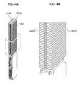
- Fig. 14A and 14B are perspective views in which the heat radiation fins of the first and second cooling devices are interlockingly arranged, in which Fig. 14A shows the whole view and Fig. 14B is an enlarged view.
- a heat radiating fin 1401A and a heat radiating fin 1401 B are different in height from the heat receiving blocks 501 A, 501 B and arranged interlockingly in which one fin of one of the first and second cooling device 510A and 510B is inserted into a space between the adjoining radiation fins of another of the first and second cooling device 510A and 510B.
- This is a difference of the heat radiating fin 503 shown in Fig. 14 from the heat radiating fin 503 shown in Fig. 5 .
- This structure has an advantageous effect in that heat radiation areas of the heat radiating fin 1401A and the heat radiating fin 1401 B are increased.
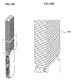
- Fig. 15A is a perspective view of the radiation fins in the case where the same radiation fins are installed at the heat pipes of the first and second cooling devices in which Fig. 15A shows the whole view and Fig. 15B is an enlarged view.
- a radiation fin 1501 in Fig. 15 is different from the heat radiating fin 503 shown in Fig. 5 in that the same heat radiation fins are used for both of the first cooling device 510A and the second cooling device 510B. Even in a case where calorific values are different from each other between a side of the first and second cooling devices 510A, 510B. This provides an advantageous effect in that the calorific values can be equalized with the same radiation fins.
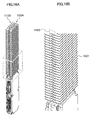
- Fig. 16A is a perspective view in a case where the radiation fins of the first and second cooling devices are connected with a waved rigid buffering part in which Fig. 16A shows the whole view and Fig. 16B is an enlarged view.
- heat radiating fins 1601 shown in Fig. 16 are connected between the first cooling device 510A and the second cooling device 510B with waved stiffness buffering parts 1602. This is a difference from the heat radiating fin 503 shown in Fig. 5 .
- This provides an advantageous effect in that the air-cooling type of double-sided-cooling power unit 520 configured to include the first cooling device 510A and the second cooling device 510B can increase a mechanical strength of the air-cooling type of double-sided-cooling power unit 520.
- a semiconductor unit for a power converter according to the embodiment (for example, the air-cooling type of double-sided-cooling power unit 520) includes:
- This provides an advantageous effect in expandability of arrangement of the double-sided-cooling power module 500 and down-sizing the air-cooling type of double-sided-cooling power unit 520 using a plurality of the air-cooling type of double-sided-cooling power unit 520.
- the air-cooling type of double-sided-cooling power unit 520 shown in Fig 5 has been described about assembling the two double-sided-cooling power modules 500.
- the present invention is not limited to this.
- the double-sided-cooling power modules 500 are arranged in a vertical direction. However, more than two double-sided-cooling power modules 500 may be arranged.
- the semiconductor unit for the power converter includes cooling surface confronting each other, more than one double-sided-cooling semiconductor modules having electric terminal part electrically insulated therein, and the cooling device 510 (heat radiator) sandwiching the double-sided-cooling semiconductor modules from both sides thereof.
- the cooling device 510 includes a member called the heat receiving block 501 having flat surfaces, the heat pipe 502, and the heat radiating fin 503.
- Semiconductor unit for the power converter is characterized by having expandability of arrangement of the double-sided-cooling power module, and a slim and simple structure.
- the heat pipe 502 straightly extends in a direction in parallel to the flat surface of the heat receiving block 501.
- One end of the heat pipe 502 is embedded in the heat receiving block 501 and the other end extends outwardly from the heat receiving block 501.
- the heat pipe 502 extending from the heat receiving block 501 is connected to the heat radiating fin 503.
- the heat generated by the semiconductor device 802 can be rapidly dispersed via the heat pipe 502 and transmitted to the heat radiating fin 503 , so that an efficiency of the heat radiation fin can be increased. Further, connection between the cooling device 510 and the double-sided-cooling semiconductor module is made through the heat receiving block 501. Accordingly, for example, this allows a defected double-sided-cooling semiconductor module to be easily replaced.
- Fig. 17 is a schematic circuit diagram of the power converter 150 according to the second embodiment.
- the power converter 150 is different from the power converter 100 in the first embodiment (see Fig. 1 ) in that a converter 152, an inverter 153, a chopper 154 are used in place of the converter 102, the inverter 103, and the chopper 104. Other parts are similarly configured.
- a filter circuit may be disposed between the converter 152 and the transformer 105 or between the inverter 153 and the three-phase AC load 108.
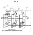
- Fig. 18 is a schematic circuit diagram of the converter 152.
- Fig. 19 is a schematic circuit diagram of the inverter 153.
- Fig. 20 is a schematic circuit diagram of the chopper 154.
- the converter 152, the inverter 153, and the chopper 154 have the same circuit structure as the converter 102, the inverter 103, and the chopper 104 (see Figs. 2 to 4 ), respectively except that a leg 253 is used in place of the leg 203.
- the circuit structure of the leg 253 is similar to the leg 203.
- an exterior appearance of the leg 253 is different from that of the leg 203, and exterior appearances of the converter 152, the inverter 153, and the chopper 154 are different from those of the converter 102, the inverter 103, and the chopper 104 in the first embodiment, respectively. These differences are described later.
- an air-cooling type of double-sided-cooling power unit 600 (heating body, a semiconductor unit for the power converter) used in the second embodiment is described with reference to the perspective view in Fig. 21A and a schematic circuit diagram in Fig. 21B .
- Each of the semiconductor devices is connected to configure the leg 253 (for example, see Fig. 18 ).
- Attached to an insulation body 753 are a P terminal 754P (DC positive terminal), an N terminal 754N (DC negative terminal), an AC terminal 754AC (AC terminal), and a gate terminal 751 for controlling switching between tuning-on and turning off.
- the air-cooling type of double-sided-cooling power unit 600 includes a cooling body 710 having a substantially rectangular parallelepiped, a flange 720, and on the flange 720, a terminal part 730 having a plurality of terminals extending from a surface opposite to the cooling body 710.
- the terminals in the terminal part 730 includes the P terminal 754P, the N terminal 754N, the AC terminal 754AC, and the gate terminal 751 which are shown in Fig. 21B .
- pin fins 762 Protruding from a one surface 760A of the cooling body 710 are a lot of (a total is not smaller than 200) pin fins 762 each having a small column shape. Further, formed on the other surface 760B opposite to the surface 760A are the same number of pin fins 762B (see Fig. 25 ). Hereinafter, the pin fins 762A and the pin fins 762B may be integrally referred to simply as "pin fin 762".
- the air-cooling type of double-sided-cooling power unit 600 is assumed to be cooled by a water cooling system.
- the terminal part 730 is directed upwardly and the cooling body 710 is directed downwardly, so that the cooling body 710 can be immersed into a cooling vessel to allow a coolant to flow between the pin fins 762.
- the surfaces 760A, 760B are called “cooling surface”. It is assumed that a thickness of the cooling body 710, i.e., a distance between the surface 760A d the the other surface 760B, is "d1 ".
- the terminal part 730 When the semiconductor devices operate, electric connection to the external is provided via the terminal part 730. On the other hand, heat exhausting is provided via the surface 760A, 760B. More specifically, the terminal part 730 is formed on one of the side surface adjoining to the surfaces 760A, 760B and is electrically insulated from the surfaces 760A, 760B. Accordingly, the heat transfer path is independent from the electric paths.
- the heat receiving spacer 630A includes a heat receiving part 631A (heat receiving plate) and a pair of space abutting parts 632A, having a substantially rectangular parallelepiped, protruding from the both ends of the heat receiving part 631A toward a heat receiving spacer 630B. Further, the heat receiving part 631A has a lot of loose through holes 633A having a circular column shape.
- These loose through holes 633A are formed at corresponding positions facing a cooling surface pin fins 762A on the surface 760A and have a diameter which is slightly greater than a diameter of the pin fins 762A. Essentially, it is ideal that the loose through holes 633A fit into the pin fins 762A tightly without any gap. However, there are slight errors caused during manufacturing regarding a diameter and a position of the pin fin 762A. Accordingly, a diameter of the through hole 633A is expanded to such an extent that the manufacturing error can be absorbed.
- the heat receiving spacer 630B includes the heat receiving part 631 B having a substantially rectangular parallelepiped shape and a space reserving part 632B having a substantially rectangular parallelepiped extends from both ends of a heat receiving part 631 B having a substantially rectangular parallelepiped.
- the heat receiving spacer 630B has a symmetrical shape about the heat receiving spacer 630A.
- the heat receiving part 631 B has loose through holes 633B at position corresponding to the pin fins 762 protruding from the the other surface 760B of the air-cooling type of double-sided-cooling power unit 600, respectively.
- Fig. 25 shows the state in which the heat receiving spacer 630A, 630B are attached, as described above, to the air-cooling type of double-sided-cooling power unit 600. As shown, an end surface 710a thereof of the cooling body 710 is exposed. However, large parts of the surfaces 760A, 760B are covered by the heat receiving spacers 630A, 630B.
- FIG. 24 An enlarged plan view of a part B in Fig. 23 , which is enclosed with a broken line is shown in Fig. 24 .
- a diameter of the loose through hole 633A is slightly greater than that of the pin fin 762A, so that the pin fin 762A is inserted into the gap 635 the pin fin 762A provide a gap 635 with the loose through hole 633A During this, the thermally conductive grease coated on the pin fin 762A is pushed into and penetrates into the gap 635, so that the gap 635 is filled with the thermally conductive grease.
- Fig. 25 shows an enlarged view of a main part (end part) taken along line A -A' in Fig. 23 .
- the heat receiving part 631A faces the heat receiving part 631 B through a predetermined distance. This distance is d2 (see Fig. 25 ).
- the heat receiving spacer 630A, 630B are formed so that a distance d2 is greater than a thickness d1 of the cooling body 710 of the air-cooling type of double-sided-cooling power unit 600.
- gaps 637A, 637B are formed between the heat receiving part 631A and the cooling body 710 and between the heat receiving part 631 B and the cooling body 710. Because the air-cooling type of double-sided-cooling power unit 600 has play with the heat receiving spacer 630A, 630B, widths of the gap 637A 637B are not the same.
- the thermally conductive grease coated on the pin fin 762 is pushed and penetrates into the gap 637A, 837B, so that the gap 637A, 637B are also filled with the thermally conductive grease without generation of gaps.
- a thickness of the cooling body 710 including a tip of the pin fin 762A to the tip of the pin fin 762B is d4
- a width of the whole body when the heat receiving spacer 630A is abutted on the heat receiving spacer 630B is d5
- the heat receiving spacers 630A, 630B are formed such that the width d5 is slightly greater than a thickness d4. Accordingly, gaps 639A, 639B are formed between the an upper surface of the heat receiving spacer 630A and the tip of the pin fin 762A, and between a lower surface of the heat receiving spacer 630B and the tip of the pin fin 762B.
- the air-cooling type of double-sided-cooling power unit 600 has play on the heat receiving spacers 630A, 630B, so that widths of the gap 637A, 637B are not the same.
- a pressure force as shown by an arrow with hatching is applied.
- the pressure force is applied to the abutting part between the space reserving part 632A, 632B.
- the gaps 637A, 637B are formed between the cooling body 710 and the heat receiving spacers 630A, 630B and the gaps 639A, 639B are formed at tips of the pin fins 762A, 762B. This prevents that the pressure force is applied to the cooling body 710. This can previously prevents the air-cooling type of double-sided-cooling power unit 600 from being defected.
- Fig. 26 shows a perspective view in which the the air-cooling type of double-sided-cooling power unit 600 is attached to the cooling device 610.
- the cooling device 610 includes a pair of cooling devices 610A, 610B.
- the cooling device 610A, 610B includes heat receiving blocks 601 A, 601 B, each being formed in a block in a substantially rectangular parallelepiped.
- the air-cooling type of double-sided-cooling power unit 600 is sandwiched.
- the heat receiving blocks 601 A, 601 B are fastened by a plurality of fixing members 604 each other.
- the pressure forces indicated with hatched arrows are applied to the heat receiving blocks 601A, 601 B.
- the pressure force is applied to the heat receiving spacers 630A, 630B, but not applied to the air-cooling type of double-sided-cooling power unit 600.
- the fixing member 604 well-known bolts and nuts are usable.
- FIG. 26 four heat pipes 602 protrude in a y-axis direction from the heat receiving block 601A with inclination of about 10 degrees from the xy plane (horizontal plane) defined by the X, y axes.
- a plurality of a heat radiation fins 603 having plate shapes are welded thereon in a radial direction of the heat pipe 602. Accordingly, the heat radiation fins 603 are inclined from the xz plane (vertical plane) defined by the x axis and the z axis.
- a cooling device 610B is also configured similarly to the cooling device 610A. As described above, the two air-cooling type of double-sided-cooling power units 600 are attached to the cooling device 610, so that the air-cooling type of double-sided-cooling power unit 620 is configured.
- the heat is transferred to the heat receiving blocks 601 A, 601 B and further transferred to a rear part (in a direction of y-axis) by the heat pipe 602.
- a cooling wind 853 is applied to the air-cooling type of double-sided-cooling power unit 620 so as to flow upwardly (in the z-axis direction) from a lower part of the air-cooling type of double-sided-cooling power unit 620, the cooling wind 853 cools the heat radiation fins 603 and passes there upwardly, so that the heat is rapidly exhausted.
- the heat transferring path is shown with arrows 851 in Fig. 26 . Further, heat transferring in a direction orthogonal with the cooling wind 853 is mainly generated by the heat pipe 602.
- FIG. 26 an exploded view of the region C encircled with a broken line is shown in Fig. 27 .
- the a conductive grease 606 is coated between the heat receiving spacer 630A and the heat receiving block 601A and between the heat receiving spacer 630B and the heat receiving spacer 630B, respectively.
- the thermally conductive grease 606 spreads along confronting surfaces between the heat receiving spacer 630A and the heat receiving block 601A and surfaces between the heat receiving spacer 630B and a heat receiving block 601 B so as to be in a thin film state.
- the thermally conductive grease 606 also penetrates into the gaps 639A, 639B (see Fig. 25 ) and penetrates on outer surface of the pin fins 762A, 762B without any gap.
- Fig. 28 is a perspective view of the single converter unit 960.
- Fig. 29 is an exploded view of the single converter unit 960.
- Fig. 30 is an exploded view of a P • N • AC laminated bus bar 955.
- Fig. 31 is a schematic circuit diagram of the single converter unit 960.
- the P terminal 754P (see Fig. 21 ), the N terminal 754N, and the AC terminal 754AC, being electric terminals of the air-cooling type of double-sided-cooling power unit 620 described above, are connected to the P layer, the N layer, and the AC layer of the P • N • AC laminated bus bar 955, respectively.
- the gate terminal 751 of an electric terminal is connected to a gate driver circuit board 954.
- positive terminals 952P and negative terminals 952 of a plurality of capacitors 951 are connected to the P layer and the N layer of the P • N • AC laminated bus bar 955, respectively.
- positive fuses 953P and negative fuses 953N are connected to the P layer and the N layer of the P • N • AC laminated bus bar 955, respectively.
- the positive fuse 953P and the negative fuse 953N have functions for cutting off the circuits to protect devices which an over current flows therethrough. If such a protection function is unnecessary, it is possible to omit the fuses.
- Fig. 29 is an exploded view of Fig. 28 .
- Fig. 30 is an exploded view of the P • N • AC laminated bus bar 955.
- the P • N • AC laminated bus bar 955 includes a P layer bus bar 955P, the P layer bus bar 955P, an N layer bus bar 955N, an N • AC layer bus bar 955C.
- the P terminal 754P, the N terminal 754N, the AC terminal 754AC are connected to the P layer bus bar 955P, the N layer bus bar 955N, and an AC bus bar 955AC, and the AC bus bar 955AC, respectively.
- the P terminal and the N terminal of the capacitor 951 are connected to the P layer bus bar 955P and the N layer bus bar 955N, respectively.
- the configuration in a circuit diagram described above is as shown in Fig. 31 .
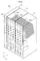
- Fig. 32 is a perspective view of the power converter 150 in which a plurality of the single converter units 960 are arranged.
- the converter 152 includes the single converter units 960 corresponding to the three legs 253R, 253S, and 253T shown in Fig. 18 .
- the inverter 153 includes the single converter units 960 corresponding to the three legs 253U, 253V, and 253W, as shown in Fig. 19 .
- the chopper 154 includes the one single converter unit 960.
- the converter 152, the inverter 153, the chopper 154 can be arranged in an order which is different from the embodiment of the present invention, and the converters 152, the inverters 153, and the choppers 154 may be arranged thereamong in a different phase order.
- the heat generated by the air-cooling type of double-sided-cooling power unit 600 is transferred to a rear side (in the y direction) with the heat pipe 602 and exhausted through the heat radiation fins 603 provided at a rear part.
- a plurality of the single converter units 960 in which the air-cooling type of double-sided-cooling power units 620 are installed are arranged in a lateral direction, so that maintainability can be increased.
- the unit in traveling is drawn out from the power converter 150 and a spare unit is inserted. During this, drawing out the traveled unit and inserting a spare unit can be provided by moving these units simply in the y direction, so that a rapid maintain ace operation can be provided.
- the converter 152 is configured by connecting the three single converter units 960 by connecting the P • N interphase lamination bus bar 1053 to corresponding positive terminals 1051 and negative terminals 1052.
- the inverter 153 and the converter 152 are similarly configured. Because the chopper 154 includes the one single converter unit 960, it is not always necessary that the chopper 154 is connected to the P • N interphase lamination bus bar 1053. However, if a capacity of the chopper 154 is increased or in a case where the converter 152 and the inverter 153 are configured as an integrated system as describe in the second embodiment, it is desirable to connect the converter 152 and the inverter 153 at the same time.
- the P • N interphase lamination bus bar 1053 includes, as shown in Fig. 33 , an interphase P bus bar 1053P and an interphase N bus bar 1053N, in which a insulating layer 105S provides insulation between respective bus bars.
- the converter 152 In the converter 152, the inverter 153, and the chopper 154, it is also possible to connect a plurality of the single converter units 960 in parallel for each leg. Accordingly, the rated output capacity of the power converter can be increased.
- the cooling wind 853 is applied to the heat radiation fins 603 from a lower side to upper side. Accordingly, through the single converter unit 960s are arranged in the power converter 150 in lateral direction at a high density, the cooling efficiency between respective the single converter unit 960 cannot be decreased as an advantageous effect. In a case where temperatures of semiconductor devices in the converter 152, the inverter 153, and the chopper 154 are different, velocity of cooling winds 853A, 853B, 853C may be changed.
- a cooling structure including: a heating element 600 having at least a cooling surface 760A, 760B including a plurality of protruded pin fins 762; a heat receiving plate 631A, 631 B having loose holes 633A, 633B into which the pin fins 762 are inserted at positions corresponding to the pin fins 762; a cooling device 610 including pair of pinching members 601 A, 601 B configured to pinch the heating element 600 and the heat receiving plate 631A, 631B with a pressure force and cool the heat receiving plate 631A, 631B; and a space reserving part 632A, 632B, disposed on the heat receiving plate 631A, 631 B, configured to control a gap (interval) in a pair of the pinching members 601A, 601 B so as not to apply a pressure force by the pinching members 601 A, 601 B to the heating element 600.
- the heat in the air-cooling type of double-sided-cooling power unit 600 can be transferred and cooled through the heat receiving parts 631A, 631 B and the heat receiving blocks 601A, 601 B.
- the air-cooling type of double-sided-cooling power unit 600 as the heating element includes cooling surfaces 760A, 760B on two confronting surfaces.
- the heat receiving plates 631A, 631 B have a shape corresponding to the cooling surfaces 760A, 760B and loose holes at positions corresponding to the pin fins 762. This provides transferring the heat from the double-sided cooling surfaces, so that the heat transferring effect can be further increased.
- thermally conductive grease 606 is coated between the pin fins 762 and a heat receiving plates 631A, 631 B. Accordingly, a thermal resistance between the heating element and the heat receiving parts 631A, 631 B can be reduced, so that the cooling device 610 can be down-sized.
- the space reserving part 632A, 632B control the interval (d5 + width of the thermally conductive grease 606) between a pair of pinching members (the heat receiving blocks 601A, 601 B) is larger than a thickness d4 of the heating element including the pin fins 762. Accordingly, when the pinching members pinch the heating element, application of the pressure force to the pin fins 762 and defection of the heating elements is prevented.
- the power converter 150 side surfaces of a plurality of semiconductor units for the power converter are arranged on the same plane, and a cooling wind is supplied by the cooling fan 101 to a plurality of heat radiation fins 603 from a rear side of the same plane. Accordingly, wiring between the air-cooling type of double-sided-cooling power unit 600 can be provided by the P • N interphase lamination bus bar 1053.
- a pair of a space reserving part 652 having a rectangular parallelepiped are formed so as pinch the region where the hollow part 654B is formed.
- parts corresponding to the space reserving part 652 are not formed.
- the space reserving part 652 are formed to be lower than the thickness d4 (see Fig. 25 ) of the cooling body 710 including the pin fin 762 and slightly higher than the thickness d1 of the cooling body 710 except the pin fin 762 (see Fig. 25 ).
- a depth of the hollow part 654B formed in the heat receiving block 650B and a depth of the hollow part (not shown) formed in the heat receiving block 650A are slightly deeper than a height of the pin fin 762. Accordingly, in Fig. 37 , though the air-cooling type of double-sided-cooling power unit 600 is pinched between the heat receiving blocks 650A 650B and the heat receiving blocks 650A, 650B are fasten with the fixing members 604, a pressure force is not applied to the air-cooling type of double-sided-cooling power units 600.
- the heat receiving blocks 650A, 650B have the functions of the heat receiving spacers 630A, 630B and the heat receiving blocks 601A, 601 B together. Further, the number of the components can be reduced, so that there are advantageous effects in that the manufacturing control can be easily provided. In addition, there is not always to form the the space reserving part 652 in the modification together with the heat receiving block 650B but may be formed separately.
- Fig. 38 shows an example of this structure as a modification.
- Flow channels 1601 are formed in the heat receiving block 601 B.
- One end of a forward pipe 1602A is connected to one end of each of the flow channels 1601.
- the forward pipe 1602A is connected to one end of a return pipe 1603.
- the other end of the return pipe 1603 is connected to one end of the backward pipe 1602B.
- the other end of the backward pipe 1602B is connected to the other end of the flow channels 1601 to form a flow path 1604.
- the heat of the heating element is transferred to a liquid coolant (not shown) in the flow channel 1601 in the heat receiving block 601 B.
- the liquid coolant flows and circulates through the flow path 1604, so that the heat in the liquid coolant is radiated by the heat radiation fins 603.
- the heat receiving block 601 B has a pair of this structure.
- the heat receiving block 601A also has a pair of this structure.
- the air-cooling type of double-sided-cooling power unit 520 in the first embodiment also can have this structure.
Landscapes
- Engineering & Computer Science (AREA)
- Microelectronics & Electronic Packaging (AREA)
- Physics & Mathematics (AREA)
- Thermal Sciences (AREA)
- Inverter Devices (AREA)
- Cooling Or The Like Of Electrical Apparatus (AREA)
Applications Claiming Priority (2)
| Application Number | Priority Date | Filing Date | Title |
|---|---|---|---|
| JP2013257945A JP2015115523A (ja) | 2013-12-13 | 2013-12-13 | 電力変換装置用半導体装置および電力変換装置 |
| JP2014198049A JP5805838B1 (ja) | 2014-09-29 | 2014-09-29 | 発熱体の冷却構造、電力変換器ユニットおよび電力変換装置 |
Publications (2)
| Publication Number | Publication Date |
|---|---|
| EP2887787A2 true EP2887787A2 (de) | 2015-06-24 |
| EP2887787A3 EP2887787A3 (de) | 2015-08-19 |
Family
ID=52272828
Family Applications (1)
| Application Number | Title | Priority Date | Filing Date |
|---|---|---|---|
| EP14197340.4A Withdrawn EP2887787A3 (de) | 2013-12-13 | 2014-12-11 | Kühlstruktur für Heizelement und Leistungswandler |
Country Status (2)
| Country | Link |
|---|---|
| US (1) | US9497887B2 (de) |
| EP (1) | EP2887787A3 (de) |
Cited By (3)
| Publication number | Priority date | Publication date | Assignee | Title |
|---|---|---|---|---|
| CN111816630A (zh) * | 2020-06-30 | 2020-10-23 | 科华恒盛股份有限公司 | 一种散热结构及功率模块 |
| CN112213906A (zh) * | 2020-09-30 | 2021-01-12 | 青岛海信激光显示股份有限公司 | 一种投影设备及投影系统 |
| CN118906880A (zh) * | 2024-08-22 | 2024-11-08 | 江西瑞华智能科技有限公司 | 一种模块化设计充电桩 |
Families Citing this family (14)
| Publication number | Priority date | Publication date | Assignee | Title |
|---|---|---|---|---|
| WO2016139763A1 (ja) * | 2015-03-04 | 2016-09-09 | 株式会社日立製作所 | 電力変換ユニットおよび電力変換装置 |
| CN106298688B (zh) * | 2015-05-28 | 2018-11-06 | 台达电子工业股份有限公司 | 封装型功率电路模块 |
| US9733680B1 (en) * | 2016-03-16 | 2017-08-15 | Microsoft Technology Licensing, Llc | Thermal management system including an elastically deformable phase change device |
| JP6649854B2 (ja) * | 2016-07-21 | 2020-02-19 | レノボ・シンガポール・プライベート・リミテッド | 電子機器 |
| US9955613B2 (en) * | 2016-09-13 | 2018-04-24 | Denso International America, Inc. | Cooler and power electronic module having the same |
| US10181674B1 (en) * | 2017-08-09 | 2019-01-15 | Phoenix Contact Development and Manufacturing, Inc. | Composite electrical connector system |
| CN108281403B (zh) * | 2018-02-28 | 2020-04-10 | 爱美达(上海)热能系统有限公司 | 一种用于冷却储存模块的多孔流道液冷板 |
| DE102018217981A1 (de) * | 2018-10-22 | 2020-04-23 | Volkswagen Aktiengesellschaft | Wechselrichtereinrichtung und Kraftfahrzeug mit einer Solchen |
| US12107032B2 (en) * | 2018-12-19 | 2024-10-01 | Abb Schweiz Ag | Cooling of power semiconductors |
| JP7030734B2 (ja) | 2019-03-04 | 2022-03-07 | 株式会社日立製作所 | 半導体装置 |
| US11224147B1 (en) * | 2020-11-19 | 2022-01-11 | GM Global Technology Operations LLC | Direct cooling of inverter switches |
| US12193202B2 (en) | 2021-09-15 | 2025-01-07 | Marel Power Solutions, Inc. | Air cooled compact power systems |
| CA3231013A1 (en) | 2021-09-15 | 2023-03-23 | Marel Power Solutions, Inc. | Air-cooled power converter |
| CN114710945B (zh) * | 2022-06-07 | 2022-08-16 | 广东电网有限责任公司广州供电局 | 一种配电变压器绕组加热头的快速散热装置及方法 |
Citations (2)
| Publication number | Priority date | Publication date | Assignee | Title |
|---|---|---|---|---|
| JP2000060106A (ja) | 1998-08-14 | 2000-02-25 | Toshiba Corp | 電力変換装置 |
| JP2013073964A (ja) | 2011-09-26 | 2013-04-22 | Hitachi Automotive Systems Ltd | パワーモジュール |
Family Cites Families (28)
| Publication number | Priority date | Publication date | Assignee | Title |
|---|---|---|---|---|
| US3536960A (en) * | 1968-06-26 | 1970-10-27 | Electric Regulator Corp | Heat sink module |
| JP3700870B2 (ja) * | 1995-10-26 | 2005-09-28 | 古河電気工業株式会社 | 車両における筐体内の電気部品冷却装置 |
| EP2234154B1 (de) * | 2000-04-19 | 2016-03-30 | Denso Corporation | Kühlmittelgekühlte Halbleiteranordnung |
| CA2408286C (en) * | 2000-05-08 | 2009-01-06 | Siemens Aktiengesellschaft | Control device |
| US6483705B2 (en) * | 2001-03-19 | 2002-11-19 | Harris Corporation | Electronic module including a cooling substrate and related methods |
| US7068507B2 (en) * | 2002-09-27 | 2006-06-27 | Rockwell Automation Technologies, Inc. | Compact liquid converter assembly |
| JP4154325B2 (ja) * | 2003-12-19 | 2008-09-24 | 株式会社日立産機システム | 電気回路モジュール |
| US20050207134A1 (en) * | 2004-03-16 | 2005-09-22 | Belady Christian L | Cell board interconnection architecture |
| US7165413B2 (en) * | 2004-07-09 | 2007-01-23 | Symons Robert S | Integrated liquid cooling device with immersed electronic components |
| US20060018100A1 (en) * | 2004-07-21 | 2006-01-26 | Yunxing Guo | Active plate-connector device with built-in semiconductor dies |
| JP4009630B2 (ja) | 2004-10-01 | 2007-11-21 | 埼玉日本電気株式会社 | 放熱部材の押さえ金具及び電子デバイスの放熱構造 |
| JP2007066480A (ja) * | 2005-09-02 | 2007-03-15 | Hitachi Ltd | ディスクアレイ装置 |
| US7324341B2 (en) * | 2005-09-22 | 2008-01-29 | Delphi Technologies, Inc. | Electronics assembly and heat pipe device |
| US7515423B2 (en) * | 2006-09-22 | 2009-04-07 | Fu Zhun Precision Industry (Shen Zhen) Co., Ltd. | Heat dissipation device |
| JP5028085B2 (ja) * | 2006-12-27 | 2012-09-19 | アイシン・エィ・ダブリュ株式会社 | 電子回路装置とその製造方法 |
| DE102007030389B4 (de) * | 2007-03-30 | 2015-08-13 | Rogers Germany Gmbh | Moduleinheit mit einer Wärmesenke |
| US20090129024A1 (en) * | 2007-11-15 | 2009-05-21 | Dennis Mahoney | Inverted through circuit board mounting with heat sink |
| WO2009150875A1 (ja) * | 2008-06-12 | 2009-12-17 | 株式会社安川電機 | パワーモジュールおよびその制御方法 |
| EP2328172B1 (de) * | 2009-10-02 | 2019-06-26 | Abb Research Ltd. | Leistungselektronikanordnung |
| US8189324B2 (en) * | 2009-12-07 | 2012-05-29 | American Superconductor Corporation | Power electronic assembly with slotted heatsink |
| JP2011167049A (ja) * | 2010-02-15 | 2011-08-25 | Denso Corp | 電力変換装置 |
| JP5500718B2 (ja) * | 2010-03-05 | 2014-05-21 | 株式会社ケーヒン | 半導体装置 |
| US9003649B1 (en) * | 2010-06-25 | 2015-04-14 | Maxq Technology, Llc | Method of making a two-sided fluid cooled assembly |
| US8218320B2 (en) * | 2010-06-29 | 2012-07-10 | General Electric Company | Heat sinks with C-shaped manifolds and millichannel cooling |
| JP5206822B2 (ja) * | 2010-07-09 | 2013-06-12 | 株式会社デンソー | 半導体装置 |
| KR101189451B1 (ko) * | 2010-12-24 | 2012-10-09 | 엘지전자 주식회사 | 인버터 스택 |
| US8611091B2 (en) * | 2011-03-11 | 2013-12-17 | Asia Vital Components Co., Ltd. | Thermal module for solar inverter |
| KR101540146B1 (ko) * | 2012-06-22 | 2015-07-28 | 삼성전기주식회사 | 전력 모듈용 방열 시스템 |
-
2014
- 2014-12-11 EP EP14197340.4A patent/EP2887787A3/de not_active Withdrawn
- 2014-12-12 US US14/568,300 patent/US9497887B2/en not_active Expired - Fee Related
Patent Citations (2)
| Publication number | Priority date | Publication date | Assignee | Title |
|---|---|---|---|---|
| JP2000060106A (ja) | 1998-08-14 | 2000-02-25 | Toshiba Corp | 電力変換装置 |
| JP2013073964A (ja) | 2011-09-26 | 2013-04-22 | Hitachi Automotive Systems Ltd | パワーモジュール |
Cited By (4)
| Publication number | Priority date | Publication date | Assignee | Title |
|---|---|---|---|---|
| CN111816630A (zh) * | 2020-06-30 | 2020-10-23 | 科华恒盛股份有限公司 | 一种散热结构及功率模块 |
| CN112213906A (zh) * | 2020-09-30 | 2021-01-12 | 青岛海信激光显示股份有限公司 | 一种投影设备及投影系统 |
| CN112213906B (zh) * | 2020-09-30 | 2022-02-01 | 青岛海信激光显示股份有限公司 | 一种投影设备及投影系统 |
| CN118906880A (zh) * | 2024-08-22 | 2024-11-08 | 江西瑞华智能科技有限公司 | 一种模块化设计充电桩 |
Also Published As
| Publication number | Publication date |
|---|---|
| US20150250074A1 (en) | 2015-09-03 |
| EP2887787A3 (de) | 2015-08-19 |
| US9497887B2 (en) | 2016-11-15 |
Similar Documents
| Publication | Publication Date | Title |
|---|---|---|
| EP2887787A2 (de) | Kühlstruktur für Heizelement und Leistungswandler | |
| JP5805838B1 (ja) | 発熱体の冷却構造、電力変換器ユニットおよび電力変換装置 | |
| CN104956539B (zh) | 基于热电的热管理系统 | |
| US10608301B2 (en) | Power electronics with integrated busbar cooling | |
| US10306814B2 (en) | Heat dissipation in power electronic assemblies | |
| CN105210281A (zh) | 变流器设备和用于制造变流器设备的方法 | |
| JP5908156B1 (ja) | 発熱体の冷却構造 | |
| JP2012212776A (ja) | 電力変換装置 | |
| US6555260B2 (en) | Fuel cell system having a fuel cell stack with integrated polarity reversal protection diode | |
| JP2015115523A (ja) | 電力変換装置用半導体装置および電力変換装置 | |
| CN113170597A (zh) | 用于冷却汇流排的装置 | |
| US20160341487A1 (en) | Structure for Cooling Heat Generator and Power Conversion Equipment | |
| JP6442381B2 (ja) | 発熱体の固定構造、電力変換ユニットおよび電力変換装置 | |
| JP6533755B2 (ja) | 発熱体の冷却構造 | |
| CN118841383B (zh) | 一种功率模块和不间断电源 | |
| CN223625772U (zh) | 逆变器 | |
| CN222515454U (zh) | 充电模块和充电设备 | |
| CN118714799B (zh) | 一种散热器、功率模块和不间断电源 | |
| CN119361549B (zh) | 一种基于Si IGBT和SiC MOSFET的混合功率模块及制造方法 | |
| CN118510243B (zh) | 一种散热器及整流逆变装置 | |
| CN223786380U (zh) | 功率变换设备 | |
| JP2009254106A (ja) | 瞬時電圧低下補償装置 | |
| CN117198813B (zh) | 继电器的主动散热结构和高压配电盒及快充回路 | |
| US20180006573A1 (en) | Electrical Power Conversion Unit and Electrical Power Conversion Device | |
| CN119300312A (zh) | 功率变换设备 |
Legal Events
| Date | Code | Title | Description |
|---|---|---|---|
| PUAI | Public reference made under article 153(3) epc to a published international application that has entered the european phase |
Free format text: ORIGINAL CODE: 0009012 |
|
| 17P | Request for examination filed |
Effective date: 20150305 |
|
| AK | Designated contracting states |
Kind code of ref document: A2 Designated state(s): AL AT BE BG CH CY CZ DE DK EE ES FI FR GB GR HR HU IE IS IT LI LT LU LV MC MK MT NL NO PL PT RO RS SE SI SK SM TR |
|
| AX | Request for extension of the european patent |
Extension state: BA ME |
|
| PUAL | Search report despatched |
Free format text: ORIGINAL CODE: 0009013 |
|
| AK | Designated contracting states |
Kind code of ref document: A3 Designated state(s): AL AT BE BG CH CY CZ DE DK EE ES FI FR GB GR HR HU IE IS IT LI LT LU LV MC MK MT NL NO PL PT RO RS SE SI SK SM TR |
|
| AX | Request for extension of the european patent |
Extension state: BA ME |
|
| RIC1 | Information provided on ipc code assigned before grant |
Ipc: H05K 7/20 20060101AFI20150710BHEP |
|
| STAA | Information on the status of an ep patent application or granted ep patent |
Free format text: STATUS: THE APPLICATION HAS BEEN WITHDRAWN |
|
| 18W | Application withdrawn |
Effective date: 20190304 |