EP2896993A1 - System und Verfahren zur Umwandlung digitaler Daten in ein analoges intensitätsmoduliertes optisches Signal - Google Patents
System und Verfahren zur Umwandlung digitaler Daten in ein analoges intensitätsmoduliertes optisches Signal Download PDFInfo
- Publication number
- EP2896993A1 EP2896993A1 EP15157901.8A EP15157901A EP2896993A1 EP 2896993 A1 EP2896993 A1 EP 2896993A1 EP 15157901 A EP15157901 A EP 15157901A EP 2896993 A1 EP2896993 A1 EP 2896993A1
- Authority
- EP
- European Patent Office
- Prior art keywords
- modulator
- actuating
- input data
- electrodes
- bits
- Prior art date
- Legal status (The legal status is an assumption and is not a legal conclusion. Google has not performed a legal analysis and makes no representation as to the accuracy of the status listed.)
- Granted
Links
Images





Classifications
-
- H—ELECTRICITY
- H04—ELECTRIC COMMUNICATION TECHNIQUE
- H04B—TRANSMISSION
- H04B10/00—Transmission systems employing electromagnetic waves other than radio-waves, e.g. infrared, visible or ultraviolet light, or employing corpuscular radiation, e.g. quantum communication
- H04B10/50—Transmitters
- H04B10/516—Details of coding or modulation
-
- G—PHYSICS
- G02—OPTICS
- G02F—OPTICAL DEVICES OR ARRANGEMENTS FOR THE CONTROL OF LIGHT BY MODIFICATION OF THE OPTICAL PROPERTIES OF THE MEDIA OF THE ELEMENTS INVOLVED THEREIN; NON-LINEAR OPTICS; FREQUENCY-CHANGING OF LIGHT; OPTICAL LOGIC ELEMENTS; OPTICAL ANALOGUE/DIGITAL CONVERTERS
- G02F1/00—Devices or arrangements for the control of the intensity, colour, phase, polarisation or direction of light arriving from an independent light source, e.g. switching, gating or modulating; Non-linear optics
- G02F1/01—Devices or arrangements for the control of the intensity, colour, phase, polarisation or direction of light arriving from an independent light source, e.g. switching, gating or modulating; Non-linear optics for the control of the intensity, phase, polarisation or colour
- G02F1/0121—Operation of devices; Circuit arrangements, not otherwise provided for in this subclass
-
- G—PHYSICS
- G02—OPTICS
- G02F—OPTICAL DEVICES OR ARRANGEMENTS FOR THE CONTROL OF LIGHT BY MODIFICATION OF THE OPTICAL PROPERTIES OF THE MEDIA OF THE ELEMENTS INVOLVED THEREIN; NON-LINEAR OPTICS; FREQUENCY-CHANGING OF LIGHT; OPTICAL LOGIC ELEMENTS; OPTICAL ANALOGUE/DIGITAL CONVERTERS
- G02F1/00—Devices or arrangements for the control of the intensity, colour, phase, polarisation or direction of light arriving from an independent light source, e.g. switching, gating or modulating; Non-linear optics
- G02F1/01—Devices or arrangements for the control of the intensity, colour, phase, polarisation or direction of light arriving from an independent light source, e.g. switching, gating or modulating; Non-linear optics for the control of the intensity, phase, polarisation or colour
- G02F1/21—Devices or arrangements for the control of the intensity, colour, phase, polarisation or direction of light arriving from an independent light source, e.g. switching, gating or modulating; Non-linear optics for the control of the intensity, phase, polarisation or colour by interference
- G02F1/225—Devices or arrangements for the control of the intensity, colour, phase, polarisation or direction of light arriving from an independent light source, e.g. switching, gating or modulating; Non-linear optics for the control of the intensity, phase, polarisation or colour by interference in an optical waveguide structure
-
- G—PHYSICS
- G02—OPTICS
- G02F—OPTICAL DEVICES OR ARRANGEMENTS FOR THE CONTROL OF LIGHT BY MODIFICATION OF THE OPTICAL PROPERTIES OF THE MEDIA OF THE ELEMENTS INVOLVED THEREIN; NON-LINEAR OPTICS; FREQUENCY-CHANGING OF LIGHT; OPTICAL LOGIC ELEMENTS; OPTICAL ANALOGUE/DIGITAL CONVERTERS
- G02F7/00—Optical analogue/digital converters
-
- H—ELECTRICITY
- H03—ELECTRONIC CIRCUITRY
- H03M—CODING; DECODING; CODE CONVERSION IN GENERAL
- H03M1/00—Analogue/digital conversion; Digital/analogue conversion
- H03M1/002—Provisions or arrangements for saving power, e.g. by allowing a sleep mode, using lower supply voltage for downstream stages, using multiple clock domains or by selectively turning on stages when needed
-
- H—ELECTRICITY
- H03—ELECTRONIC CIRCUITRY
- H03M—CODING; DECODING; CODE CONVERSION IN GENERAL
- H03M1/00—Analogue/digital conversion; Digital/analogue conversion
- H03M1/66—Digital/analogue converters
- H03M1/70—Automatic control for modifying converter range
-
- H—ELECTRICITY
- H04—ELECTRIC COMMUNICATION TECHNIQUE
- H04B—TRANSMISSION
- H04B10/00—Transmission systems employing electromagnetic waves other than radio-waves, e.g. infrared, visible or ultraviolet light, or employing corpuscular radiation, e.g. quantum communication
- H04B10/25—Arrangements specific to fibre transmission
- H04B10/2575—Radio-over-fibre, e.g. radio frequency signal modulated onto an optical carrier
-
- H—ELECTRICITY
- H04—ELECTRIC COMMUNICATION TECHNIQUE
- H04B—TRANSMISSION
- H04B10/00—Transmission systems employing electromagnetic waves other than radio-waves, e.g. infrared, visible or ultraviolet light, or employing corpuscular radiation, e.g. quantum communication
- H04B10/25—Arrangements specific to fibre transmission
- H04B10/2589—Bidirectional transmission
- H04B10/25891—Transmission components
-
- H—ELECTRICITY
- H04—ELECTRIC COMMUNICATION TECHNIQUE
- H04B—TRANSMISSION
- H04B10/00—Transmission systems employing electromagnetic waves other than radio-waves, e.g. infrared, visible or ultraviolet light, or employing corpuscular radiation, e.g. quantum communication
- H04B10/50—Transmitters
- H04B10/501—Structural aspects
- H04B10/503—Laser transmitters
- H04B10/505—Laser transmitters using external modulation
-
- H—ELECTRICITY
- H04—ELECTRIC COMMUNICATION TECHNIQUE
- H04B—TRANSMISSION
- H04B10/00—Transmission systems employing electromagnetic waves other than radio-waves, e.g. infrared, visible or ultraviolet light, or employing corpuscular radiation, e.g. quantum communication
- H04B10/50—Transmitters
- H04B10/516—Details of coding or modulation
- H04B10/54—Intensity modulation
- H04B10/541—Digital intensity or amplitude modulation
-
- H—ELECTRICITY
- H04—ELECTRIC COMMUNICATION TECHNIQUE
- H04B—TRANSMISSION
- H04B10/00—Transmission systems employing electromagnetic waves other than radio-waves, e.g. infrared, visible or ultraviolet light, or employing corpuscular radiation, e.g. quantum communication
- H04B10/50—Transmitters
- H04B10/516—Details of coding or modulation
- H04B10/548—Phase or frequency modulation
- H04B10/556—Digital modulation, e.g. differential phase shift keying [DPSK] or frequency shift keying [FSK]
-
- G—PHYSICS
- G02—OPTICS
- G02F—OPTICAL DEVICES OR ARRANGEMENTS FOR THE CONTROL OF LIGHT BY MODIFICATION OF THE OPTICAL PROPERTIES OF THE MEDIA OF THE ELEMENTS INVOLVED THEREIN; NON-LINEAR OPTICS; FREQUENCY-CHANGING OF LIGHT; OPTICAL LOGIC ELEMENTS; OPTICAL ANALOGUE/DIGITAL CONVERTERS
- G02F1/00—Devices or arrangements for the control of the intensity, colour, phase, polarisation or direction of light arriving from an independent light source, e.g. switching, gating or modulating; Non-linear optics
- G02F1/01—Devices or arrangements for the control of the intensity, colour, phase, polarisation or direction of light arriving from an independent light source, e.g. switching, gating or modulating; Non-linear optics for the control of the intensity, phase, polarisation or colour
- G02F1/015—Devices or arrangements for the control of the intensity, colour, phase, polarisation or direction of light arriving from an independent light source, e.g. switching, gating or modulating; Non-linear optics for the control of the intensity, phase, polarisation or colour based on semiconductor elements having potential barriers, e.g. having a PN or PIN junction
-
- G—PHYSICS
- G02—OPTICS
- G02F—OPTICAL DEVICES OR ARRANGEMENTS FOR THE CONTROL OF LIGHT BY MODIFICATION OF THE OPTICAL PROPERTIES OF THE MEDIA OF THE ELEMENTS INVOLVED THEREIN; NON-LINEAR OPTICS; FREQUENCY-CHANGING OF LIGHT; OPTICAL LOGIC ELEMENTS; OPTICAL ANALOGUE/DIGITAL CONVERTERS
- G02F1/00—Devices or arrangements for the control of the intensity, colour, phase, polarisation or direction of light arriving from an independent light source, e.g. switching, gating or modulating; Non-linear optics
- G02F1/01—Devices or arrangements for the control of the intensity, colour, phase, polarisation or direction of light arriving from an independent light source, e.g. switching, gating or modulating; Non-linear optics for the control of the intensity, phase, polarisation or colour
- G02F1/21—Devices or arrangements for the control of the intensity, colour, phase, polarisation or direction of light arriving from an independent light source, e.g. switching, gating or modulating; Non-linear optics for the control of the intensity, phase, polarisation or colour by interference
- G02F1/212—Mach-Zehnder type
-
- G—PHYSICS
- G02—OPTICS
- G02F—OPTICAL DEVICES OR ARRANGEMENTS FOR THE CONTROL OF LIGHT BY MODIFICATION OF THE OPTICAL PROPERTIES OF THE MEDIA OF THE ELEMENTS INVOLVED THEREIN; NON-LINEAR OPTICS; FREQUENCY-CHANGING OF LIGHT; OPTICAL LOGIC ELEMENTS; OPTICAL ANALOGUE/DIGITAL CONVERTERS
- G02F2203/00—Function characteristic
- G02F2203/19—Function characteristic linearised modulation; reduction of harmonic distortions
-
- H—ELECTRICITY
- H04—ELECTRIC COMMUNICATION TECHNIQUE
- H04B—TRANSMISSION
- H04B10/00—Transmission systems employing electromagnetic waves other than radio-waves, e.g. infrared, visible or ultraviolet light, or employing corpuscular radiation, e.g. quantum communication
- H04B10/50—Transmitters
- H04B10/501—Structural aspects
- H04B10/503—Laser transmitters
- H04B10/505—Laser transmitters using external modulation
- H04B10/5055—Laser transmitters using external modulation using a pre-coder
Definitions
- the present invention relates to optical modulators and, in particular, it concerns a linearized optical digital-to-analog modulator.
- MZI Mach-Zehnder Interferometer modulator
- MZI Mach-Zehnder Interferometer modulator
- the modulating voltage via the electro-optic effect controls the optical phase delay in a basically linear fashion and the attenuation varies as the cosine of the phase difference between the two branches of the device, a linear variation in phase difference and thus in applied voltage results in a cosine-shaped output variation, as seen in the pattern of points in Figure 2A .
- a DAC based on a multi-electrode MZI modulator concept was proposed many years ago by Papuchon et. al. and is described in US Patent No. 4,288,785 . In that device, the electrodes' sectioning length followed a conventional power-of-two digital sequence, which did not solve the non-linearity problem, and thus suffered from severe limitation in the dynamic range, and subsequently the attainable resolution. More recently, much more complex devices have been presented to cope with these problems: Yacoubian et. al. ("Digital-to-analog conversion using electrooptic modulators," IEEE Photonics Technology Letters, vol. 15, pp. 117-119, Jan. 2003 ), proposed the employment of one MZI modulator for each and every bit.
- the present invention is a linearized optical digital-to-analog modulator.
- a modulator device for converting digital datainto analog modulation of the power of an optical signal
- the modulator device comprising: (a) an electronic input for receiving an input data word of N bits; (b) an electrically controllable modulator for modulating the intensity of an optical signal, the modulator including M actuating electrodes where M ⁇ N; and (c) an electrode actuating device associated with the electronic input and the modulator, the electrode actuating device being responsive to the input data word to supply an actuating voltage to the actuating electrodes, wherein the electrode actuating device actuates at least one of the actuating electrodes as a function of values of more than one bit of the input data word.
- the electrode actuating device includes a digital-to-digital converter.
- the modulator is a modulated semiconductor light generating device.
- the modulator is an electro-absorption modulator.
- the modulator is a Mach-Zehnder modulator.
- the modulator in the case of a Mach-Zehnder modulator, includes M actuating electrodes on each of two waveguide branches of the modulator. In certain preferred cases, M is greater than N.
- the modulator has a maximum dynamic range
- the electrode actuating device is configured to actuate the actuating electrodes so as to generate modulation of the optical signal spanning a majority of the dynamic range.
- the electrode actuating device is configured to apply one of two common actuating voltages to the actuating electrodes.
- the actuating electrodes have differing effective areas.
- the differing effective areas form a set, members of the set being interrelated approximately by factors of two.
- the set including at least one effective area which is not interrelated to others of the set by factors of two.
- the modulator has a non-linear response
- the electrode actuating device is configured to actuate the actuating electrodes so as to generate an improved approximation to a linear modulation of the optical signal as a function of the input data word.
- an optical to electrical converter deployed so as to generate an electrical signal as a function of intensity of the modulated optical signal.
- an apparatus comprising a digital-to-analog converter, the converter comprising: (a) an electronic input for receiving an input data word of N bits; (b) an electrically controllable modulator for modulating the intensity of an optical signal, the modulator including M actuating electrodes where M ⁇ N; and (c) an electrode actuating device associated with the electronic input and the modulator, the electrode actuating device being responsive to the input data word to supply an actuating voltage to the actuating electrodes, wherein the electrode actuating device actuates at least one of the actuating electrodes as a function of values of more than one bit of the input data word.
- a method for converting a digital data input word of N bits into an analog signal comprising: (a) processing the digital data input word to generate an electrode actuation vector of M values where M ⁇ N; and (b) applying M voltage values corresponding to the actuation vector values to M actuating electrodes of an electrically controllable modulator for modulating the intensity of an optical signal, wherein at least one value of the actuation vector varies as a function of values of more than one bit of the input data word.
- the electrode actuation vector is a binary vector, and wherein the M voltage values are selected from two voltage levels according to the M binary values.
- the processing is performed by a digital-to-digital converter.
- an electrical output is generated as a function of the intensity of the modulated optical signal.
- a modulator device for converting digital data into analog modulation of the power of an optical signal
- the modulator device comprising: (a) an electronic input for receiving an input data word of N bits; (b) a semiconductor light generating device for generating an optical signal of variable intensity, the semiconductor light generating device including M actuating electrodes where M ⁇ N; and (c) an electrode actuating device associated with the electronic input and the semiconductor light generating device, the electrode actuating device being responsive to the input data word to supply an actuating voltage to the actuating electrodes, thereby generating an output intensity corresponding substantially to the input data word.
- the actuating electrodes have differing effective areas.
- the differing effective areas form a set, members of the set being interrelated approximately by factors of two.
- the differing effective areas form a set, the set including at least one effective area which is not interrelated to others of the set by factors of two.
- M N.
- the semiconductor light generating device is a semiconductor laser.
- the semiconductor laser further includes a threshold electrode configured to provide a threshold actuation current.
- the semiconductor light generating device is a light emitting diode.
- a modulator device for converting digital data into analog modulation of the power of an optical signal
- the modulator device comprising: (a) an electronic input for receiving an input data word of N bits; (b) an electrically controllable modulator for modulating the intensity of an optical signal, the modulator including M actuating electrodes where M ⁇ N; and (c) an electrode actuating device associated with the electronic input and the modulator, the electrode actuating device being responsive to the input data word to supply an actuating voltage to the actuating electrodes, wherein the actuating electrodes have differing effective areas, the differing effective areas forming a set, the set including at least one effective area which is not interrelated to others of the set by factors of two.
- digital-to-digital converter is used to refer to a device which maps a set of possible digital input values to a set of possible digital output values, where the input and output values are non-identical.
- the "digital-to-digital converter” employed by certain embodiments of the present invention is a non-trivial converter in which there is typically not a one-to-one mapping between bits of the input data and bits of the output data, as will be clear from the description following.
- binary is used to refer to values, voltages or other parameters which assume one or other of only two possible values, and modes of operation which use such parameters.
- voltage levels are referred to as "common” to a number of electrodes if activation of the electrodes is performed by switching connection of each of the electrodes between the voltage values in question.
- electrode is used to refer to the electrical connections of an optical modulator device through which the device is controlled.
- an "effective area” which is used as an indication of the relative influence of the electrode compared to that of other electrodes on the optical properties of the underlying waveguide if actuated by a similar voltage.
- the actuating electrodes are all of the same effective width, for example where they overlie a long narrow waveguide.
- the "effective area” may then be referred to as an "effective length", corresponding to the length of waveguide overlaid by the corresponding electrode and related to the "effective area” by a constant scaling factor. This scaling factor will vary according to variations in shape, width, waveguide properties or other design parameters. Any part of the electrode not overlying the active part of the modulator device or otherwise ineffective for generating modulation of an optical signal is not included in the "effective area”.
- modulator is used to refer to any device which outputs an optical signal with controlled variation of intensity, whether the variation is induced during production of the signal (such as in a semiconductor laser) or whether a signal input from another source is modified.
- optical power is used to refer to the quantitative manifestation of the analog optical signal.
- the present invention is a modulator device for converting digital data into analog modulation of an optical signal.
- FIG. 1 shows schematically a modulator device, generally designated 10, constructed and operative according to the teachings of the present invention, for converting digital data into analog modulation of an optical signal.
- modulator device 10 has an electronic input 12 for receiving an input data word D of N bits and an electrically controllable modulator 14 for modulating the intensity of an optical signal represented by arrow 16.
- Modulator 14 includes M actuating electrodes 18 where M ⁇ N.
- Modulator device 10 also includes an electrode actuating device 20 responsive to the input data word D to supply an actuating voltage to the actuating electrodes 18.
- electrode actuating device 20 actuates at least one of actuating electrodes 18 as a function of values of more than one bit of the input data word D .
- at least one of the electrodes is actuated in a manner differing from a simple one-to-one mapping of data bits to electrode voltage, thereby providing freedom to choose the electrode actuation pattern which best approximates a desired ideal output for the given input.
- the effective areas of actuating electrodes are optimized so that at least some of the electrode effective areas differ from a simple factor-of-two series.
- Figure 2A shows the output intensity values which would be obtained by supplying a voltage sufficient to generate full dynamic range modulation to a set of four electrodes according to a direct mapping of each bit of a 4-bit input data word to a corresponding electrode.
- the full range of input values 0000 through 1111 and the corresponding output intensities have been normalized to the range 0-1.
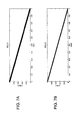
- Figure 2B shows the output intensity using the same four electrodes after the input data has been mapped according to the teachings of the present invention to a pattern of electrode actuation approximating more closely to a linear response.
- electrode actuating device 20 includes a digital-to-digital converter. It will be appreciated that such a converter may be implemented from very straightforward and high-speed logic components which make it feasible to employ the present invention in high frequency systems.
- Electronic input 12 may be simply the input pins of digital-to-digital converter 20.
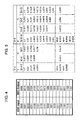
- Figure 4 illustrates a preferred implementation of the digital-to-digital mapping employed to generate the output of Figure 2B .
- a digital-to-digital converter suitable for implementing the various embodiments of the present invention may readily be implemented using commercially available high-speed Application Specific Integrated Circuits ("ASIC"), as will be clear to one ordinarily skilled in the art.
- ASIC Application Specific Integrated Circuits
- One option for further modification of the output is to modify the actuating voltage applied to each electrode, such as by switching between different distinct voltage levels.
- An alternative preferred option for modifying the output to achieve a better approximation to a linear output is modification of the electrode lengths relative to the factor of two series assumed above.
- a non-limiting example of an approach for determining preferred electrode proportions will be presented below in the context of a Mach-Zehnder modulator.
- Figure 2C illustrates the intensity output employing electrodes with lengths in the proportions listed.
- a comparison of the root-mean-square error from linearity for Figures 2B and 2C shows that the adjustment of electrode lengths results in an additional slight improvement to linearity.
- a further option for modifying the performance of modulator device 10 is the addition of one or more additional electrodes, i.e., M>N. This provides an additional degree of freedom for correcting non-linearity of the response.
- each additional electrode is typically half the dimension of the previously smallest electrode.
- the additional electrode dimension is preferably included within an optimization process in order to determine a preferred dimension for the additional electrode(s) along with the other electrodes.
- the electrode lengths are shown for the unmodified series in the first column of Figure 5 and for the optimized length electrodes in the third column of Figure 5 .
- the present invention is described herein in the context of a preferred example of linearization of a modulator device which inherently has a non-linear response, the principles of the present invention may equally be applied to any case where a natural response of a modulator provides a first function and a desired response is a different second function which may be linear or non-linear.
- the present invention may be employed to convert a digital input into an analog output approximating to any desired response curve within the dynamic range of the modulator.
- Non-limiting examples include where a desired output response curve is sinusoidal or exponential, or where it is desired to increase the resolution or "contrast" of the output within a specific range of input values.
- Figures 6A-6C , 7A and 7B illustrate a number of implementations with 8-bit input data words.
- Figure 6A shows the unmodified output of an 8-bit arrangement where each data bit is applied directly to a corresponding electrode, again showing the underlying cosine response of the modulator.
- Figure 6C shows output for a similar device where the electrode lengths have been modified according to the values shown in the fifth column of Figure 5 .
- the device has unmodified electrode lengths as shown in the fourth column of Figure 5
- the electrode lengths are modified according to the proportions shown in the sixth column of Figure 5 .
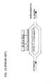
- the Mach-Zehnder modulator is an active integrated waveguide device consisting of a higher index guide region that splits into two paths which are combined again after a certain distance. Each of these paths is referred to as a leg or branch.
- the MZI When used as a switch, the MZI may be turned “off” by raising or lowering the index of refraction in one of the legs. This is achieved by employing the electro-optic effect to produce a 180-degree change in phase by means of optical-path length. Intermediate optical attenuation levels can be obtained by inducing changes other than 180 degrees.
- a 4-bit Digital-to-Analog Converter based on a Multi-Electrode (ME) Mach-Zehnder Interferometer.
- the input to the device consists of 4 bits.
- the Digital-to-Digital converter which may be thought of as a look-up table, the 4 data bits are mapped to 5 electrodes as this realization is equipped with a single excess electrode.
- the optical signal at the output is detected and converted to an electrical (analog) signal.
- the value M is the number of actuating electrodes on each of the two waveguide branches of the modulator.
- T V ⁇ L cos 2 ⁇ 2 ⁇ V ⁇ L T v ⁇ , where the superscript T denotes transposition.
- V j v .
- B i multiplied by v represents the actual (internal) vector of voltages controlling the M electrodes.
- B i should be interpreted as binary vector whose elements are the real numbers ⁇ 0,1 ⁇ .
- V j v
- the lengths of the elements of L and the control vectors B be optimized. As described above, it is possible to optimize one or both of B and L. In practice, optimization of L alone may provide a non-monotonic variation of output together with some improvement in linearity and dynamic range. This may be sufficient for applications in which the non-linearity is relatively small, such as the semiconductor laser embodiments to be discussed below. For more significantly non-linear devices, the options of optimized B with unoptimized L, and optimized B and L are typically more suitable.
- B is optimized, and for any number of electrodes M ; M ⁇ N, it is understood that a binary input data vector D i has to be mapped to a control vector B i , yet B i ⁇ D i .
- the DDC implemented as all-electronic, shall perform this mapping operation.
- RMSE root mean square error
- the optimization problem can now be formulated as minimizing the values of g ( B,L ) for all possible values of the matrix B and the vector L.
- the present invention is not limited to implementations based on Mach-Zehnder modulators, and can be implemented using any device which modulates light intensity as a function of applied voltage.
- Figure 8 shows an analogous implementation of the present invention using an electro-absorption modulator.
- An electro-absorption modulator is a semiconductor device which allows control of the intensity of a laser beam via an electric voltage. Its operational principle is typically based on the Franz-Keldysh effect, i.e., a change of the absorption spectrum caused by an applied electric field, which usually does not involve the excitation of carriers by the electric field.
- this device includes an electronic input 12 for receiving an input data word D of N bits and an electrically controllable modulator 14 with M electrodes for modulating the intensity of an optical signal represented by arrow 16.
- An electrode actuating device 20 is responsive to the input data word D to supply an actuating voltage to the actuating electrodes 18.
- electrode actuating device 20 serves as a Digital-To-Digital Converter is employed to map an N bit input to a set of M electrodes, determining which of the M electrodes is actuated for each input value.
- the particular mapping varies according to the response characteristic of the particular modulator, but the principles of operation are fully analogous to those described above in the context of the Mach-Zehnder modulator implementation.
- the present invention is applicable also to other devices where digital information carried by voltage or current is translated into analog optical signals in the form of optical power.
- LED Light Emitting Diodes
- Figure 9 shows a semiconductor laser implementation of the present invention.
- Figure 9 shows a semiconductor laser DAC device, generally designated 40, constructed and operative according to the teachings of the present invention.
- the actuating electrode typically implemented as a single contiguous electrode, is here subdivided into a threshold electrode 42 and M actuating electrodes 18.
- the threshold electrode 42 is typically needed to reach a minimum activation current below which no significant output is generated.
- Actuating electrodes 18 are actuated as a function of the data bits of a digital input 12, in this case a 4-bit data word, to generate an analog optical signal output of intensity representing the digital input.
- each actuating electrode 18 is part of a set interrelated with effective areas in 2:1 relation, and each electrode is actuated as a function of corresponding single bit of the input data word.
- the actuating current is typically roughly proportional to the area of electrodes actuated. This case is in itself believed to be patentable, and is thought to be of practical importance.
- a closer approximation to a linear response can be achieved by modifying L (electrode proportions) and/or B (by including a DDC, not shown), all according to the principles discussed in detail above.
- threshold electrode 42 may not be necessary. This and any other necessary device-specific modifications will be self-evident to one ordinarily skilled in the art.
- each embodiment of the invention may be modified to provide analog electrical output by use of an optical-to-electrical (O/E) converter.
- O/E optical-to-electrical
- This option is illustrated in Figure 1 as optional O/E converter 30. If the O/E converter itself has a non-linear response function, the present invention may advantageously be used to optimize the system parameters to linearize the electrical output rather than the (intermediate) optical output.
- the present invention is applicable to substantially all applications requiring a DAC with optical or electrical output.
- Examples of particular interest include, but are not limited to, wireless communications systems, fiber-optic communication systems, cellular telephone networks, cable television, military applications, medical applications and hyper/super computer communications.
Landscapes
- Physics & Mathematics (AREA)
- Engineering & Computer Science (AREA)
- Nonlinear Science (AREA)
- Electromagnetism (AREA)
- Computer Networks & Wireless Communication (AREA)
- Signal Processing (AREA)
- Optics & Photonics (AREA)
- General Physics & Mathematics (AREA)
- Theoretical Computer Science (AREA)
- Optical Modulation, Optical Deflection, Nonlinear Optics, Optical Demodulation, Optical Logic Elements (AREA)
- Optical Communication System (AREA)
Applications Claiming Priority (3)
| Application Number | Priority Date | Filing Date | Title |
|---|---|---|---|
| US94355907P | 2007-06-13 | 2007-06-13 | |
| EP08763563.7A EP2174185B1 (de) | 2007-06-13 | 2008-06-12 | System und Verfahren zur Umwandlung digitaler Daten in ein analoges intensitätsmoduliertes optisches Signal |
| PCT/IL2008/000805 WO2008152642A1 (en) | 2007-06-13 | 2008-06-12 | Linearised optical digital modulator |
Related Parent Applications (2)
| Application Number | Title | Priority Date | Filing Date |
|---|---|---|---|
| EP08763563.7A Division EP2174185B1 (de) | 2007-06-13 | 2008-06-12 | System und Verfahren zur Umwandlung digitaler Daten in ein analoges intensitätsmoduliertes optisches Signal |
| EP08763563.7A Division-Into EP2174185B1 (de) | 2007-06-13 | 2008-06-12 | System und Verfahren zur Umwandlung digitaler Daten in ein analoges intensitätsmoduliertes optisches Signal |
Publications (2)
| Publication Number | Publication Date |
|---|---|
| EP2896993A1 true EP2896993A1 (de) | 2015-07-22 |
| EP2896993B1 EP2896993B1 (de) | 2019-04-24 |
Family
ID=39798167
Family Applications (2)
| Application Number | Title | Priority Date | Filing Date |
|---|---|---|---|
| EP08763563.7A Active EP2174185B1 (de) | 2007-06-13 | 2008-06-12 | System und Verfahren zur Umwandlung digitaler Daten in ein analoges intensitätsmoduliertes optisches Signal |
| EP15157901.8A Active EP2896993B1 (de) | 2007-06-13 | 2008-06-12 | System und Verfahren zur Umwandlung digitaler Daten in ein analoges intensitätsmoduliertes optisches Signal |
Family Applications Before (1)
| Application Number | Title | Priority Date | Filing Date |
|---|---|---|---|
| EP08763563.7A Active EP2174185B1 (de) | 2007-06-13 | 2008-06-12 | System und Verfahren zur Umwandlung digitaler Daten in ein analoges intensitätsmoduliertes optisches Signal |
Country Status (3)
| Country | Link |
|---|---|
| US (15) | US8044835B2 (de) |
| EP (2) | EP2174185B1 (de) |
| WO (1) | WO2008152642A1 (de) |
Cited By (1)
| Publication number | Priority date | Publication date | Assignee | Title |
|---|---|---|---|---|
| US9203425B2 (en) | 2007-06-13 | 2015-12-01 | Ramot At Tel-Aviv University Ltd. | Linearized optical digital-to-analog modulator |
Families Citing this family (36)
| Publication number | Priority date | Publication date | Assignee | Title |
|---|---|---|---|---|
| US8320720B2 (en) * | 2009-08-19 | 2012-11-27 | Mark Webster | Advanced modulation formats for silicon-based optical modulators |
| WO2011043079A1 (ja) * | 2009-10-09 | 2011-04-14 | 日本電気株式会社 | 光変調器モジュール及び光信号の変調方法 |
| DE102010048488B4 (de) * | 2010-10-14 | 2013-01-10 | Northrop Grumman Litef Gmbh | Digitaler Modulator |
| US9069193B2 (en) * | 2011-06-01 | 2015-06-30 | Nec Corporation | Optical waveguide device, optical interferometer, and method for producing optical waveguide device |
| WO2013084382A1 (ja) * | 2011-12-06 | 2013-06-13 | 日本電気株式会社 | 光変調器、それを用いた光変調器モジュール、及び光変調信号の補正方法 |
| JP2013120936A (ja) * | 2011-12-07 | 2013-06-17 | Ultratech Inc | パターン効果を低減したGaNLEDのレーザーアニール |
| WO2013121747A1 (ja) * | 2012-02-13 | 2013-08-22 | 日本電気株式会社 | 光変調器および光変調方法 |
| US9459511B2 (en) * | 2012-04-27 | 2016-10-04 | Nec Corporation | Mach-Zehnder type optical modulator, optical transmission/reception system and control method of Mach-Zehnder type optical modulator |
| CN103516610B (zh) * | 2012-06-18 | 2017-12-15 | 华为技术有限公司 | 业务处理方法、设备和系统 |
| JPWO2014141337A1 (ja) * | 2013-03-15 | 2017-02-16 | 日本電気株式会社 | 光変調器、光送信器、光送受信システム及び光変調器の制御方法 |
| US8873896B1 (en) | 2013-05-23 | 2014-10-28 | Jds Uniphase Corporation | Dual polarization optical modulator using dual broadband multi-electrode weighted direct analog phase modulators |
| US9531478B2 (en) * | 2013-11-08 | 2016-12-27 | Futurewei Technologies, Inc. | Digital optical modulator for programmable n-quadrature amplitude modulation generation |
| JP6299337B2 (ja) * | 2014-03-28 | 2018-03-28 | 富士通株式会社 | 位相変調装置及びその制御方法 |
| WO2015161477A1 (zh) * | 2014-04-24 | 2015-10-29 | 华为技术有限公司 | 一种光信号调制通路、电光调制器以及光发射机 |
| US9519162B2 (en) | 2014-10-09 | 2016-12-13 | Coriant Advanced Technology, LLC | Optical modulator having a plurality of modulator segments |
| US20160204868A1 (en) * | 2015-01-13 | 2016-07-14 | Huawei Technologies Co., Ltd. | Summation of Parallel Modulated Signals of Different Wavelengths |
| JP6523060B2 (ja) * | 2015-06-09 | 2019-05-29 | 日本オクラロ株式会社 | 光信号生成装置 |
| JP2017009626A (ja) * | 2015-06-16 | 2017-01-12 | 日本オクラロ株式会社 | 光信号生成装置 |
| US9746698B2 (en) * | 2015-08-21 | 2017-08-29 | Huawei Technologies Co., Ltd. | Electrical crosstalk reduction in a high-order digital optical modulator |
| RU2654383C2 (ru) * | 2015-12-11 | 2018-05-17 | Частное образовательное учреждение высшего образования "ЮЖНЫЙ УНИВЕРСИТЕТ (ИУБиП)" | Оптический цифроаналоговый преобразователь |
| WO2017123243A1 (en) * | 2016-01-15 | 2017-07-20 | Hewlett Packard Enterprise Development Lp | Optical signal modulation |
| US10620375B2 (en) * | 2016-02-09 | 2020-04-14 | Ramot at Tel-Aviv University Ldt. | Modulator using a micro-ring resonator |
| JP6701830B2 (ja) * | 2016-03-11 | 2020-05-27 | 富士通株式会社 | 変調器およびマッハツェンダ型変調器 |
| EP3432058B1 (de) * | 2016-03-18 | 2020-08-05 | Nippon Telegraph And Telephone Corporation | Optischer modulator |
| US10120210B2 (en) | 2016-06-03 | 2018-11-06 | International Business Machines Corporation | Feed-forward optical equalization using an electro-optic modulator with a multi-segment electrode and distributed drivers |
| US10084619B2 (en) | 2016-06-03 | 2018-09-25 | International Business Machines Corporation | Nested feed-forward optical equalization using an electro-optic modulator with a multi-segment electrode |
| US10367586B2 (en) * | 2016-09-01 | 2019-07-30 | Juniper Networks, Inc. | Methods and apparatus for low-loss reconfigurable optical quadrature amplitude modulation (QAM) signal generation |
| JP2018200379A (ja) * | 2017-05-26 | 2018-12-20 | 富士通株式会社 | 光送信器 |
| JP6998691B2 (ja) * | 2017-07-19 | 2022-01-18 | 日本ルメンタム株式会社 | 光送信モジュール |
| WO2020096913A1 (en) | 2018-11-08 | 2020-05-14 | Luminous Computing, Inc. | System and method for photonic computing |
| US11656485B2 (en) * | 2019-07-11 | 2023-05-23 | Luminous Computing, Inc. | Photonic bandgap phase modulator, optical filter bank, photonic computing system, and methods of use |
| RU2744348C1 (ru) * | 2020-04-03 | 2021-03-05 | Федеральное государственное бюджетное образовательное учреждение высшего образования "Ростовский государственный экономический университет (РИНХ)" | Оптический аналого-цифровой преобразователь |
| CN111884727B (zh) * | 2020-07-15 | 2021-11-16 | 杭州电子科技大学 | 一种基于数字映射的高速光子数模转换方法及系统 |
| JP2023088781A (ja) * | 2021-12-15 | 2023-06-27 | 富士通株式会社 | 光送信器 |
| CN116667936A (zh) * | 2022-02-17 | 2023-08-29 | 上海曦智科技有限公司 | 确定引导随机数据采样方法及其系统 |
| WO2024247046A1 (ja) * | 2023-05-29 | 2024-12-05 | 日本電信電話株式会社 | 光変調器 |
Citations (4)
| Publication number | Priority date | Publication date | Assignee | Title |
|---|---|---|---|---|
| US4288785A (en) | 1979-05-23 | 1981-09-08 | Thomson-Csf | Light intensity modulator with digital control and a digital-analog converter comprising such a modulator |
| US5137359A (en) * | 1991-03-18 | 1992-08-11 | Litton Systems, Inc. | Digital phase modulator for fiber optic sagnac interferometer |
| US6781537B1 (en) * | 2003-06-10 | 2004-08-24 | Nortel Networks Limited | High speed digital to analog converter |
| US7061414B2 (en) | 2004-02-03 | 2006-06-13 | Lucent Technologies Inc. | Optical digital-to-analog converter |
Family Cites Families (49)
| Publication number | Priority date | Publication date | Assignee | Title |
|---|---|---|---|---|
| US4613204A (en) | 1983-11-25 | 1986-09-23 | Battelle Memorial Institute | D/A conversion apparatus including electrooptical multipliers |
| US4649505A (en) | 1984-07-02 | 1987-03-10 | General Electric Company | Two-input crosstalk-resistant adaptive noise canceller |
| JPH01226066A (ja) * | 1988-03-04 | 1989-09-08 | Hitachi Ltd | ディジタル信号処理プロセッサ |
| US5010346A (en) * | 1989-10-27 | 1991-04-23 | The Boeing Company | Electro-optical analog-to-digital converter and method for digitizing an analog signal |
| US5521738A (en) * | 1994-06-30 | 1996-05-28 | At&T Corp. | Data encoded optical pulse generator |
| DE69531328T2 (de) | 1994-09-12 | 2004-02-12 | Nippon Telegraph And Telephone Corp. | Intensitätsmoduliertes optisches Übertragungssystem |
| US5625722A (en) * | 1994-12-21 | 1997-04-29 | Lucent Technologies Inc. | Method and apparatus for generating data encoded pulses in return-to-zero format |
| GB2302738B (en) * | 1995-06-28 | 1999-03-03 | Northern Telecom Ltd | Semiconductor modulator with a shift |
| FR2740285B1 (fr) | 1995-10-23 | 1997-11-21 | Alcatel Submarcom | Dispositif de modulation d'amplitude a modulateur a electro-absorption |
| US5917638A (en) | 1997-02-13 | 1999-06-29 | Lucent Technologies, Inc. | Duo-binary signal encoding |
| US5977899A (en) * | 1997-09-25 | 1999-11-02 | Analog Devices, Inc. | Digital-to-analog converter using noise-shaped segmentation |
| DE19753427C1 (de) * | 1997-12-02 | 1999-02-04 | Litef Gmbh | Verfahren und Einrichtung zur Erhöhung der Genauigkeit eines digitalen Phasenmodulators für eine faseroptische Signalübertragungs- oder Meßeinrichtung |
| US6337755B1 (en) * | 1998-11-17 | 2002-01-08 | Qtera Corporation | Polarization independent all-optical regenerators |
| US7013183B1 (en) * | 2000-07-14 | 2006-03-14 | Solvisions Technologies Int'l | Multiplexer hardware and software for control of a deformable mirror |
| JP3721062B2 (ja) | 2000-08-30 | 2005-11-30 | 日本電信電話株式会社 | 光送信機 |
| US7167651B2 (en) * | 2000-09-26 | 2007-01-23 | Celight, Inc. | System and method for code division multiplexed optical communication |
| US6326910B1 (en) * | 2000-11-06 | 2001-12-04 | The United States Of America As Represented By The Secretary Of The Air Force | Photonic analog-to-digital conversion using light absorbers |
| US7173551B2 (en) * | 2000-12-21 | 2007-02-06 | Quellan, Inc. | Increasing data throughput in optical fiber transmission systems |
| US20030076570A1 (en) * | 2001-10-23 | 2003-04-24 | Teradvance Communications, Llc | Method, system and apparatus for optically receiving information |
| JP2003255283A (ja) * | 2002-03-04 | 2003-09-10 | Opnext Japan Inc | マッハツェンダ型光変調器 |
| US7308210B2 (en) * | 2002-04-05 | 2007-12-11 | Kabushiki Kaisha Toshiba | Optical modulating device, optical transmitting apparatus using the same, method of controlling optical modulating device, and control program recording medium |
| US7142788B2 (en) * | 2002-04-16 | 2006-11-28 | Corvis Corporation | Optical communications systems, devices, and methods |
| US7146109B2 (en) * | 2002-04-26 | 2006-12-05 | Lucent Technologies Inc. | Analog modulation of optical signals |
| KR100487224B1 (ko) | 2002-12-18 | 2005-05-03 | 삼성전자주식회사 | 수직공동 표면방사 레이저 및 그 제조방법 |
| DE10307526B4 (de) * | 2003-02-21 | 2005-07-28 | Litef Gmbh | Digitaler Phasenmodulator hoher Auflösung für eine faseroptische Signalübertragungs- oder Messeinrichtung |
| US20040213170A1 (en) * | 2003-04-22 | 2004-10-28 | Gordon Bremer | Extended-performance echo-canceled duplex (EP ECD) communication |
| JP3972066B2 (ja) * | 2004-03-16 | 2007-09-05 | 大日精化工業株式会社 | 光制御式光路切替型データ配信装置および配信方法 |
| US7873284B2 (en) * | 2004-04-22 | 2011-01-18 | Alcatel-Lucent Usa Inc. | Quadrature amplitude modulation of optical carriers |
| US7317845B2 (en) | 2004-06-23 | 2008-01-08 | Lucent Technologies Inc. | Optical modulator having reduced bandwidth requirements and method of operation thereof |
| US7110122B2 (en) * | 2004-07-21 | 2006-09-19 | Hewlett-Packard Development Company, L.P. | Interferometer calibration methods and apparatus |
| GB2419208A (en) * | 2004-10-18 | 2006-04-19 | Qinetiq Ltd | Optical correlation employing an optical bit delay |
| US7403711B2 (en) | 2005-11-22 | 2008-07-22 | Lucent Technologies Inc. | Optical digital-to-analog converter and method of optically converting digital data to analog form |
| US7277603B1 (en) | 2006-02-22 | 2007-10-02 | Nortel Networks Limited | Integrated optical waveform modulation |
| US7564390B2 (en) * | 2006-07-18 | 2009-07-21 | Raytheon Company | Optical digital to analog converter |
| US7978390B2 (en) | 2006-08-30 | 2011-07-12 | Hitachi, Ltd. | Optical modulator |
| US7483597B2 (en) | 2006-10-19 | 2009-01-27 | Lightwire, Inc. | Optical modulator utilizing multi-level signaling |
| JP5092432B2 (ja) | 2007-02-02 | 2012-12-05 | 富士ゼロックス株式会社 | 面発光型半導体レーザ、面発光型半導体レーザの製造方法、光学装置、光照射装置、情報処理装置、光送信装置、光空間伝送装置および光伝送システム |
| US7609935B2 (en) * | 2007-03-23 | 2009-10-27 | Bbn Technologies | Optical vector modulator |
| EP2174185B1 (de) * | 2007-06-13 | 2015-04-22 | Ramot at Tel-Aviv University Ltd. | System und Verfahren zur Umwandlung digitaler Daten in ein analoges intensitätsmoduliertes optisches Signal |
| WO2011010314A2 (en) * | 2009-07-24 | 2011-01-27 | Technion- Research And Development Foundation Ltd. | Ultra-high-speed photonic-enabled adc based on multi-phase interferometry |
| US9331096B2 (en) * | 2009-09-04 | 2016-05-03 | Luxtera, Inc. | Method and system for hybrid integration of optical communication systems |
| JP5665504B2 (ja) | 2010-11-24 | 2015-02-04 | キヤノン株式会社 | 垂直共振器型面発光レーザおよび垂直共振器型面発光レーザアレイ |
| US9490902B2 (en) * | 2015-01-13 | 2016-11-08 | Huawei Technologies Co., Ltd. | Optical power system for digital-to-analog link |
| US20160269121A1 (en) * | 2015-03-09 | 2016-09-15 | Alcatel-Lucent Usa Inc. | Modulator Biasing For Optical Transmission |
| JP6835743B2 (ja) | 2015-06-09 | 2021-02-24 | トランプ フォトニック コンポーネンツ ゲーエムベーハー | 垂直共振器型面発光レーザ |
| US9991966B1 (en) * | 2017-01-06 | 2018-06-05 | Huawei Technologies Canada Co., Ltd. | Optical transmitter |
| KR101818725B1 (ko) | 2017-09-11 | 2018-01-15 | 주식회사 레이아이알 | 수직 공동 표면 방출 레이저 |
| KR102410566B1 (ko) * | 2018-02-05 | 2022-06-17 | 삼성전자주식회사 | 반도체 메모리 장치, 이를 포함하는 메모리 시스템 및 반도체 메모리 장치의 동작 방법 |
| US10389473B1 (en) | 2018-04-27 | 2019-08-20 | Fujitsu Limited | Reach extension for optical networks through control of modulation formats and numbers of subcarriers |
-
2008
- 2008-06-12 EP EP08763563.7A patent/EP2174185B1/de active Active
- 2008-06-12 EP EP15157901.8A patent/EP2896993B1/de active Active
- 2008-06-12 WO PCT/IL2008/000805 patent/WO2008152642A1/en not_active Ceased
-
2009
- 2009-12-14 US US12/636,805 patent/US8044835B2/en active Active
-
2011
- 2011-10-25 US US13/280,371 patent/US8797198B2/en active Active
-
2014
- 2014-07-08 US US14/325,486 patent/US9031417B2/en active Active
-
2015
- 2015-03-19 US US14/662,343 patent/US9203425B2/en active Active
- 2015-10-25 US US14/922,165 patent/US9479191B2/en active Active
-
2016
- 2016-10-20 US US15/298,373 patent/US10205527B2/en active Active
- 2016-10-20 US US15/298,327 patent/US10033465B2/en active Active
-
2018
- 2018-12-28 US US16/234,635 patent/US10270535B1/en active Active
-
2019
- 2019-04-17 US US16/386,391 patent/US10461866B2/en active Active
- 2019-08-06 US US16/532,567 patent/US11133872B2/en active Active
-
2021
- 2021-09-22 US US17/481,904 patent/US11342998B2/en active Active
-
2022
- 2022-05-04 US US17/736,876 patent/US11716148B2/en active Active
-
2023
- 2023-06-13 US US18/334,269 patent/US12191912B2/en active Active
-
2024
- 2024-09-03 US US18/822,532 patent/US12388533B2/en active Active
-
2025
- 2025-07-21 US US19/274,676 patent/US20250350366A1/en active Pending
Patent Citations (4)
| Publication number | Priority date | Publication date | Assignee | Title |
|---|---|---|---|---|
| US4288785A (en) | 1979-05-23 | 1981-09-08 | Thomson-Csf | Light intensity modulator with digital control and a digital-analog converter comprising such a modulator |
| US5137359A (en) * | 1991-03-18 | 1992-08-11 | Litton Systems, Inc. | Digital phase modulator for fiber optic sagnac interferometer |
| US6781537B1 (en) * | 2003-06-10 | 2004-08-24 | Nortel Networks Limited | High speed digital to analog converter |
| US7061414B2 (en) | 2004-02-03 | 2006-06-13 | Lucent Technologies Inc. | Optical digital-to-analog converter |
Non-Patent Citations (2)
| Title |
|---|
| LEVEN: "A 12.5 gsamples/s optical digital-to-analog converter with 3.8 effective bits", LASERS AND ELECTRO-OPTICS SOCIETY, 2004. LEOS 2004. THE 17TH ANNUAL MEETING OF THE IEEE, vol. 1, November 2004 (2004-11-01), pages 270 - 271 |
| YACOUBIAN: "Digital-to-analog conversion using electrooptic modulators", IEEE PHOTONICS TECHNOLOGY LETTERS, vol. 15, January 2003 (2003-01-01), pages 117 - 119 |
Cited By (11)
| Publication number | Priority date | Publication date | Assignee | Title |
|---|---|---|---|---|
| US9203425B2 (en) | 2007-06-13 | 2015-12-01 | Ramot At Tel-Aviv University Ltd. | Linearized optical digital-to-analog modulator |
| US9479191B2 (en) | 2007-06-13 | 2016-10-25 | Ramot At Tel-Aviv University Ltd. | Linearized optical digital-to-analog modulator |
| US10033465B2 (en) | 2007-06-13 | 2018-07-24 | Ramot At Tel-Aviv University Ltd. | Linearized optical digital-to-analog modulator |
| US10205527B2 (en) | 2007-06-13 | 2019-02-12 | Ramot At Tel-Aviv University Ltd. | Linearized optical digital-to-analog modulator |
| US10270535B1 (en) | 2007-06-13 | 2019-04-23 | Ramot At Tel-Aviv University Ltd. | Linearized optical digital-to-analog modulator |
| US10461866B2 (en) | 2007-06-13 | 2019-10-29 | Ramot At Tel-Aviv University Ltd. | Linearized optical digital-to-analog modulator |
| US11133872B2 (en) | 2007-06-13 | 2021-09-28 | Ramot At Tel-Aviv University Ltd. | Linearized optical digital-to-analog modulator |
| US11342998B2 (en) | 2007-06-13 | 2022-05-24 | Ramot At Tel-Aviv University Ltd. | Linearized optical digital-to-analog modulator |
| US11716148B2 (en) | 2007-06-13 | 2023-08-01 | Ramot At Tel Aviv University Ltd. | Linearized optical digital-to-analog modulator |
| US12191912B2 (en) | 2007-06-13 | 2025-01-07 | Ramot At Tel-Aviv University Ltd. | Linearized optical digital-to-analog modulator |
| US12388533B2 (en) | 2007-06-13 | 2025-08-12 | Ramot At Tel-Aviv University Ltd. | Linearized optical digital-to-analog modulator |
Also Published As
| Publication number | Publication date |
|---|---|
| US20170294968A1 (en) | 2017-10-12 |
| US11133872B2 (en) | 2021-09-28 |
| US8797198B2 (en) | 2014-08-05 |
| US20250350366A1 (en) | 2025-11-13 |
| US20220077936A1 (en) | 2022-03-10 |
| US10205527B2 (en) | 2019-02-12 |
| US12191912B2 (en) | 2025-01-07 |
| US9203425B2 (en) | 2015-12-01 |
| WO2008152642A1 (en) | 2008-12-18 |
| US20170302291A1 (en) | 2017-10-19 |
| US20230403079A1 (en) | 2023-12-14 |
| US11342998B2 (en) | 2022-05-24 |
| US11716148B2 (en) | 2023-08-01 |
| EP2174185A1 (de) | 2010-04-14 |
| US10461866B2 (en) | 2019-10-29 |
| EP2896993B1 (de) | 2019-04-24 |
| US20160043732A1 (en) | 2016-02-11 |
| US20240430011A1 (en) | 2024-12-26 |
| US8044835B2 (en) | 2011-10-25 |
| US20120081245A1 (en) | 2012-04-05 |
| US10270535B1 (en) | 2019-04-23 |
| US20190273561A1 (en) | 2019-09-05 |
| US20220271842A1 (en) | 2022-08-25 |
| US20190363798A1 (en) | 2019-11-28 |
| US12388533B2 (en) | 2025-08-12 |
| US9479191B2 (en) | 2016-10-25 |
| US9031417B2 (en) | 2015-05-12 |
| US20140321857A1 (en) | 2014-10-30 |
| EP2174185B1 (de) | 2015-04-22 |
| US20100156679A1 (en) | 2010-06-24 |
| US20150194982A1 (en) | 2015-07-09 |
| US10033465B2 (en) | 2018-07-24 |
Similar Documents
| Publication | Publication Date | Title |
|---|---|---|
| EP2896993B1 (de) | System und Verfahren zur Umwandlung digitaler Daten in ein analoges intensitätsmoduliertes optisches Signal | |
| CN102282784B (zh) | 光发送器 | |
| US9977310B2 (en) | Multi-electrode photonic digital to analog converting vector modulator | |
| US11294123B2 (en) | Modulator using a micro-ring resonator | |
| EP3326026B1 (de) | Dämpfung von elektrischem übersprechen bei einem digitalen modulator höherer optischer | |
| Ehrlichman et al. | Improved digital-to-analog conversion using multi-electrode Mach–Zehnder interferometer | |
| KR101542757B1 (ko) | 디지털 신호를 광 펄스들로 변환하기 위한 방법 | |
| Leven et al. | A 12.5 Gsample/s optical digital-to-analog converter with 3.8 effective bits | |
| US20170054509A1 (en) | Digital-to-Analog Optical Modulator Electrical Crosstalk Reduction | |
| Ehrlichman et al. | Photonic Digital to Analog conversion | |
| Zhang et al. | Design on serial optical digital-to-analog converter and its experiment |
Legal Events
| Date | Code | Title | Description |
|---|---|---|---|
| PUAI | Public reference made under article 153(3) epc to a published international application that has entered the european phase |
Free format text: ORIGINAL CODE: 0009012 |
|
| 17P | Request for examination filed |
Effective date: 20150305 |
|
| AC | Divisional application: reference to earlier application |
Ref document number: 2174185 Country of ref document: EP Kind code of ref document: P |
|
| AK | Designated contracting states |
Kind code of ref document: A1 Designated state(s): AT BE BG CH CY CZ DE DK EE ES FI FR GB GR HR HU IE IS IT LI LT LU LV MC MT NL NO PL PT RO SE SI SK TR |
|
| 17P | Request for examination filed |
Effective date: 20160121 |
|
| RBV | Designated contracting states (corrected) |
Designated state(s): AT BE BG CH CY CZ DE DK EE ES FI FR GB GR HR HU IE IS IT LI LT LU LV MC MT NL NO PL PT RO SE SI SK TR |
|
| STAA | Information on the status of an ep patent application or granted ep patent |
Free format text: STATUS: EXAMINATION IS IN PROGRESS |
|
| 17Q | First examination report despatched |
Effective date: 20170802 |
|
| REG | Reference to a national code |
Ref country code: DE Ref legal event code: R079 Ref document number: 602008059884 Country of ref document: DE Free format text: PREVIOUS MAIN CLASS: G02F0007000000 Ipc: G02F0001015000 |
|
| RIC1 | Information provided on ipc code assigned before grant |
Ipc: H03M 1/00 20060101ALN20190115BHEP Ipc: H04B 10/25 20130101ALN20190115BHEP Ipc: G02F 1/225 20060101ALI20190115BHEP Ipc: G02F 1/015 20060101AFI20190115BHEP Ipc: G02F 7/00 20060101ALN20190115BHEP Ipc: H04B 10/54 20130101ALN20190115BHEP Ipc: G02F 1/21 20060101ALI20190115BHEP Ipc: H03M 1/70 20060101ALN20190115BHEP Ipc: H04B 10/50 20130101ALN20190115BHEP Ipc: G02F 1/01 20060101ALI20190115BHEP |
|
| GRAP | Despatch of communication of intention to grant a patent |
Free format text: ORIGINAL CODE: EPIDOSNIGR1 |
|
| STAA | Information on the status of an ep patent application or granted ep patent |
Free format text: STATUS: GRANT OF PATENT IS INTENDED |
|
| RIC1 | Information provided on ipc code assigned before grant |
Ipc: H03M 1/70 20060101ALN20190206BHEP Ipc: H04B 10/50 20130101ALN20190206BHEP Ipc: H04B 10/54 20130101ALN20190206BHEP Ipc: G02F 1/015 20060101AFI20190206BHEP Ipc: G02F 1/01 20060101ALI20190206BHEP Ipc: H03M 1/00 20060101ALN20190206BHEP Ipc: G02F 7/00 20060101ALN20190206BHEP Ipc: G02F 1/225 20060101ALI20190206BHEP Ipc: H04B 10/25 20130101ALN20190206BHEP Ipc: G02F 1/21 20060101ALI20190206BHEP |
|
| GRAS | Grant fee paid |
Free format text: ORIGINAL CODE: EPIDOSNIGR3 |
|
| GRAA | (expected) grant |
Free format text: ORIGINAL CODE: 0009210 |
|
| STAA | Information on the status of an ep patent application or granted ep patent |
Free format text: STATUS: THE PATENT HAS BEEN GRANTED |
|
| INTG | Intention to grant announced |
Effective date: 20190304 |
|
| AC | Divisional application: reference to earlier application |
Ref document number: 2174185 Country of ref document: EP Kind code of ref document: P |
|
| AK | Designated contracting states |
Kind code of ref document: B1 Designated state(s): AT BE BG CH CY CZ DE DK EE ES FI FR GB GR HR HU IE IS IT LI LT LU LV MC MT NL NO PL PT RO SE SI SK TR |
|
| REG | Reference to a national code |
Ref country code: GB Ref legal event code: FG4D |
|
| REG | Reference to a national code |
Ref country code: CH Ref legal event code: EP |
|
| REG | Reference to a national code |
Ref country code: AT Ref legal event code: REF Ref document number: 1124816 Country of ref document: AT Kind code of ref document: T Effective date: 20190515 Ref country code: IE Ref legal event code: FG4D |
|
| REG | Reference to a national code |
Ref country code: DE Ref legal event code: R096 Ref document number: 602008059884 Country of ref document: DE |
|
| REG | Reference to a national code |
Ref country code: NL Ref legal event code: MP Effective date: 20190424 |
|
| REG | Reference to a national code |
Ref country code: LT Ref legal event code: MG4D |
|
| PG25 | Lapsed in a contracting state [announced via postgrant information from national office to epo] |
Ref country code: NL Free format text: LAPSE BECAUSE OF FAILURE TO SUBMIT A TRANSLATION OF THE DESCRIPTION OR TO PAY THE FEE WITHIN THE PRESCRIBED TIME-LIMIT Effective date: 20190424 |
|
| PG25 | Lapsed in a contracting state [announced via postgrant information from national office to epo] |
Ref country code: FI Free format text: LAPSE BECAUSE OF FAILURE TO SUBMIT A TRANSLATION OF THE DESCRIPTION OR TO PAY THE FEE WITHIN THE PRESCRIBED TIME-LIMIT Effective date: 20190424 Ref country code: LT Free format text: LAPSE BECAUSE OF FAILURE TO SUBMIT A TRANSLATION OF THE DESCRIPTION OR TO PAY THE FEE WITHIN THE PRESCRIBED TIME-LIMIT Effective date: 20190424 Ref country code: SE Free format text: LAPSE BECAUSE OF FAILURE TO SUBMIT A TRANSLATION OF THE DESCRIPTION OR TO PAY THE FEE WITHIN THE PRESCRIBED TIME-LIMIT Effective date: 20190424 Ref country code: NO Free format text: LAPSE BECAUSE OF FAILURE TO SUBMIT A TRANSLATION OF THE DESCRIPTION OR TO PAY THE FEE WITHIN THE PRESCRIBED TIME-LIMIT Effective date: 20190724 Ref country code: PT Free format text: LAPSE BECAUSE OF FAILURE TO SUBMIT A TRANSLATION OF THE DESCRIPTION OR TO PAY THE FEE WITHIN THE PRESCRIBED TIME-LIMIT Effective date: 20190824 Ref country code: HR Free format text: LAPSE BECAUSE OF FAILURE TO SUBMIT A TRANSLATION OF THE DESCRIPTION OR TO PAY THE FEE WITHIN THE PRESCRIBED TIME-LIMIT Effective date: 20190424 Ref country code: ES Free format text: LAPSE BECAUSE OF FAILURE TO SUBMIT A TRANSLATION OF THE DESCRIPTION OR TO PAY THE FEE WITHIN THE PRESCRIBED TIME-LIMIT Effective date: 20190424 |
|
| PG25 | Lapsed in a contracting state [announced via postgrant information from national office to epo] |
Ref country code: GR Free format text: LAPSE BECAUSE OF FAILURE TO SUBMIT A TRANSLATION OF THE DESCRIPTION OR TO PAY THE FEE WITHIN THE PRESCRIBED TIME-LIMIT Effective date: 20190725 Ref country code: BG Free format text: LAPSE BECAUSE OF FAILURE TO SUBMIT A TRANSLATION OF THE DESCRIPTION OR TO PAY THE FEE WITHIN THE PRESCRIBED TIME-LIMIT Effective date: 20190724 Ref country code: LV Free format text: LAPSE BECAUSE OF FAILURE TO SUBMIT A TRANSLATION OF THE DESCRIPTION OR TO PAY THE FEE WITHIN THE PRESCRIBED TIME-LIMIT Effective date: 20190424 Ref country code: PL Free format text: LAPSE BECAUSE OF FAILURE TO SUBMIT A TRANSLATION OF THE DESCRIPTION OR TO PAY THE FEE WITHIN THE PRESCRIBED TIME-LIMIT Effective date: 20190424 |
|
| REG | Reference to a national code |
Ref country code: AT Ref legal event code: MK05 Ref document number: 1124816 Country of ref document: AT Kind code of ref document: T Effective date: 20190424 |
|
| PG25 | Lapsed in a contracting state [announced via postgrant information from national office to epo] |
Ref country code: IS Free format text: LAPSE BECAUSE OF FAILURE TO SUBMIT A TRANSLATION OF THE DESCRIPTION OR TO PAY THE FEE WITHIN THE PRESCRIBED TIME-LIMIT Effective date: 20190824 |
|
| REG | Reference to a national code |
Ref country code: DE Ref legal event code: R097 Ref document number: 602008059884 Country of ref document: DE |
|
| PG25 | Lapsed in a contracting state [announced via postgrant information from national office to epo] |
Ref country code: EE Free format text: LAPSE BECAUSE OF FAILURE TO SUBMIT A TRANSLATION OF THE DESCRIPTION OR TO PAY THE FEE WITHIN THE PRESCRIBED TIME-LIMIT Effective date: 20190424 Ref country code: DK Free format text: LAPSE BECAUSE OF FAILURE TO SUBMIT A TRANSLATION OF THE DESCRIPTION OR TO PAY THE FEE WITHIN THE PRESCRIBED TIME-LIMIT Effective date: 20190424 Ref country code: SK Free format text: LAPSE BECAUSE OF FAILURE TO SUBMIT A TRANSLATION OF THE DESCRIPTION OR TO PAY THE FEE WITHIN THE PRESCRIBED TIME-LIMIT Effective date: 20190424 Ref country code: MC Free format text: LAPSE BECAUSE OF FAILURE TO SUBMIT A TRANSLATION OF THE DESCRIPTION OR TO PAY THE FEE WITHIN THE PRESCRIBED TIME-LIMIT Effective date: 20190424 Ref country code: AT Free format text: LAPSE BECAUSE OF FAILURE TO SUBMIT A TRANSLATION OF THE DESCRIPTION OR TO PAY THE FEE WITHIN THE PRESCRIBED TIME-LIMIT Effective date: 20190424 Ref country code: RO Free format text: LAPSE BECAUSE OF FAILURE TO SUBMIT A TRANSLATION OF THE DESCRIPTION OR TO PAY THE FEE WITHIN THE PRESCRIBED TIME-LIMIT Effective date: 20190424 Ref country code: CZ Free format text: LAPSE BECAUSE OF FAILURE TO SUBMIT A TRANSLATION OF THE DESCRIPTION OR TO PAY THE FEE WITHIN THE PRESCRIBED TIME-LIMIT Effective date: 20190424 |
|
| REG | Reference to a national code |
Ref country code: CH Ref legal event code: PL |
|
| PG25 | Lapsed in a contracting state [announced via postgrant information from national office to epo] |
Ref country code: IT Free format text: LAPSE BECAUSE OF FAILURE TO SUBMIT A TRANSLATION OF THE DESCRIPTION OR TO PAY THE FEE WITHIN THE PRESCRIBED TIME-LIMIT Effective date: 20190424 |
|
| PLBE | No opposition filed within time limit |
Free format text: ORIGINAL CODE: 0009261 |
|
| STAA | Information on the status of an ep patent application or granted ep patent |
Free format text: STATUS: NO OPPOSITION FILED WITHIN TIME LIMIT |
|
| REG | Reference to a national code |
Ref country code: BE Ref legal event code: MM Effective date: 20190630 |
|
| PG25 | Lapsed in a contracting state [announced via postgrant information from national office to epo] |
Ref country code: TR Free format text: LAPSE BECAUSE OF FAILURE TO SUBMIT A TRANSLATION OF THE DESCRIPTION OR TO PAY THE FEE WITHIN THE PRESCRIBED TIME-LIMIT Effective date: 20190424 |
|
| 26N | No opposition filed |
Effective date: 20200127 |
|
| PG25 | Lapsed in a contracting state [announced via postgrant information from national office to epo] |
Ref country code: IE Free format text: LAPSE BECAUSE OF NON-PAYMENT OF DUE FEES Effective date: 20190612 |
|
| PG25 | Lapsed in a contracting state [announced via postgrant information from national office to epo] |
Ref country code: LI Free format text: LAPSE BECAUSE OF NON-PAYMENT OF DUE FEES Effective date: 20190630 Ref country code: BE Free format text: LAPSE BECAUSE OF NON-PAYMENT OF DUE FEES Effective date: 20190630 Ref country code: SI Free format text: LAPSE BECAUSE OF FAILURE TO SUBMIT A TRANSLATION OF THE DESCRIPTION OR TO PAY THE FEE WITHIN THE PRESCRIBED TIME-LIMIT Effective date: 20190424 Ref country code: CH Free format text: LAPSE BECAUSE OF NON-PAYMENT OF DUE FEES Effective date: 20190630 Ref country code: LU Free format text: LAPSE BECAUSE OF NON-PAYMENT OF DUE FEES Effective date: 20190612 |
|
| PG25 | Lapsed in a contracting state [announced via postgrant information from national office to epo] |
Ref country code: CY Free format text: LAPSE BECAUSE OF FAILURE TO SUBMIT A TRANSLATION OF THE DESCRIPTION OR TO PAY THE FEE WITHIN THE PRESCRIBED TIME-LIMIT Effective date: 20190424 |
|
| PG25 | Lapsed in a contracting state [announced via postgrant information from national office to epo] |
Ref country code: HU Free format text: LAPSE BECAUSE OF FAILURE TO SUBMIT A TRANSLATION OF THE DESCRIPTION OR TO PAY THE FEE WITHIN THE PRESCRIBED TIME-LIMIT; INVALID AB INITIO Effective date: 20080612 Ref country code: MT Free format text: LAPSE BECAUSE OF FAILURE TO SUBMIT A TRANSLATION OF THE DESCRIPTION OR TO PAY THE FEE WITHIN THE PRESCRIBED TIME-LIMIT Effective date: 20190424 |
|
| P01 | Opt-out of the competence of the unified patent court (upc) registered |
Effective date: 20230526 |
|
| PGFP | Annual fee paid to national office [announced via postgrant information from national office to epo] |
Ref country code: DE Payment date: 20250618 Year of fee payment: 18 |
|
| PGFP | Annual fee paid to national office [announced via postgrant information from national office to epo] |
Ref country code: GB Payment date: 20250618 Year of fee payment: 18 |
|
| PGFP | Annual fee paid to national office [announced via postgrant information from national office to epo] |
Ref country code: FR Payment date: 20250625 Year of fee payment: 18 |