EP2897293A1 - Convertisseur numérique/analogique et procédé d'étalonnage d'un convertisseur numérique/analogique - Google Patents
Convertisseur numérique/analogique et procédé d'étalonnage d'un convertisseur numérique/analogique Download PDFInfo
- Publication number
- EP2897293A1 EP2897293A1 EP15151291.0A EP15151291A EP2897293A1 EP 2897293 A1 EP2897293 A1 EP 2897293A1 EP 15151291 A EP15151291 A EP 15151291A EP 2897293 A1 EP2897293 A1 EP 2897293A1
- Authority
- EP
- European Patent Office
- Prior art keywords
- msb
- combination
- lsb
- electrical
- field
- Prior art date
- Legal status (The legal status is an assumption and is not a legal conclusion. Google has not performed a legal analysis and makes no representation as to the accuracy of the status listed.)
- Withdrawn
Links
Images


Classifications
-
- H—ELECTRICITY
- H03—ELECTRONIC CIRCUITRY
- H03M—CODING; DECODING; CODE CONVERSION IN GENERAL
- H03M1/00—Analogue/digital conversion; Digital/analogue conversion
- H03M1/10—Calibration or testing
- H03M1/1009—Calibration
- H03M1/1033—Calibration over the full range of the converter, e.g. for correcting differential non-linearity
-
- H—ELECTRICITY
- H03—ELECTRONIC CIRCUITRY
- H03M—CODING; DECODING; CODE CONVERSION IN GENERAL
- H03M1/00—Analogue/digital conversion; Digital/analogue conversion
- H03M1/06—Continuously compensating for, or preventing, undesired influence of physical parameters
- H03M1/0617—Continuously compensating for, or preventing, undesired influence of physical parameters characterised by the use of methods or means not specific to a particular type of detrimental influence
- H03M1/0675—Continuously compensating for, or preventing, undesired influence of physical parameters characterised by the use of methods or means not specific to a particular type of detrimental influence using redundancy
- H03M1/069—Continuously compensating for, or preventing, undesired influence of physical parameters characterised by the use of methods or means not specific to a particular type of detrimental influence using redundancy by range overlap between successive stages or steps
-
- H—ELECTRICITY
- H03—ELECTRONIC CIRCUITRY
- H03M—CODING; DECODING; CODE CONVERSION IN GENERAL
- H03M1/00—Analogue/digital conversion; Digital/analogue conversion
- H03M1/12—Analogue/digital converters
- H03M1/34—Analogue value compared with reference values
- H03M1/38—Analogue value compared with reference values sequentially only, e.g. successive approximation type
- H03M1/46—Analogue value compared with reference values sequentially only, e.g. successive approximation type with digital/analogue converter for supplying reference values to converter
- H03M1/466—Analogue value compared with reference values sequentially only, e.g. successive approximation type with digital/analogue converter for supplying reference values to converter using switched capacitors
- H03M1/468—Analogue value compared with reference values sequentially only, e.g. successive approximation type with digital/analogue converter for supplying reference values to converter using switched capacitors in which the input S/H circuit is merged with the feedback DAC array
-
- H—ELECTRICITY
- H03—ELECTRONIC CIRCUITRY
- H03M—CODING; DECODING; CODE CONVERSION IN GENERAL
- H03M1/00—Analogue/digital conversion; Digital/analogue conversion
- H03M1/66—Digital/analogue converters
- H03M1/68—Digital/analogue converters with conversions of different sensitivity, i.e. one conversion relating to the more significant digital bits and another conversion to the less significant bits
Definitions
- Embodiments of the present invention relate to a digital-to-analog converter, an analog-to-digital converter with a digital-to-analog converter, and to a calibration method for calibrating a digital-to-analog converter.
- Analog-to-digital converters serve to convert an analog input signal (hereinafter referred to as measurement signal) into digital data, e.g. into a bitstream, to convert.
- the measurement signal is time-quantized in order to subdivide it into individual samples and to sample the individual samples in relation to their value, such that a digital value, e.g. a binary value with a resolution (specified in bits) can be assigned.
- the temporal quantization can be realized, for example, by a sample-and-hold circuit, whereby there are different approaches for value-based quantization.
- Successive-approximation analog-to-digital converters work on the principle of interval interleaving.
- a measurement signal is compared with a reference value generated by a digital-to-analog converter (DAC).
- DAC digital-to-analog converter
- DAC digital-to-analog converter
- a new reference value is generated and the method is repeated accordingly.
- the process is iterated until a change in the reference value leads to an unresolvable change in the comparison and / or the DA converter has reached its finest level. In this case, it is advantageous if, during generation of the reference signal, the change steps decrease with increasing iteration.
- the smallest level of change represented by the Least Significant Bit (LSB) defines the resolution capability of the sample; In this case, however, the dynamic range is to be considered, which is formed as a quotient of the largest and the smallest representable value.
- the accuracy and linearity of the conversion method in the analog-to-digital conversion depend very much on the linearity of the digital-to-analog converter used. In this respect, increasing the precession in DA conversion improves precession in AD conversion.
- the basic capacities that are used for the digital-to-analog converter can be chosen so large that the manufacturing variations have no influence.
- the background to this is that the relative variations in most integrated devices decrease with the root of the surface. This leads to an increased space requirement and thus also to increased power consumption of the entire system.
- an analog calibration can be performed.
- An additional calibration DAC is used, which compensates for variations in the main DAC.
- the required calibration values are measured after production with an exact signal source. In this case, however, additional analog circuit technology is needed.
- a correction of the digital output value can take place subsequently by means of a so-called digital calibration.
- the individual capacities are measured in advance in order to derive a correction value.
- the determination of the correction value is possible for example by measuring the analog-to-digital converter with the aid of an exact signal source.
- Um et al. entitled “A Digital-Domain Calibration of Split-Capacitor DAC for a Differential SAR ADC without Additional Analogue Circuits” describes self-calibration through reconfiguration of the analog to digital converter. Such a self-calibration is also possible by an additional analog circuit, as in the patent US 4970514 is described.
- the methods and circuits shown here frequently entail the disadvantages of analog circuit technology or that very exact correction values for the specific circuit must be determined. Therefore, there is a need for an improved approach.
- the object of the present invention is to provide a concept for a digital to analogue converter, e.g. For use in an analog-to-digital converter to provide with Diskalibri für strength, which is characterized in particular by high precision and ease of use and universal use.
- Embodiments of the present invention provide a digital-to-analog converter having an MSB field, an LSB field, a coupling element, and a calibration unit.
- the Most Significant Bit (MSB) field that is, the field containing the electrical circuit element comprising the Most Significant Bit (MSB), comprises a plurality of electrical components form a common MSB summation point, and each selectively acted upon in accordance with a MSB combination by means of an electrical switching element on.
- the LSB (Least Significant Bit Field) field that is to say the field which comprises the electrical component associated with the least significant bit (LSB), has a second plurality of the electrical components which form a common LSB summation point and each acted upon in accordance with an LSB combination by means of the electrical switching signal on.
- the coupling element couples the LSB summing point and the MSB summing point to each other.
- the electrical components of the MSB field and the LSB field (when the electrical switching signal is applied) produce an electrical signal at the summing point which is coupled to the MSB summing point and the LSB summing point or which may be the MSB summation point.
- the calibration unit is designed to determine the respective tolerance values for the electrical components of the MSB field. For this purpose, with the aid of or consideration of a first LSB combination, a first electrical signal, which is established as a result of the first MSB combination, is determined at the summation point. In a next step, the first MSB combination is varied to obtain a second MSB combination.
- the MSB combination can be varied, for example, by a tolerance-afflicted least bit value for the MSB field (ie, for example, in one step), which means, for example, +/- 15%, +/- 5% or +/- 1%.
- a second LSB combination is determined, which leads to an electrical signal (together with the second MSB combination) at the summing point, the second electrical signal being comparable to the first electrical signal ie leads to the same (analog) electrical signal or, to be exact, in a tolerance range of, for example, +/- 15% equal to the first electrical signal).
- a first tolerance value for an electrical component of the MSB field eg for the lowest bit weighted electrical component
- information about a further tolerance value for a group of electrical components of the MSB field which typically at least the electrical component associated with the least significant bits and the electrical component associated with the next larger bit significance.
- the core of the present invention is thus that the digital-to-analog converter with an MSB field and an LSB field or at least the result-significant components, ie the MSB components (components with the higher bit weight, MSB field) of the digital-to-analog converter, can be measured by means of a special algorithm with the aid of the LSB field.
- two redundant combinations are sought (each consisting of an MSB combination and possibly an LSB combination), which lead to the same, adjusting analog output signal of the DA converter.
- a first of the two redundant binary combinations may be based on a predetermined MSB combination e.g.
- a typical SAR algorithm that is to say by varying the LSB combination, while the second one after variations of the MSB combination, preferably by a low value (eg by a lowest bit value of the MSB field), likewise under variation of the LSB Combination (with the SAR algorithm) is determined.
- the second selected MSB combination is selected one of which is typically known that for these a redundant combination, ie in particular a suitable LSB combination can give. This requirement is typically fulfilled when the change in the MSB field relative to the absolute value is not too great or, in concrete terms, does not exceed the influence of the LSB field on the resulting electrical signal at the output.
- the electrical components eg, the capacitances
- the electrical components of the LSB field and of the MSB field are equal or approximately equal in terms of their number and in particular with regard to their dimensioning.
- the coupling element for coupling the LSB field and the MSB field, ie, if the coupling element, for example a coupling capacitor, is designed accordingly, without further facilities Only by skillful control and by successive approximation by means of the LSB field by means of an MSB combination and an LSB combination, the tolerances of the electrical components in the MSB field can be determined.
- the complement is typically chosen such that for each value MSB1 and MSB2 there is at least one value LSB1 and LSB2 which produces the same voltage at the output of the DA converter.
- the tolerance values always refer to a component which can be assigned to the lowest bit significance in the MSB field or to a combination of electrical components comprising at least the lowest bit value electrical component and an electrical component having a next higher bit significance.
- a system of equations can be established by solving which specific tolerance values for the individual electrical components of the MSB field can be determined.
- the digital-to-analog converter described herein may be combined with a comparator to form an analog-to-digital converter.
- this analog-to-digital converter may further comprise a post-processing unit which is designed to post-process or correct the result of the digitization on the basis of the selective tolerance values or generally on the basis of the determined tolerance values.
- the analog measurement signal to be determined by means of the AD converter via the electrical components realized by way of example as capacitances, so that a sample-and-hold circuit is realized by the DA converter at the same time, since the measurement signal to be sampled is based on the capacitances of the MSB field or the LSB field can be stored.
- the method comprises the basic steps of determining the first electrical signal at the summation point with the aid of a first MSB combination and varying the first MSB combination; a second MSB combination is determined using a second MSB combination, which together with the second MSB combination MSB combination results in a second electrical signal at the summing point, which is similar to the first electrical signal apart from a metrological tolerance.
- a first tolerance value for an electrical component of the MSB field (component with the lowest bit value) or a further tolerance value for a group of electrical components of the MSB field can be determined on the basis of the first and second LSB combination.
- a difference between the first and the second LSB combination is taken when determining the tolerance values.
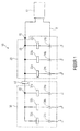
- Fig. 1 shows a digital-to-analog converter 10 with a calibration unit 12.
- the digital-analog converter 10 comprises an MSB field 20 and an LSB field 30.
- Both the MSB field 20 and the LSB field 30 each include a plurality on electrical components 22a-22c for the MSB field 20 and 32a-32c for the LSB field 30.
- the electrical components may be, for example resistors (R) or capacitances (C) and on the one hand with a common summation point (see MSB summing junction 26 and LSB summing junction 36) and each configured to be switchably coupled to switching signal source V REF + such that an electrical switching signal may be applied between summing junction 26 and 36, respectively (compare V REF + ).
- the selective switching capability can be realized by virtue of the fact that a respective switch 24a-24c or, respectively, is provided for each of the electrical components 22a-22c or 32a-32c. 34a-34c is provided between the respective electrical component 22a-22c or 32a-32c and the electrical switching signal source (compare V REF + ).
- the two fields 20 and 30 are coupled to each other via a common coupling element 14.
- the coupling element 14 which may for example also comprise a capacitance or a resistor, connects the two summing points 26 and 36 to each other, so that, for example, through the summing point 26 of the MSB field, a common summation point 16 for the entire digital-to-analog converter 10 is formed or so that the two summing points 26 and 36 are connected to the common summing point 16.
- the calibration unit 12 is at least informally coupled to this common summing point 16 and (at least in the calibration mode) designed to switch the electrical components 22a-22c and 32a-32c here via the switches 24a-24c and 34a-34c.
- This situation is illustrated by the second information coupling (see signal line 18).
- this signal line 18 can be realized either by direct networking with the switches 24a-24c and 34a-34c or by an informational coupling to a control unit (not shown) for driving the switches 24a-24c or 34a-34c ,
- the two fields 20 and 30 are realized as capacity fields, which are coupled to one another via the coupling element 14 or the coupling capacitor 14.
- the conductance values or capacitance values can be designed, for example, as a binary sequence (binary staggering), ie, the capacitances 22a-22c and the capacitances 32a-32c are weighted binary to one another. This binary weighting can for example be attributed to a unit capacity C UNIT .
- the capacity 22c corresponds to the unit capacity C UNIT or the smallest capacity in the MSB field 20 C 0 .
- the next larger capacity 22b or C 1 is typically designed twice as large, so 2 x C UNIT .
- the subsequent capacitance 22a or C 2 is again doubled in terms of their size, ie 2 ⁇ 2 ⁇ C UNIT .
- the coupling capacitance 14 or C KOPPEL typically a ( conductance ) or capacitance value is selected which is at least as large as the unit capacity C UNIT , preferably even greater.
- the binary staggering of the capacities from 22a to 22c in the second capacitance field 30 can be achieved.
- the background to this is that, for example, viewed from the summation point 16 of the circuit 10, the capacitance 32a or 32b or 32c is present as a series connection of capacitances in combination with the coupling capacitance 14. It can thereby be realized that, as seen from the summation point 16, the capacitance values of the capacitances of an LSB field 30 decrease in a binary manner.
- a switch of all capacitances of the LSB field 30 should correspond to half a step of the smallest step (see component 22c) of the MSB field 20.
- the drive signal for driving the switch 24a is referred to as the Most Significant Bit (MSB) bit value
- the drive signal for driving the switch 34c can be referred to as the least significant bit (LSB) bit value.
- MSB Most Significant Bit
- LSB least significant bit
- the combination of the 6-bit digital-to-analog converter shown here can also be divided into two parts due to the division of the switchable capacitors 22a-32c into the two fields (MSB field 20 and LSB field 30).
- the switching combination comprises an MSB combination for driving the MSB field 20 and an LSB combination for driving the LSB field 30, wherein the MSB combination has the more significant contribution to the resulting electrical signal at the summing junction 16.
- the coupling capacity 14 or C COUPLING is designed to be larger in comparison to the unit capacity C UNIT (compare capacitor 22c). In the present embodiment, for example, it may be at least more than 8/7 of the unit capacity C unit or more.
- a tolerance value that provides information about a tolerance within the MSB field or in detail provides information about a tolerance about a capacity 22c or a capacity group 22c-22a be determined.
- Fig. 2 shows a method 100 for calibrating a digital-to-analog converter 10 with the following central steps 110, 120 and 130.
- step 110 the first electrical signal at the summing junction 16, which is due to a first MSB combination (together with a first MSB combination LSB combination) is generated, determined.
- the determination can be effected, for example, by varying the first LSB combination so that a (for example predetermined) first electrical signal is established at the summation point 16.
- the predetermined first electrical signal may be determined, for example, via a comparator connected to the summing junction 16 and configured to compare the electrical signal at the summing junction 16 with a reference signal. The comparator then outputs depending on the comparison, e.g. to the controller for driving the switches 24a-24c and the switches 34a-34c, binary information indicating whether the signal applied to the summing junction 16 is larger or smaller in comparison with a reference signal.
- the LSB signal is varied until the electrical signal at the summing junction 16 is approximately equal to the reference signal and the first signal, respectively.
- different algorithms can be used, which perform a variation of the MSB combination and in particular the LSB combination, so that an approximation of the electrical signal at the summing junction 16 to the reference signal is possible.
- the MSB combination or in particular typically (the MSB combination or in particular) the LSB combination is varied starting with the switching of the bit with the highest bit significance up to the switching of the bit with the lowest bit weight, so that the electrical signal at the summation point is changed again 16 no longer leads to a change in state of the digital comparator signal. It can then be considered that the electrical switching signal (output voltage due to the MSB combination and LSB combination) is applied to the reference signal (reference voltage) except for a distance defined by the LSB (see the electric switching signal 32c). has approximated.
- the combination thus found consisting of the MSB combination and LSB combination, is one which leads to the first electrical signal, which thus e.g. corresponds to the reference signal except for one LSB. Even if this procedure is particularly predestined, especially when using the DA converter 10 in an AD converter, other means for determining the signal at the summation point 16 are also possible.
- the MSB combination is now varied or replaced by a second MSB combination.
- this step 120 may be performed with the prior knowledge that the second MSB combination is part of a redundant combination that is associable with the first MSB combination along with the first LSB combination.
- a pair of MSB combinations consisting of a first and a second MSB combination per calibration process, is purposefully used. It should be noted at this point that per component or per component group there is typically a pair of MSB combinations that can be used for calibration. According to exemplary embodiments, the calibration algorithm is therefore designed such that exactly these (previously known) MSB combinations are approached.
- the value in the variation of MSB combination is small and approximately equal to the LSB value of the MSB field 20.
- the background to this is that typically a small change in the MSB field, eg a change in the low bit value in the MSB field, can be compensated by the following (eg binary) elements or in particular by the elements of the LSB field, which is so much means that there are redundant combinations for these MSB code pairs.
- the value of the MSB field from the mating codes of the MSB combination pair with the redundancy is usually differentiated by the value 1.
- a theoretical example of such a redundant combination pair is 100 000 and 011 111. Thus, in practice, either of the first MSB combination 100 or the first MSB combination 011 are assumed.
- a second LSB combination eg based on the algorithm described above, is determined, which in consequence leads to a second electrical switching signal which coincides with the first electrical switching signal substantially coincides.
- a combination comprising the second MSB combination and the second LSB combination is obtained, which is redundant to the combination comprising the first MSB combination and the first LSB combination.
- the error of the capacitance or the capacitance group of the MSB field 20 can now be determined or in general a tolerance value for an electrical component 22a-22c of the MSB field 20 or a group of electrical components 22a-22c of the MSB field are obtained:
- the determined codes represent a combination of the deviation from the capacity or the capacity group from the nominal value and the deviation from C COUPLE .
- each pair of MSB combinations for calibrating an electrical switching element 22c or for determining a first tolerance value for the electrical switching element 22c or for calibrating a group of electrical switching elements 22a-22c or to determine assigned to another tolerance value for the group.
- the first tolerance value for the electrical switching element 22c which is assigned to the lowest bit weight, can be determined, while the tolerance values for the further electrical switching elements 22b and 22c only depend on a tolerance value the electrical switching elements, which are assigned to the lower Bitwertmaschine determined can be.
- redundancies are provided only for certain combinations, and these are typically limited to those MSB combination pairs in which the difference between the first and the second MSB combination is small or the lowest bit significance in the MSB combination. Do not exceed field 20. Since this situation depends in particular on the dimensioning of the coupling capacitance 14 or C COUPLE , the condition just described is not mandatory. For example, full redundancy in the system can be achieved in combinations if the coupling capacity is sufficiently large. For example, in the present exemplary embodiment, a dimensioning of the coupling capacitance with C COUPLE ⁇ 16/7 ⁇ C 0 would be sufficient.
- the method 100 may include the optional step 140 of solving a system of equations to determine the component specific tolerance values for the MSB field 20.
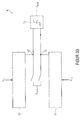
- FIG. 3 An exemplary solution of the equation system will be referred to Fig. 3 described using a concrete embodiment or an application example of the above-described digital-to-analog converter.
- Fig. 3a an analog-to-digital converter is shown, which includes a digital-to-analog converter, comparable to that described above, while Fig. 3b shows a modification of this analog-to-digital converter with two of the above digital-to-analog converters.
- Fig. 3a shows an analog-to-digital converter 40 having a digital-to-analog converter 10 'and a comparator 42 which is connected to a signal input to the summing junction 16 of the digital-to-analog converter 10'.
- the digital output D comp of the comparator 42 is connected via the calibration unit 12, which may be designed, for example, as an FPGA or generally comprise a CPU, which is designed to carry out the calibration algorithm described above.
- the calibration unit 12 is, as described above, with the elements for selective switching the capacitances (electrical components) 22a'-22c 'and 32a'-32c' of the digital-to-analog converter 10 'are coupled (see signal line 18).
- the digital-to-analogue converter 10 ' again a 6-bit digital-to-analogue converter, comprises the MSB field 20' and the LSB field 30 ', the electrical components 22a'-22c' and 32a'-32c 'are designed as capacities.
- the above design of the capacities depending on C 0 or depending on C UNIT is still valid.
- the dimensioning of C COUPLING or the coupling element 14 is analogous to that described above.
- An essential difference between the digital-to-analog converter 10 'and the digital-to-analog converter 10 is that the circuit of the electrical components 22a'-22c' or 32a'-32c 'by means of two different switching voltages, namely V REF + and V REF- done.
- These two switching signal sources or voltage sources are each arranged on a first side of the respective electrical switching element 22a'-22c 'or 32a'-32c' or linked to a switch with respect to a capacitor plate, so that with the two switching signals or voltages V REF + and V REF- the individual electrical switching elements 22a'-22c 'and 32a'-32c' are selectively activated or deactivated.
- the respective electrical components 22a'-22c 'or 32a'-32c' are activated via the switching elements (double switches) 24a'-24c 'or 34a'-34c' by means of the switching signal V REF + , while deactivation by means of the switching signal V REF- takes place.
- the switching signal V REF - switched to the respective electrical components 22a'-22c 'and 32a'-32c', while using a binary 1
- the regular switching signal V REF + are switched to the respective switching elements 22a'-22c 'and 32a'-32c', respectively.
- V REF - may, but does not necessarily have to, be the inverted switching signal to V REF + , but should at least be smaller in relation to the absolute value of V REF + .
- the measurement signal V IN to be quantified is applied to the first side of the electrical components 22a'-22c 'or 32a'-32c'.
- the application is effected by means of a switch (see Figures 25a-25c, 35a-35c), so that the signal or the charges which occur as a result of the application of the signal V IN can be stored.
- a switch see Figures 25a-25c, 35a-35c
- the second side of the electrical components 22a'-22c ' is coupled in the process of reading and storing the measurement signal V IN with a reference signal V CM for the MSB field 20' and V LSB for the LSB field 30 ', so that the measurement signal V in against these signals can be applied.
- the summation point 16 or the summation point 26 is connected in a switchable manner (switch 17) to a reference voltage source V CM
- the summing junction 36 is connected in a switchable manner (switch 37) to a reference voltage source V LSB .
- V LSB may be equal to V CM , but need not.
- the reference signal V C is typically applied to the second comparator input of the comparator 42.
- the implementation in the analog-to-digital conversion is typically as follows.
- the capacitors 22a'-22c 'and 32a'-32c' are connected via the switches 25a-25c, 35a-35c to the measuring signal V IN , so that the capacitances 22a'-22c 'and 32a'-32c' are connected through the Voltage difference between V in and the respective reference signal V LSB or V CM , if these are coupled to the respective summation points (LSB sum point 36 or MSB summation point 32) (compare switches 17 and 37) can be loaded.
- the switches 25a-25c, 35a-35c, 17, 37 are opened for V IN , V LSB and V CM , leaving the charge on the capacitance assembly 20 'plus 30' to be measured in a next step can be.
- the measuring signal is measured with the aid of the comparator 42, which, for example, compares the electrical voltage at the summing junction 16 with V CM and thus determines whether the electrical signal at 16 'is greater or smaller than the applied value V CM .
- the post-processing device can be based, for example, on the mathematical operators sum and / or addition, so as to correct the result of the AD conversion bit by bit, taking into account the correction values determined for the DA converter. It should be noted that the correction values are typically independent of the offset of the comparator 42 but dependent on C COUPLE , the influence of C COUPLE disappearing as it is the same in all correction values.
- the first calibration method basically corresponds to the method described above and may be referred to as foreground calibration.
- a predetermined code eg code 1
- the binary value of the MSB field 20 ' is changed by one step. It depends on the given code (code 1) whether the value of the MSB field 20 'is increased or decreased.
- the LSB codes (first and second LSB code or codes 2 and 3) are determined using the normal algorithm.
- the difference between the two binary LSB codes is stored as correction values.
- the predetermined code (code 1) is converted with the SAR algorithm, while the first LSB code thus determined (code 2) is used for the difference formation with the second LSB code (code 3).
- code 1 the predetermined code
- code 2 the first LSB code thus determined
- code 3 the difference formation with the second LSB code
- This calibration variant is referred to as background calibration and is preferably used when it is to be expected that the input signals V IN have a sufficiently large variance.
- the analog-to-digital converter 40 is operated to convert the input signal V IN .
- the algorithm for quantification is changed so that a second conversion of the same signal is possible.
- This algorithm can be accelerated according to additional embodiments by limiting the set of possible solutions for the second MSB combination.
- the search algorithm during calibration is designed to take into account the limitation of the second MSB combination.
- the starting of the individual MSB combinations depends on the measurement signal V IN . Due to this, it may happen that a tolerance value of the same electric component or the same electric component group is obtained several times.
- the old value can be replaced by the new one or, according to a second variant, the second values can be offset against each other (eg averaging, weighted averaging). In this way, fluctuations in the calibration values can be compensated for over time.
- both the foreground and background calibrations provide correction values for switching C 0 , switching C 0 + C 1, and switching C 0 + C 1 + C 2 .
- These values D0, D01, and D012 are now applied in normal operation to correct the output bitstream of the ADC.
- the determination of the correction values D0, D01 and D012 will now be described with reference to a mathematical example.
- A0, A1 and A2 are the MSB bits of the MSB combination which can take the values 0 and 1.
- D0, D1 and D2 are also the values of the MSB combination, whereby here the value range comprises -1 or 1.
- ALSB1 are the LSB bits of the LSB combination at the start of the calibration, while ALSB2 are the LSB bits after the conversion.
- n_ : Total ⁇ Table ⁇ 0 - Vin ⁇ 2 ⁇ ⁇ i Cu ⁇ 1 + subscript e i . i . 0 . n - 1 + 0 - 0 CCU
- ChargeLSBconv n_ : Total ⁇ Table ⁇ V LSB - subscript a . LSB ⁇ 2 * V REF ⁇ 2 ⁇ ⁇ i Cu . i . 0 .
- n_ : Total ⁇ Table ⁇ 0 - subscript a . LSB ⁇ 1 * V REF ⁇ 2 ⁇ ⁇ i Cu . i . 0 . n - 1 + 0 - 0 CCU
- A_LSB1 is the LSB binary code during sampling
- A_LSB2 is the LSB binary code still to be converted.
- A_LSB1 is the LSB binary code during sampling
- A_LSB2 is the LSB binary code still to be converted.
- d12 is the difference of A_LSB1-A_LSB2 when switching the MSB field from 1 to 2
- Fig. 3a shown analog-to-digital converter, which is designed to process a single-ended signal, can also be configured to process differential signals, as in Fig. 3b is shown.
- Fig. 3b 1 shows an analog-to-digital converter 40 'with the comparator 42 and two digital-to-analog converters 10' and 10 ' x .
- the first of the two digital-to-analog converters 10' is above the summing junction 16 with a first input of the comparator 42 coupled to the same, while the digital-to-analog converter 10 ' x is coupled to the second comparator input via the summing junction 16 x .
- a reference voltage source (see V CM ) can be provided, which can be connected in a switchable manner to the summing points 16 and 16 x .
- the first measurement signal part V IN1 is applied to the first digital-to-analog converter 10 ', while the second measurement signal part V IN2 is applied via the second digital-to-analog converter 10' x .
- the two digital-to-analog converters 10 'and 10' x are basically operated analogously to the above embodiment, but in each case the inverted switching signals V REF + and V REF- abut in the implementation.
- the MSB / LSB fields comprise at least three switchable electrical components
- the number per field may also vary, so that at least two electrical components, but preferably a plurality of electrical components Components are provided per MSB or LSB field. That is, for example, a C2C architecture for realizing the digital-to-analog converter would be possible, to which also the above-described method for calibration is applicable.
- the number of component fields used is not limited to the two (MSB and LSB device array).
- a further or more further LSB component fields can be provided which can be used for the calibration of the MSB field or else for the calibration of higher order LSB fields.
- resistors for the electrical components in the MSB, the LSB field and the electrical component for coupling the two fields.
- the resistance value R then corresponds to the conductance x. It is also pointed to the so-called R2R architecture, which also allows a realization of a digital-to-analog converter and can be calibrated according to the method described above.
- the electrical components may also be arranged according to another mathematical sequence. It is thus possible, for example, for the individual value ranges to overlap, which has an influence on the calibration insofar as the number of redundant values increases here. In the case of a mathematical sequence that is not completely occupied, the reverse effect occurs, so that not every value can be represented redundantly or not every value can be represented. In such varied weights of the dimensions of the electrical components of the digital-to-analog converter, the principle described above is equally applicable.
- a further switch can be provided, which connects the respective component 22a-22c , thereby a further switching voltage.
- the measurement signal V IN does not necessarily have to be applied via the digital-to-analog converter, but that it is also possible to apply the measurement signal, for example via the reference signal input of the comparator 42, ie via the second comparator input.
- a sample-hold circuit could be provided at the comparator input.
- the electrical components (22a-22c, 32a-32c, 22a'-22c ', 32a'-32c') and the coupling element (14, 14 ') each comprise at least one capacitor.
- the first and second electrical signal is a voltage signal.
- the number of electrical components of the MSB field (20, 20 ') which can be switched on the basis of the MSB combination equals the number of electrical components (32a-32c, 32a').
- the conductance values x n of the electrical components (22a-22c, 22a'-22c ') of the MSB field (20, 20') are similar in their tolerances to conductivities x n of the electrical components (32a-32c , 32a'-32c ') of the LSB field (30, 30').
- the MSB array (20, 20 ') and the LSB array (30, 30') each comprise at least three electrical components based on the MSB combination and / or based on the LSB combination are switchable.
- the digital-analog converter (10, 10 ') comprises a further LSB field (30, 30') with a third plurality of the electrical components (22a-22c, 32a-32c , 22a'-22c ', 32a'-32c'), which via a further coupling element (14, 14 ') with the LSB field (30, 30') and the MSB field (20, 20 ') to a parallel circuit is coupled.
- the calibration unit (12) is designed so that, when the first MSB combination (120) is varied, the first MSB combination is surrounded by a tolerance-afflicted least bit value for the MSB field (20, 20 '). ) to vary.
- the first tolerance value is assigned to the electrical component of the MSB field (20, 20 ') having the lowest bit significance.
- the further tolerance value is assigned to the group of electrical components (22a-22c, 22a'-22c ') of the MSB field (20, 20') which at least is assigned to the least significant bit value electrical component and the next higher Bitwertmaschine associated electrical component comprises.
- the calibration unit (12) is designed to be each electrical component of the MSB field (20, 20 ') to be calibrated and / or for each group of electrical components (22a-22c , 22a'-22c ') of the MSB field (20, 20') specify a first MSB combination.
- the calibration unit (12) is designed to vary the first LSB combination so as to determine the first electrical signal to be adjusted starting from the first MSB combination until the first MSB Combination together with the first LSB combination results in a first electrical signal at the summing junction (16); and / or the calibration unit (12) is designed to vary the second LSB combination for determining the resulting second electrical signal starting from the second MSB combination until the second MSB combination together with the second LSB combination to a second electrical signal at the summing junction (16).
- the calibration unit (12) is designed to use, as the first MSB combination and as the first LSB combination, a combination that is one of a combination is dependent on a measuring signal input of the digital-to-analog converter (10, 10 ') applied electrical measuring signal (V IN ).
- the calibration unit (12) comprises a buffer which, depending on the respective MSB combination, the first tolerance value and / or the further tolerance value for a plurality of electrical components (22a-22c, 22a'-22c ') of the MSB field (20, 20') stores, so that on the basis of the plurality of tolerance values for each electrical component of the MSB field (20, 20 '), a specific tolerance value can be calculated.
- the calibration unit (12) is designed to be specific to the electrical components (22a-22c, 22a'-22c ') on the basis of a system of equations which comprises at least as many equations as tolerance values. to calculate the tolerance values assigned to the MSB field (20, 20 ').
- the first tolerance value and the further tolerance value are a value dependent on a conductance for the coupling element (14, 14 ').
- the calibration unit (12) is designed to detect a multiplicity of determined and calculated, the individual electrical components (22a-22c, 22a'-22c ') of the MSB field (20, 20 '), to obtain an averaged selective tolerance value.
- the calibration unit (12) is designed to use the comparator (42) with the summation point (16) using a comparator (42) which comprises a measurement signal input determine first and second electrical signal.
- the electrical components (22a-22c, 32a-32c, 22a'-22c ', 32a'-32c') of the MSB field (20, 20 ') and the electrical components (32a) comprise 32c, 32a'-32c ') of the LSB field (30, 30') resistors, respectively.
- a twenty-fourth embodiment provides an analog-to-digital converter (40, 40 ') having the following features, a comparator (42); and a digital-to-analog converter (10, 10 ') according to one of the first to twenty-third embodiments, wherein the digital-to-analog converter (10, 10') is connected to a measuring signal input of the comparator (42) to the summing junction (16) is, so that a successive approximation analog-to-digital converter (40, 40 ') is formed.
- the calibration unit (12) is connected to the digital output of the comparator (42), depending on the output digital signal during calibration, the electrical components (32a-32c, 32a'-32c ') of LSB field (30, 30 ') selectively activate and / or deactivate.
- the measurement signal input of the analog-to-digital converter (40, 40 ') is formed by the digital-to-analog converter (10, 10'), and the electrical components (22a-22c, 32a -32c, 22a'-22c ', 32a'-32c') of the MSB field (20, 20 ') and the LSB field (30, 30') are connected in a switchable manner on a first side of the electrical components (22a-22c). 22c, 32a-32c, 22a'-22c ', 32a'-32c') can be acted upon by means of the electrical measuring signal (V IN ) to be determined.
- V IN electrical measuring signal
- the electrical components (22a-22c, 32a-32c, 22a'-22c ', 32a'-32c') of the MSB array (20, 20 ') and the LSB array (30th) comprise , 30 ') capacities, so a sample-and-hold circuit functionality is realized by the digital-to-analog converter (10, 10 ').
- the analog-to-digital converter (40, 40 ') is designed to use one of the MSB combination and / or the LSB as the digitized value of the electrical measurement signal to be determined (V IN ). Output combination dependent combination.
- the analog-to-digital converter (40, 40 ') comprises a post-processing unit which is designed to combine based on the first tolerance value and / or on the basis of the further tolerance value and / or on the basis of selective to rework the tolerance values assigned to the respective electrical components (22a-22c, 22a'-22c ') of the MSB field (20, 20').
- the MSB field (20, 20 ') comprises a reference voltage input, via which the electrical components (22a-22c, 22a'-22c') of the MSB field (20, 20 ') ) can be acted upon in a switchable manner with a reference voltage (V CM ), wherein the reference voltage input (V CM ) on a second, the first side opposite side of the electrical components (22a-22c, 22a'-22c ') of the MSB field (20 , 20 ') is arranged.
- V CM reference voltage input
- the reference voltage (V CM ) is provided by a voltage source which also forms the reference voltage (V CM ) for the comparator (42).
- the LSB field (30, 30 ') comprises a further reference voltage input (V LSB ), via which the electrical components (32a-32c, 32a'-32c') of the LSB field (30, 30 ') in a switchable manner with a further reference voltage (V LSB ) can be acted upon, wherein the reference voltage input on a second, the first side opposite side of the electrical components (22a-22c, 32a-32c, 22a'-22c'32a'-32c') of the LSB field (30, 30') is arranged.
- V LSB further reference voltage input
- the calibration unit (12) is designed to perform the calibration on the basis of a multiplicity of different electrical measurement signals (V IN ) applied to the measurement signal input, each of which has a first combination of the first MSB combination and the first LSB combination, and a second combination of the second MSB combination and the second LSB combination.
- V IN electrical measurement signals
- the measurement signal input of the analog-to-digital converter (40, 40 ') is formed by a further measurement signal input of the comparator (42), via which the electrical measurement signal (V IN ) to be determined corresponds to the analog measurement signal.
- Digital converter can be fed.
- the measurement signal input of the analog-to-digital converter (40, 40 ') comprises a sample and hold circuit.
- the step of determining the first electrical signal comprises repeatedly varying the first LSB combination in response to the first MSB combination, wherein the first LSB combination is varied until the first MSB combination together with the first LSB combination results in a first electrical signal at the summing junction (16), and wherein the step of determining the second electrical signal comprises repeatedly varying the second LSB combination in response to the second MSB combination, the second LSB -Combination is varied until the second MSB combination together with the second LSB combination leads to a second electrical signal at the summing junction (16).
- the first tolerance value for the electrical component of the MSB field (20, 20 ') having the lowest bit weight is determined based on a difference between the first and second LSB combinations when that for calibration the electrical component of the MSB field (20, 20 ') with the lowest bit weight, first and second MSB combination is selected; and or the further tolerance value for the group of electrical components (22a-22c, 22a'-22c ') of the MSB field (20, 20') can be determined on the basis of a difference between the first and second LSB combination, if the calibration used for Group of electrical components (22a-22c, 22a'-22c ') of the MSB field (20, 20'), first and second MSB combination is selected.
- the method (100) is performed in parallel with the detection of a plurality of measurement signals (V IN ) to be detected.
- the method (100) comprises the step of solving a system of equations (140) comprising at least as many equations as tolerance values after the step of determining the respective tolerance values to be specific ones electrical components (22a-22c, 22a'-22c ') of the MSB field (20, 20') to calculate associated tolerance values.
- a forty-first embodiment provides a computer program having a program code for performing the method of any one of the thirty-sixth to fortieth embodiments when the program is run on a CPU.
- aspects have been described in the context of a device, it will be understood that these aspects also constitute a description of the corresponding method, so that a block or a component of a device is also to be understood as a corresponding method step or as a feature of a method step. Similarly, aspects described in connection with or as a method step also represent a description of a corresponding block or detail or feature of a corresponding device.
- Some or all of the method steps may be performed by a hardware device (or using a hardware device). Apparatus), such as a microprocessor, a programmable computer or an electronic circuit. In some embodiments, some or more of the most important method steps may be performed by such an apparatus.
- embodiments of the invention may be implemented in hardware or in software.
- the implementation may be performed using a digital storage medium, such as a floppy disk, a DVD, a Blu-ray Disc, a CD, a ROM, a PROM, an EPROM, an EEPROM or FLASH memory, a hard disk, or other magnetic disk or optical memory are stored on the electronically readable control signals that can cooperate with a programmable computer system or cooperate such that the respective method is performed. Therefore, the digital storage medium can be computer readable.
- some embodiments according to the invention include a data carrier having electronically readable control signals capable of interacting with a programmable computer system such that one of the methods described herein is performed.
- embodiments of the present invention may be implemented as a computer program product having a program code, wherein the program code is operable to perform one of the methods when the computer program product runs on a computer.
- the program code can also be stored, for example, on a machine-readable carrier.
- inventions include the computer program for performing any of the methods described herein, wherein the computer program is stored on a machine-readable medium.
- an embodiment of the method according to the invention is thus a computer program which has a program code for performing one of the methods described herein when the computer program runs on a computer.
- a further embodiment of the inventive method is thus a data carrier (or a digital storage medium or a computer-readable medium) on which the computer program is recorded for carrying out one of the methods described herein.
- a further embodiment of the method according to the invention is thus a data stream or a sequence of signals, which represent the computer program for performing one of the methods described herein.
- the data stream or the sequence of signals may be configured, for example, to be transferred via a data communication connection, for example via the Internet.
- Another embodiment includes a processing device, such as a computer or a programmable logic device, that is configured or adapted to perform one of the methods described herein.
- a processing device such as a computer or a programmable logic device, that is configured or adapted to perform one of the methods described herein.
- Another embodiment includes a computer on which the computer program is installed to perform one of the methods described herein.
- Another embodiment according to the invention comprises a device or system adapted to transmit a computer program for performing at least one of the methods described herein to a receiver.
- the transmission can be done for example electronically or optically.
- the receiver may be, for example, a computer, a mobile device, a storage device or a similar device.
- the device or system may include a file server for transmitting the computer program to the recipient.
- a programmable logic device eg, a field programmable gate array, an FPGA
- a field programmable gate array may cooperate with a microprocessor to perform one of the methods described herein.
- the methods are performed by any hardware device. This may be a universal hardware such as a computer processor (CPU) or hardware specific to the process, such as an ASIC.
Landscapes
- Physics & Mathematics (AREA)
- Nonlinear Science (AREA)
- Engineering & Computer Science (AREA)
- Theoretical Computer Science (AREA)
- Analogue/Digital Conversion (AREA)
Applications Claiming Priority (1)
| Application Number | Priority Date | Filing Date | Title |
|---|---|---|---|
| DE102014200624.4A DE102014200624B3 (de) | 2014-01-15 | 2014-01-15 | Digital-Analog-Wandler, Analog-Digital-Wandlern und Verfahren zur Kalibrierung eines Digital-Analog-Wandlers |
Publications (1)
| Publication Number | Publication Date |
|---|---|
| EP2897293A1 true EP2897293A1 (fr) | 2015-07-22 |
Family
ID=52302166
Family Applications (1)
| Application Number | Title | Priority Date | Filing Date |
|---|---|---|---|
| EP15151291.0A Withdrawn EP2897293A1 (fr) | 2014-01-15 | 2015-01-15 | Convertisseur numérique/analogique et procédé d'étalonnage d'un convertisseur numérique/analogique |
Country Status (2)
| Country | Link |
|---|---|
| EP (1) | EP2897293A1 (fr) |
| DE (1) | DE102014200624B3 (fr) |
Cited By (1)
| Publication number | Priority date | Publication date | Assignee | Title |
|---|---|---|---|---|
| CN109802674A (zh) * | 2017-11-17 | 2019-05-24 | 比亚迪股份有限公司 | 逐次逼近模数转换器及其数字校准方法和装置 |
Families Citing this family (1)
| Publication number | Priority date | Publication date | Assignee | Title |
|---|---|---|---|---|
| WO2017101998A1 (fr) * | 2015-12-16 | 2017-06-22 | Huawei Technologies Co., Ltd. | Convertisseur de données étalonnable |
Citations (3)
| Publication number | Priority date | Publication date | Assignee | Title |
|---|---|---|---|---|
| US4970514A (en) | 1987-12-14 | 1990-11-13 | Siemens Aktiengesellschaft | Calibration method for redundant A/D and D/A converters with a weighted network |
| US20070075884A1 (en) * | 2005-09-30 | 2007-04-05 | Melanson John L | Calibration of a redundant number system successive approximation analog-to-digital converter |
| WO2012123578A1 (fr) * | 2011-03-17 | 2012-09-20 | Anacatum Design Ab | Étalonnage d'un can |
Family Cites Families (1)
| Publication number | Priority date | Publication date | Assignee | Title |
|---|---|---|---|---|
| US7746262B2 (en) * | 2005-12-19 | 2010-06-29 | Silicon Laboratories Inc. | Coding method for digital to analog converter of a SAR analog to digital converter |
-
2014
- 2014-01-15 DE DE102014200624.4A patent/DE102014200624B3/de not_active Expired - Fee Related
-
2015
- 2015-01-15 EP EP15151291.0A patent/EP2897293A1/fr not_active Withdrawn
Patent Citations (3)
| Publication number | Priority date | Publication date | Assignee | Title |
|---|---|---|---|---|
| US4970514A (en) | 1987-12-14 | 1990-11-13 | Siemens Aktiengesellschaft | Calibration method for redundant A/D and D/A converters with a weighted network |
| US20070075884A1 (en) * | 2005-09-30 | 2007-04-05 | Melanson John L | Calibration of a redundant number system successive approximation analog-to-digital converter |
| WO2012123578A1 (fr) * | 2011-03-17 | 2012-09-20 | Anacatum Design Ab | Étalonnage d'un can |
Non-Patent Citations (2)
| Title |
|---|
| JUNKEI GOTOH ED - INSTITUTE OF ELECTRICAL AND ELECTRONICS ENGINEERS: "A SELF-CALIBRATING 16BIT 6US CMOS AUDIO ADC", PROCEEDINGS OF THE CUSTOM INTEGRATED CIRCUITS CONFERENCE. BOSTON, MAY 13 - 16, 1990; [PROCEEDINGS OF THE CUSTOM INTEGRATED CIRCUITS CONFERENCE], NEW YORK, IEEE, US, vol. CONF. 12, 13 May 1990 (1990-05-13), pages 621 - 624, XP000167808 * |
| MOTOHIRO NAKANO ET AL: "A CONTINUOUSLY CALIBRATING CHARGE REDISTRIBUTION A/D CONVERTER", ELECTRONICS & COMMUNICATIONS IN JAPAN, PART II - ELECTRONICS, WILEY, HOBOKEN, NJ, US, vol. 72, no. 12, December 1989 (1989-12-01), pages 96 - 104, XP000136858, ISSN: 8756-663X * |
Cited By (2)
| Publication number | Priority date | Publication date | Assignee | Title |
|---|---|---|---|---|
| CN109802674A (zh) * | 2017-11-17 | 2019-05-24 | 比亚迪股份有限公司 | 逐次逼近模数转换器及其数字校准方法和装置 |
| CN109802674B (zh) * | 2017-11-17 | 2021-07-16 | 比亚迪半导体股份有限公司 | 逐次逼近模数转换器及其数字校准方法和装置 |
Also Published As
| Publication number | Publication date |
|---|---|
| DE102014200624B3 (de) | 2015-03-12 |
Similar Documents
| Publication | Publication Date | Title |
|---|---|---|
| DE102004058749B4 (de) | Vorrichtung zur Erfassung einer A/D-Wandler-Abnormität | |
| DE102009005770B4 (de) | SAR-ADC und Verfahren mit INL-Kompensation | |
| DE112009002259B4 (de) | Einheitliche Architektur für einen Folding-Analog-Digital-Wandler | |
| DE112016003066B4 (de) | Eingebauter Selbsttest für einen ADC | |
| DE112016003065T5 (de) | Verstärkungskalibrierung für AD-Wandler mit externer Referenz | |
| DE102012019042B4 (de) | Analog-Digital-Wandler | |
| DE102020126629A1 (de) | Verfahren zum einbetten eines eld-dac in einem sar-quantisierer | |
| DE102015102050A1 (de) | Analog-digital-umwandlung | |
| EP0452609A1 (fr) | Convertisseur analogique-numérique intégré monolithique à haute résolution | |
| DE102019133402A1 (de) | Kalibrierung von verstärkung zwischen stufen bei einem doppelumsetzungs-analog-digital-wandler | |
| DE10314189B4 (de) | Verfahren und Vorrichtung zur Kalibrierung eines gewichteten Netzwerks | |
| DE19936327C2 (de) | Verfahren und Vorrichtung zur Durchführung von ratiometrischen Messungen unter Verwendung eines Analog/Digital- oder eines Digital/Analog-Umsetzers, Analog/Digital- oder Digital/Analog-Umsetzer, und Verfahren zum Betreiben eines Analog/Digital- oder Digital/Analog-Umsetzers | |
| DE102021213494A1 (de) | System und verfahren zum testen eines analog-digital-wandlers | |
| DE102018114091B4 (de) | Verfahren zur Datenwandlung, bei denen ein Zustand basierend auf zeitpunktzugehörigen Linearitätsparametern bestimmt wird, sowie Vorrichtungen und Systeme zur Datenwandlung, eingerichtet, einen Zustand basierend auf zeitpunktzugehörigen Linearitätsparametern zu bestimmen | |
| DE69924013T2 (de) | Kapazitiver paralleler analog-digitalwandler | |
| EP3141877A2 (fr) | Dispositif et procédé de fonctionnement de capteurs à infrarouge passif | |
| DE102014200624B3 (de) | Digital-Analog-Wandler, Analog-Digital-Wandlern und Verfahren zur Kalibrierung eines Digital-Analog-Wandlers | |
| EP1504531B1 (fr) | Convertisseur numerique-analogique comportant un circuit de test integre | |
| DE102021102512A1 (de) | Analog-Digital-Wandler mit geschaltetem Kondensator und Verfahren zum Betreiben | |
| DE102014117457A1 (de) | Stochastische codierung bei analog-digital-umsetzung | |
| DE102018126603A1 (de) | Rauschformungs-Analog/Digital-Umsetzer | |
| EP2190121A1 (fr) | Convertisseur analogique-numérique multicanal | |
| EP3981076A1 (fr) | Convertisseur analogique-numérique | |
| DE4125717C1 (en) | Correcting or calibrating characteristic curve of sequentially working A=D converter - addressing correction value stored in ROM for each digital internal state of converter | |
| EP1565991B1 (fr) | Convertisseur analogique-numerique |
Legal Events
| Date | Code | Title | Description |
|---|---|---|---|
| PUAI | Public reference made under article 153(3) epc to a published international application that has entered the european phase |
Free format text: ORIGINAL CODE: 0009012 |
|
| 17P | Request for examination filed |
Effective date: 20150115 |
|
| AK | Designated contracting states |
Kind code of ref document: A1 Designated state(s): AL AT BE BG CH CY CZ DE DK EE ES FI FR GB GR HR HU IE IS IT LI LT LU LV MC MK MT NL NO PL PT RO RS SE SI SK SM TR |
|
| AX | Request for extension of the european patent |
Extension state: BA ME |
|
| 17P | Request for examination filed |
Effective date: 20160122 |
|
| RBV | Designated contracting states (corrected) |
Designated state(s): AL AT BE BG CH CY CZ DE DK EE ES FI FR GB GR HR HU IE IS IT LI LT LU LV MC MK MT NL NO PL PT RO RS SE SI SK SM TR |
|
| STAA | Information on the status of an ep patent application or granted ep patent |
Free format text: STATUS: REQUEST FOR EXAMINATION WAS MADE |
|
| STAA | Information on the status of an ep patent application or granted ep patent |
Free format text: STATUS: THE APPLICATION IS DEEMED TO BE WITHDRAWN |
|
| 18D | Application deemed to be withdrawn |
Effective date: 20180801 |