EP2899802A1 - Kombiniertes Streifenleitungschaltungssystem mit Blitzschutz - Google Patents
Kombiniertes Streifenleitungschaltungssystem mit Blitzschutz Download PDFInfo
- Publication number
- EP2899802A1 EP2899802A1 EP15150480.0A EP15150480A EP2899802A1 EP 2899802 A1 EP2899802 A1 EP 2899802A1 EP 15150480 A EP15150480 A EP 15150480A EP 2899802 A1 EP2899802 A1 EP 2899802A1
- Authority
- EP
- European Patent Office
- Prior art keywords
- length
- substrate
- circuit
- stripline
- circuitry
- Prior art date
- Legal status (The legal status is an assumption and is not a legal conclusion. Google has not performed a legal analysis and makes no representation as to the accuracy of the status listed.)
- Granted
Links
Images





Classifications
-
- H—ELECTRICITY
- H01—ELECTRIC ELEMENTS
- H01P—WAVEGUIDES; RESONATORS, LINES, OR OTHER DEVICES OF THE WAVEGUIDE TYPE
- H01P5/00—Coupling devices of the waveguide type
- H01P5/02—Coupling devices of the waveguide type with invariable factor of coupling
- H01P5/022—Transitions between lines of the same kind and shape, but with different dimensions
- H01P5/028—Transitions between lines of the same kind and shape, but with different dimensions between strip lines
-
- H—ELECTRICITY
- H01—ELECTRIC ELEMENTS
- H01P—WAVEGUIDES; RESONATORS, LINES, OR OTHER DEVICES OF THE WAVEGUIDE TYPE
- H01P1/00—Auxiliary devices
- H01P1/04—Fixed joints
- H01P1/047—Strip line joints
-
- H—ELECTRICITY
- H01—ELECTRIC ELEMENTS
- H01P—WAVEGUIDES; RESONATORS, LINES, OR OTHER DEVICES OF THE WAVEGUIDE TYPE
- H01P3/00—Waveguides; Transmission lines of the waveguide type
- H01P3/02—Waveguides; Transmission lines of the waveguide type with two longitudinal conductors
- H01P3/08—Microstrips; Strip lines
-
- H—ELECTRICITY
- H01—ELECTRIC ELEMENTS
- H01P—WAVEGUIDES; RESONATORS, LINES, OR OTHER DEVICES OF THE WAVEGUIDE TYPE
- H01P3/00—Waveguides; Transmission lines of the waveguide type
- H01P3/02—Waveguides; Transmission lines of the waveguide type with two longitudinal conductors
- H01P3/08—Microstrips; Strip lines
- H01P3/085—Triplate lines
-
- H—ELECTRICITY
- H01—ELECTRIC ELEMENTS
- H01Q—ANTENNAS, i.e. RADIO AERIALS
- H01Q1/00—Details of, or arrangements associated with, antennas
- H01Q1/50—Structural association of antennas with earthing switches, lead-in devices or lightning protectors
-
- H—ELECTRICITY
- H01—ELECTRIC ELEMENTS
- H01Q—ANTENNAS, i.e. RADIO AERIALS
- H01Q21/00—Antenna arrays or systems
- H01Q21/0006—Particular feeding systems
- H01Q21/0075—Stripline fed arrays
-
- H—ELECTRICITY
- H01—ELECTRIC ELEMENTS
- H01Q—ANTENNAS, i.e. RADIO AERIALS
- H01Q23/00—Antennas with active circuits or circuit elements integrated within them or attached to them
-
- H—ELECTRICITY
- H02—GENERATION; CONVERSION OR DISTRIBUTION OF ELECTRIC POWER
- H02H—EMERGENCY PROTECTIVE CIRCUIT ARRANGEMENTS
- H02H1/00—Details of emergency protective circuit arrangements
- H02H1/04—Arrangements for preventing response to transient abnormal conditions, e.g. to lightning or to short duration over voltage or oscillations; Damping the influence of DC component by short circuits in AC networks
-
- H—ELECTRICITY
- H05—ELECTRIC TECHNIQUES NOT OTHERWISE PROVIDED FOR
- H05K—PRINTED CIRCUITS; CASINGS OR CONSTRUCTIONAL DETAILS OF ELECTRIC APPARATUS; MANUFACTURE OF ASSEMBLAGES OF ELECTRICAL COMPONENTS
- H05K1/00—Printed circuits
- H05K1/02—Details
- H05K1/14—Structural association of two or more printed circuits
- H05K1/142—Arrangements of planar printed circuit boards in the same plane, e.g. auxiliary printed circuit insert mounted in a main printed circuit
-
- H—ELECTRICITY
- H05—ELECTRIC TECHNIQUES NOT OTHERWISE PROVIDED FOR
- H05K—PRINTED CIRCUITS; CASINGS OR CONSTRUCTIONAL DETAILS OF ELECTRIC APPARATUS; MANUFACTURE OF ASSEMBLAGES OF ELECTRICAL COMPONENTS
- H05K3/00—Apparatus or processes for manufacturing printed circuits
- H05K3/36—Assembling printed circuits with other printed circuits
-
- H—ELECTRICITY
- H01—ELECTRIC ELEMENTS
- H01P—WAVEGUIDES; RESONATORS, LINES, OR OTHER DEVICES OF THE WAVEGUIDE TYPE
- H01P1/00—Auxiliary devices
- H01P1/30—Auxiliary devices for compensation of, or protection against, temperature or moisture effects ; for improving power handling capability
-
- H—ELECTRICITY
- H01—ELECTRIC ELEMENTS
- H01Q—ANTENNAS, i.e. RADIO AERIALS
- H01Q21/00—Antenna arrays or systems
- H01Q21/06—Arrays of individually energised antenna units similarly polarised and spaced apart
- H01Q21/08—Arrays of individually energised antenna units similarly polarised and spaced apart the units being spaced along or adjacent to a rectilinear path
-
- H—ELECTRICITY
- H05—ELECTRIC TECHNIQUES NOT OTHERWISE PROVIDED FOR
- H05K—PRINTED CIRCUITS; CASINGS OR CONSTRUCTIONAL DETAILS OF ELECTRIC APPARATUS; MANUFACTURE OF ASSEMBLAGES OF ELECTRICAL COMPONENTS
- H05K2201/00—Indexing scheme relating to printed circuits covered by H05K1/00
- H05K2201/09—Shape and layout
- H05K2201/09145—Edge details
- H05K2201/09181—Notches in edge pads
-
- H—ELECTRICITY
- H05—ELECTRIC TECHNIQUES NOT OTHERWISE PROVIDED FOR
- H05K—PRINTED CIRCUITS; CASINGS OR CONSTRUCTIONAL DETAILS OF ELECTRIC APPARATUS; MANUFACTURE OF ASSEMBLAGES OF ELECTRICAL COMPONENTS
- H05K2201/00—Indexing scheme relating to printed circuits covered by H05K1/00
- H05K2201/09—Shape and layout
- H05K2201/09818—Shape or layout details not covered by a single group of H05K2201/09009 - H05K2201/09809
- H05K2201/09845—Stepped hole, via, edge, bump or conductor
-
- Y—GENERAL TAGGING OF NEW TECHNOLOGICAL DEVELOPMENTS; GENERAL TAGGING OF CROSS-SECTIONAL TECHNOLOGIES SPANNING OVER SEVERAL SECTIONS OF THE IPC; TECHNICAL SUBJECTS COVERED BY FORMER USPC CROSS-REFERENCE ART COLLECTIONS [XRACs] AND DIGESTS
- Y10—TECHNICAL SUBJECTS COVERED BY FORMER USPC
- Y10T—TECHNICAL SUBJECTS COVERED BY FORMER US CLASSIFICATION
- Y10T29/00—Metal working
- Y10T29/49—Method of mechanical manufacture
- Y10T29/49002—Electrical device making
- Y10T29/49117—Conductor or circuit manufacturing
- Y10T29/49124—On flat or curved insulated base, e.g., printed circuit, etc.
- Y10T29/49126—Assembling bases
Definitions
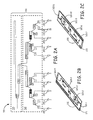
- Figure 2B is a diagram illustrating a first-portion 171 of the circuitry 110 of Figure 2A in and/or on a first printed circuit board (PCB) 210 according to one embodiment.
- the PCB 210 includes multiple layers.
- the first-portion 171 includes a first-driving-circuit portion of the driving circuit 150 of Figure 2A and a first-distribution-circuit portion of the power distribution circuit 160 of Figure 2A .
- the embodiments of the anti-lightning-combined-stripline-circuit systems described herein are based on the topology depicted in the '300 Application, however other the technology is application to a variety of other types of circuits.
- the technology described herein presents a design for the long length linear antenna array driven by a stripline with multiple layers.
- the circuitry 110 consists of two or more separate multilayer boards (e.g., first printed circuit board (PCB) 210 and second printed circuit board (PCB) 209) that are electrically connected to each other.
- the maximum length of the assembled board is able to reach up to twice the maximum size of the PCB material. For example, if the maximum size of PCB material is 48 inches, the driving length can be up to 96 inches.
- Figure 3 is a diagram illustrating four substrates 251-254 arranged with reference to each other prior to formation of a first-layered-stripline board 211 and a second-layered-stripline board 212 according to one embodiment.
- Figure 4 is a diagram illustrating a first-layered-stripline board 211 and a second-layered-stripline board 212 arranged with reference to each other prior to formation of a stripline board 115 for an anti-lightning-combined-stripline-circuit system 10 according to one embodiment.
- Figure 5 is a diagram illustrating a stripline board 115 for an anti-lightning-combined-stripline-circuit system 10 according to one embodiment.
- Figure 11 is an exemplary flow chart illustrating an exemplary method 1100 of forming a stripline board. The method 1100 is described with reference to Figures 2A-8B .
- Example 3 includes the anti-lightning-combined-stripline-circuit system of Example 2, further comprising: a first prepreg layer having a length equal to the second length, the first prepreg layer attaching the first substrate to the second substrate of the first-layered-stripline board; and a second prepreg layer having a length equal to the fourth length, the second prepreg layer attaching the third substrate to the fourth substrate of the second-layered-stripline board.
- Example 5 includes the anti-lightning-combined-stripline-circuit system of any of Examples 2-4, wherein the soldering region is a metal-coated U-shaped edge surface.
Landscapes
- Engineering & Computer Science (AREA)
- Microelectronics & Electronic Packaging (AREA)
- Manufacturing & Machinery (AREA)
- Power Engineering (AREA)
- Details Of Aerials (AREA)
- Emergency Protection Circuit Devices (AREA)
- Waveguides (AREA)
- Structure Of Printed Boards (AREA)
Applications Claiming Priority (1)
| Application Number | Priority Date | Filing Date | Title |
|---|---|---|---|
| US14/155,906 US9614268B2 (en) | 2014-01-15 | 2014-01-15 | Anti-lightning combined-stripline-circuit system |
Publications (2)
| Publication Number | Publication Date |
|---|---|
| EP2899802A1 true EP2899802A1 (de) | 2015-07-29 |
| EP2899802B1 EP2899802B1 (de) | 2017-11-01 |
Family
ID=52282644
Family Applications (1)
| Application Number | Title | Priority Date | Filing Date |
|---|---|---|---|
| EP15150480.0A Active EP2899802B1 (de) | 2014-01-15 | 2015-01-08 | Kombiniertes Streifenleitungschaltungssystem mit Blitzschutz |
Country Status (5)
| Country | Link |
|---|---|
| US (1) | US9614268B2 (de) |
| EP (1) | EP2899802B1 (de) |
| JP (1) | JP6608139B2 (de) |
| NO (1) | NO3051056T3 (de) |
| RU (1) | RU2681370C2 (de) |
Families Citing this family (2)
| Publication number | Priority date | Publication date | Assignee | Title |
|---|---|---|---|---|
| US11145977B2 (en) | 2019-06-14 | 2021-10-12 | Raytheon Company | Interlocking modular beamformer |
| US20210066830A1 (en) * | 2019-08-27 | 2021-03-04 | Raytheon Company | Stripline edge snap radio-frequency connection |
Citations (5)
| Publication number | Priority date | Publication date | Assignee | Title |
|---|---|---|---|---|
| GB2171257A (en) * | 1984-12-20 | 1986-08-20 | Marconi Co Ltd | A dipole array |
| WO1995023441A1 (en) * | 1994-02-28 | 1995-08-31 | Hazeltine Corporation | Slot array antennas |
| US5808529A (en) * | 1996-07-12 | 1998-09-15 | Storage Technology Corporation | Printed circuit board layering configuration for very high bandwidth interconnect |
| US5929822A (en) * | 1995-08-22 | 1999-07-27 | Marconi Aerospace Systems Inc. | Low intermodulation electromagnetic feed cellular antennas |
| US20080110020A1 (en) * | 2006-11-10 | 2008-05-15 | Heisen Peter T | Stripline flex circuit |
Family Cites Families (10)
| Publication number | Priority date | Publication date | Assignee | Title |
|---|---|---|---|---|
| US5471181A (en) | 1994-03-08 | 1995-11-28 | Hughes Missile Systems Company | Interconnection between layers of striplines or microstrip through cavity backed slot |
| JPH08340211A (ja) * | 1995-06-12 | 1996-12-24 | Sumitomo Electric Ind Ltd | アレイアンテナ |
| JP3314676B2 (ja) * | 1997-08-06 | 2002-08-12 | 日立電線株式会社 | ダイバーシチアンテナ |
| US6362787B1 (en) * | 1999-04-26 | 2002-03-26 | Andrew Corporation | Lightning protection for an active antenna using patch/microstrip elements |
| RU2210845C1 (ru) * | 2002-01-23 | 2003-08-20 | Федеральное государственное унитарное предприятие "Российский институт радионавигации и времени" | Антенный модуль для приема сигналов спутниковых систем и его усилительный блок |
| US6753814B2 (en) * | 2002-06-27 | 2004-06-22 | Harris Corporation | Dipole arrangements using dielectric substrates of meta-materials |
| US6965279B2 (en) | 2003-07-18 | 2005-11-15 | Ems Technologies, Inc. | Double-sided, edge-mounted stripline signal processing modules and modular network |
| GB0724684D0 (en) | 2007-12-18 | 2009-01-07 | Bae Systems Plc | Anntenna Feed Module |
| US8692728B2 (en) | 2012-01-01 | 2014-04-08 | Qualcomm Incorporated | Method for an antenna ground plane extension |
| US8912634B2 (en) | 2012-03-29 | 2014-12-16 | International Business Machines Corporation | High frequency transition matching in an electronic package for millimeter wave semiconductor dies |
-
2010
- 2010-01-22 NO NO16154337A patent/NO3051056T3/no unknown
-
2014
- 2014-01-15 US US14/155,906 patent/US9614268B2/en active Active
-
2015
- 2015-01-08 EP EP15150480.0A patent/EP2899802B1/de active Active
- 2015-01-13 RU RU2015100201A patent/RU2681370C2/ru not_active IP Right Cessation
- 2015-01-14 JP JP2015004855A patent/JP6608139B2/ja active Active
Patent Citations (5)
| Publication number | Priority date | Publication date | Assignee | Title |
|---|---|---|---|---|
| GB2171257A (en) * | 1984-12-20 | 1986-08-20 | Marconi Co Ltd | A dipole array |
| WO1995023441A1 (en) * | 1994-02-28 | 1995-08-31 | Hazeltine Corporation | Slot array antennas |
| US5929822A (en) * | 1995-08-22 | 1999-07-27 | Marconi Aerospace Systems Inc. | Low intermodulation electromagnetic feed cellular antennas |
| US5808529A (en) * | 1996-07-12 | 1998-09-15 | Storage Technology Corporation | Printed circuit board layering configuration for very high bandwidth interconnect |
| US20080110020A1 (en) * | 2006-11-10 | 2008-05-15 | Heisen Peter T | Stripline flex circuit |
Also Published As
| Publication number | Publication date |
|---|---|
| RU2681370C2 (ru) | 2019-03-06 |
| JP6608139B2 (ja) | 2019-11-20 |
| NO3051056T3 (de) | 2018-08-18 |
| US20150200434A1 (en) | 2015-07-16 |
| US9614268B2 (en) | 2017-04-04 |
| RU2015100201A (ru) | 2016-08-10 |
| EP2899802B1 (de) | 2017-11-01 |
| RU2015100201A3 (de) | 2018-08-30 |
| JP2015136109A (ja) | 2015-07-27 |
Similar Documents
| Publication | Publication Date | Title |
|---|---|---|
| CN106575808B (zh) | 传输线路及电子设备 | |
| US20150311591A1 (en) | Printed antenna having non-uniform layers | |
| US20190067805A1 (en) | Broadband conformal antenna | |
| EP2897216B1 (de) | Systeme und Verfahren für eine Antennenspeisung mit einer hängenden Streifenleitung | |
| US6133877A (en) | Microstrip distribution network device for antennas | |
| CN109075440B (zh) | 柔性印刷电路板结构体及室内分隔壁 | |
| EP2899802A1 (de) | Kombiniertes Streifenleitungschaltungssystem mit Blitzschutz | |
| DE69600976T2 (de) | Integrierte Flachantenne mit Umwandlungsfunktion | |
| EP3080864B1 (de) | Anordnung umfassend ein koaxialskabel und einen steckverbinder zur verbindung des koaxialkabels mit einer streifenleitung | |
| US11621464B2 (en) | Waveguide assembly | |
| US8704102B2 (en) | Printed flexible multilayer twisted-pair shielded high speed data cable | |
| KR101758043B1 (ko) | 인쇄 회로 기판들을 결합하기 위한 시스템 | |
| US10193206B2 (en) | Method of manufacturing a signal transition component having a C-shaped conducting frame | |
| WO2014121515A1 (en) | Integrated stripline feed network for linear antenna array | |
| DE102016204022A1 (de) | Vorrichtung zum Senden und/oder Empfangen elektromagnetischer Strahlung | |
| WO2022084024A1 (de) | Radarsensor | |
| EP0763870B1 (de) | Gruppenantenne mit aktiven Sende-/Empfangsmodulen | |
| DE10204568A1 (de) | Radargerät | |
| DE60037532T2 (de) | Anordnung zum schutz einer antenne | |
| KR20150044404A (ko) | 우주용 안테나 시스템 | |
| WO2004036688A1 (de) | Dielektrische patch-antenne | |
| KR930017235A (ko) | 저손실, 광대역 스트립라인-마이크로스트립 트랜지션 |
Legal Events
| Date | Code | Title | Description |
|---|---|---|---|
| PUAI | Public reference made under article 153(3) epc to a published international application that has entered the european phase |
Free format text: ORIGINAL CODE: 0009012 |
|
| 17P | Request for examination filed |
Effective date: 20150108 |
|
| AK | Designated contracting states |
Kind code of ref document: A1 Designated state(s): AL AT BE BG CH CY CZ DE DK EE ES FI FR GB GR HR HU IE IS IT LI LT LU LV MC MK MT NL NO PL PT RO RS SE SI SK SM TR |
|
| AX | Request for extension of the european patent |
Extension state: BA ME |
|
| RAP1 | Party data changed (applicant data changed or rights of an application transferred) |
Owner name: HONEYWELL INTERNATIONAL INC. |
|
| 17Q | First examination report despatched |
Effective date: 20160314 |
|
| GRAP | Despatch of communication of intention to grant a patent |
Free format text: ORIGINAL CODE: EPIDOSNIGR1 |
|
| RIC1 | Information provided on ipc code assigned before grant |
Ipc: H01P 3/08 20060101AFI20170530BHEP Ipc: H01Q 21/00 20060101ALI20170530BHEP Ipc: H01P 11/00 20060101ALI20170530BHEP Ipc: H01Q 21/08 20060101ALN20170530BHEP Ipc: H01P 1/04 20060101ALI20170530BHEP Ipc: H02H 1/04 20060101ALI20170530BHEP Ipc: H01P 1/30 20060101ALI20170530BHEP Ipc: H01P 5/02 20060101ALI20170530BHEP Ipc: H05K 1/14 20060101ALN20170530BHEP Ipc: H05K 3/36 20060101ALN20170530BHEP Ipc: H01Q 1/50 20060101ALI20170530BHEP |
|
| RIC1 | Information provided on ipc code assigned before grant |
Ipc: H01P 1/04 20060101ALI20170602BHEP Ipc: H05K 3/36 20060101ALN20170602BHEP Ipc: H01P 11/00 20060101ALI20170602BHEP Ipc: H05K 1/14 20060101ALN20170602BHEP Ipc: H01Q 1/50 20060101ALI20170602BHEP Ipc: H01Q 21/08 20060101ALN20170602BHEP Ipc: H01Q 21/00 20060101ALI20170602BHEP Ipc: H01P 3/08 20060101AFI20170602BHEP Ipc: H01P 5/02 20060101ALI20170602BHEP Ipc: H01P 1/30 20060101ALI20170602BHEP Ipc: H02H 1/04 20060101ALI20170602BHEP |
|
| INTG | Intention to grant announced |
Effective date: 20170620 |
|
| GRAS | Grant fee paid |
Free format text: ORIGINAL CODE: EPIDOSNIGR3 |
|
| GRAA | (expected) grant |
Free format text: ORIGINAL CODE: 0009210 |
|
| AK | Designated contracting states |
Kind code of ref document: B1 Designated state(s): AL AT BE BG CH CY CZ DE DK EE ES FI FR GB GR HR HU IE IS IT LI LT LU LV MC MK MT NL NO PL PT RO RS SE SI SK SM TR |
|
| REG | Reference to a national code |
Ref country code: GB Ref legal event code: FG4D |
|
| REG | Reference to a national code |
Ref country code: CH Ref legal event code: EP Ref country code: AT Ref legal event code: REF Ref document number: 942896 Country of ref document: AT Kind code of ref document: T Effective date: 20171115 |
|
| REG | Reference to a national code |
Ref country code: IE Ref legal event code: FG4D |
|
| REG | Reference to a national code |
Ref country code: DE Ref legal event code: R096 Ref document number: 602015005635 Country of ref document: DE |
|
| REG | Reference to a national code |
Ref country code: NO Ref legal event code: T2 Effective date: 20171101 |
|
| REG | Reference to a national code |
Ref country code: NL Ref legal event code: MP Effective date: 20171101 |
|
| REG | Reference to a national code |
Ref country code: LT Ref legal event code: MG4D |
|
| REG | Reference to a national code |
Ref country code: AT Ref legal event code: MK05 Ref document number: 942896 Country of ref document: AT Kind code of ref document: T Effective date: 20171101 |
|
| PG25 | Lapsed in a contracting state [announced via postgrant information from national office to epo] |
Ref country code: SE Free format text: LAPSE BECAUSE OF FAILURE TO SUBMIT A TRANSLATION OF THE DESCRIPTION OR TO PAY THE FEE WITHIN THE PRESCRIBED TIME-LIMIT Effective date: 20171101 Ref country code: ES Free format text: LAPSE BECAUSE OF FAILURE TO SUBMIT A TRANSLATION OF THE DESCRIPTION OR TO PAY THE FEE WITHIN THE PRESCRIBED TIME-LIMIT Effective date: 20171101 Ref country code: NL Free format text: LAPSE BECAUSE OF FAILURE TO SUBMIT A TRANSLATION OF THE DESCRIPTION OR TO PAY THE FEE WITHIN THE PRESCRIBED TIME-LIMIT Effective date: 20171101 Ref country code: LT Free format text: LAPSE BECAUSE OF FAILURE TO SUBMIT A TRANSLATION OF THE DESCRIPTION OR TO PAY THE FEE WITHIN THE PRESCRIBED TIME-LIMIT Effective date: 20171101 Ref country code: FI Free format text: LAPSE BECAUSE OF FAILURE TO SUBMIT A TRANSLATION OF THE DESCRIPTION OR TO PAY THE FEE WITHIN THE PRESCRIBED TIME-LIMIT Effective date: 20171101 |
|
| PG25 | Lapsed in a contracting state [announced via postgrant information from national office to epo] |
Ref country code: RS Free format text: LAPSE BECAUSE OF FAILURE TO SUBMIT A TRANSLATION OF THE DESCRIPTION OR TO PAY THE FEE WITHIN THE PRESCRIBED TIME-LIMIT Effective date: 20171101 Ref country code: IS Free format text: LAPSE BECAUSE OF FAILURE TO SUBMIT A TRANSLATION OF THE DESCRIPTION OR TO PAY THE FEE WITHIN THE PRESCRIBED TIME-LIMIT Effective date: 20180301 Ref country code: LV Free format text: LAPSE BECAUSE OF FAILURE TO SUBMIT A TRANSLATION OF THE DESCRIPTION OR TO PAY THE FEE WITHIN THE PRESCRIBED TIME-LIMIT Effective date: 20171101 Ref country code: AT Free format text: LAPSE BECAUSE OF FAILURE TO SUBMIT A TRANSLATION OF THE DESCRIPTION OR TO PAY THE FEE WITHIN THE PRESCRIBED TIME-LIMIT Effective date: 20171101 Ref country code: GR Free format text: LAPSE BECAUSE OF FAILURE TO SUBMIT A TRANSLATION OF THE DESCRIPTION OR TO PAY THE FEE WITHIN THE PRESCRIBED TIME-LIMIT Effective date: 20180202 Ref country code: BG Free format text: LAPSE BECAUSE OF FAILURE TO SUBMIT A TRANSLATION OF THE DESCRIPTION OR TO PAY THE FEE WITHIN THE PRESCRIBED TIME-LIMIT Effective date: 20180201 Ref country code: HR Free format text: LAPSE BECAUSE OF FAILURE TO SUBMIT A TRANSLATION OF THE DESCRIPTION OR TO PAY THE FEE WITHIN THE PRESCRIBED TIME-LIMIT Effective date: 20171101 |
|
| PG25 | Lapsed in a contracting state [announced via postgrant information from national office to epo] |
Ref country code: DK Free format text: LAPSE BECAUSE OF FAILURE TO SUBMIT A TRANSLATION OF THE DESCRIPTION OR TO PAY THE FEE WITHIN THE PRESCRIBED TIME-LIMIT Effective date: 20171101 Ref country code: CZ Free format text: LAPSE BECAUSE OF FAILURE TO SUBMIT A TRANSLATION OF THE DESCRIPTION OR TO PAY THE FEE WITHIN THE PRESCRIBED TIME-LIMIT Effective date: 20171101 Ref country code: CY Free format text: LAPSE BECAUSE OF FAILURE TO SUBMIT A TRANSLATION OF THE DESCRIPTION OR TO PAY THE FEE WITHIN THE PRESCRIBED TIME-LIMIT Effective date: 20171101 Ref country code: EE Free format text: LAPSE BECAUSE OF FAILURE TO SUBMIT A TRANSLATION OF THE DESCRIPTION OR TO PAY THE FEE WITHIN THE PRESCRIBED TIME-LIMIT Effective date: 20171101 Ref country code: SK Free format text: LAPSE BECAUSE OF FAILURE TO SUBMIT A TRANSLATION OF THE DESCRIPTION OR TO PAY THE FEE WITHIN THE PRESCRIBED TIME-LIMIT Effective date: 20171101 |
|
| REG | Reference to a national code |
Ref country code: DE Ref legal event code: R119 Ref document number: 602015005635 Country of ref document: DE |
|
| PG25 | Lapsed in a contracting state [announced via postgrant information from national office to epo] |
Ref country code: IT Free format text: LAPSE BECAUSE OF FAILURE TO SUBMIT A TRANSLATION OF THE DESCRIPTION OR TO PAY THE FEE WITHIN THE PRESCRIBED TIME-LIMIT Effective date: 20171101 Ref country code: RO Free format text: LAPSE BECAUSE OF FAILURE TO SUBMIT A TRANSLATION OF THE DESCRIPTION OR TO PAY THE FEE WITHIN THE PRESCRIBED TIME-LIMIT Effective date: 20171101 Ref country code: PL Free format text: LAPSE BECAUSE OF FAILURE TO SUBMIT A TRANSLATION OF THE DESCRIPTION OR TO PAY THE FEE WITHIN THE PRESCRIBED TIME-LIMIT Effective date: 20171101 Ref country code: SM Free format text: LAPSE BECAUSE OF FAILURE TO SUBMIT A TRANSLATION OF THE DESCRIPTION OR TO PAY THE FEE WITHIN THE PRESCRIBED TIME-LIMIT Effective date: 20171101 |
|
| REG | Reference to a national code |
Ref country code: CH Ref legal event code: PL |
|
| PLBE | No opposition filed within time limit |
Free format text: ORIGINAL CODE: 0009261 |
|
| STAA | Information on the status of an ep patent application or granted ep patent |
Free format text: STATUS: NO OPPOSITION FILED WITHIN TIME LIMIT |
|
| 26N | No opposition filed |
Effective date: 20180802 |
|
| PG25 | Lapsed in a contracting state [announced via postgrant information from national office to epo] |
Ref country code: LU Free format text: LAPSE BECAUSE OF NON-PAYMENT OF DUE FEES Effective date: 20180108 Ref country code: FR Free format text: LAPSE BECAUSE OF NON-PAYMENT OF DUE FEES Effective date: 20180131 Ref country code: DE Free format text: LAPSE BECAUSE OF NON-PAYMENT OF DUE FEES Effective date: 20180801 |
|
| REG | Reference to a national code |
Ref country code: IE Ref legal event code: MM4A |
|
| REG | Reference to a national code |
Ref country code: FR Ref legal event code: ST Effective date: 20180928 |
|
| REG | Reference to a national code |
Ref country code: BE Ref legal event code: MM Effective date: 20180131 |
|
| PG25 | Lapsed in a contracting state [announced via postgrant information from national office to epo] |
Ref country code: CH Free format text: LAPSE BECAUSE OF NON-PAYMENT OF DUE FEES Effective date: 20180131 Ref country code: BE Free format text: LAPSE BECAUSE OF NON-PAYMENT OF DUE FEES Effective date: 20180131 Ref country code: LI Free format text: LAPSE BECAUSE OF NON-PAYMENT OF DUE FEES Effective date: 20180131 Ref country code: SI Free format text: LAPSE BECAUSE OF FAILURE TO SUBMIT A TRANSLATION OF THE DESCRIPTION OR TO PAY THE FEE WITHIN THE PRESCRIBED TIME-LIMIT Effective date: 20171101 |
|
| PG25 | Lapsed in a contracting state [announced via postgrant information from national office to epo] |
Ref country code: IE Free format text: LAPSE BECAUSE OF NON-PAYMENT OF DUE FEES Effective date: 20180108 |
|
| PG25 | Lapsed in a contracting state [announced via postgrant information from national office to epo] |
Ref country code: MC Free format text: LAPSE BECAUSE OF FAILURE TO SUBMIT A TRANSLATION OF THE DESCRIPTION OR TO PAY THE FEE WITHIN THE PRESCRIBED TIME-LIMIT Effective date: 20171101 |
|
| GBPC | Gb: european patent ceased through non-payment of renewal fee |
Effective date: 20190108 |
|
| PG25 | Lapsed in a contracting state [announced via postgrant information from national office to epo] |
Ref country code: GB Free format text: LAPSE BECAUSE OF NON-PAYMENT OF DUE FEES Effective date: 20190108 |
|
| PG25 | Lapsed in a contracting state [announced via postgrant information from national office to epo] |
Ref country code: MT Free format text: LAPSE BECAUSE OF NON-PAYMENT OF DUE FEES Effective date: 20180108 |
|
| PG25 | Lapsed in a contracting state [announced via postgrant information from national office to epo] |
Ref country code: TR Free format text: LAPSE BECAUSE OF FAILURE TO SUBMIT A TRANSLATION OF THE DESCRIPTION OR TO PAY THE FEE WITHIN THE PRESCRIBED TIME-LIMIT Effective date: 20171101 |
|
| PG25 | Lapsed in a contracting state [announced via postgrant information from national office to epo] |
Ref country code: PT Free format text: LAPSE BECAUSE OF FAILURE TO SUBMIT A TRANSLATION OF THE DESCRIPTION OR TO PAY THE FEE WITHIN THE PRESCRIBED TIME-LIMIT Effective date: 20171101 |
|
| PG25 | Lapsed in a contracting state [announced via postgrant information from national office to epo] |
Ref country code: MK Free format text: LAPSE BECAUSE OF NON-PAYMENT OF DUE FEES Effective date: 20171101 Ref country code: HU Free format text: LAPSE BECAUSE OF FAILURE TO SUBMIT A TRANSLATION OF THE DESCRIPTION OR TO PAY THE FEE WITHIN THE PRESCRIBED TIME-LIMIT; INVALID AB INITIO Effective date: 20150108 |
|
| PG25 | Lapsed in a contracting state [announced via postgrant information from national office to epo] |
Ref country code: AL Free format text: LAPSE BECAUSE OF FAILURE TO SUBMIT A TRANSLATION OF THE DESCRIPTION OR TO PAY THE FEE WITHIN THE PRESCRIBED TIME-LIMIT Effective date: 20171101 |
|
| P01 | Opt-out of the competence of the unified patent court (upc) registered |
Effective date: 20230525 |
|
| PGFP | Annual fee paid to national office [announced via postgrant information from national office to epo] |
Ref country code: NO Payment date: 20260120 Year of fee payment: 12 |