EP2899838A1 - Circuit de commande de charge, appareil de charge, procédé de commande de charge et procédé de charge - Google Patents
Circuit de commande de charge, appareil de charge, procédé de commande de charge et procédé de charge Download PDFInfo
- Publication number
- EP2899838A1 EP2899838A1 EP13839677.5A EP13839677A EP2899838A1 EP 2899838 A1 EP2899838 A1 EP 2899838A1 EP 13839677 A EP13839677 A EP 13839677A EP 2899838 A1 EP2899838 A1 EP 2899838A1
- Authority
- EP
- European Patent Office
- Prior art keywords
- current
- voltage
- charging
- signal
- active
- Prior art date
- Legal status (The legal status is an assumption and is not a legal conclusion. Google has not performed a legal analysis and makes no representation as to the accuracy of the status listed.)
- Granted
Links
Images




Classifications
-
- H—ELECTRICITY
- H02—GENERATION; CONVERSION OR DISTRIBUTION OF ELECTRIC POWER
- H02J—ELECTRIC POWER NETWORKS; CIRCUIT ARRANGEMENTS OR SYSTEMS FOR SUPPLYING OR DISTRIBUTING ELECTRIC POWER; SYSTEMS FOR STORING ELECTRIC ENERGY
- H02J7/00—Circuit arrangements for charging or discharging batteries or for supplying loads from batteries
- H02J7/90—Regulation of charging or discharging current or voltage
- H02J7/96—Regulation of charging or discharging current or voltage in response to battery voltage
-
- H—ELECTRICITY
- H02—GENERATION; CONVERSION OR DISTRIBUTION OF ELECTRIC POWER
- H02J—ELECTRIC POWER NETWORKS; CIRCUIT ARRANGEMENTS OR SYSTEMS FOR SUPPLYING OR DISTRIBUTING ELECTRIC POWER; SYSTEMS FOR STORING ELECTRIC ENERGY
- H02J7/00—Circuit arrangements for charging or discharging batteries or for supplying loads from batteries
-
- H—ELECTRICITY
- H02—GENERATION; CONVERSION OR DISTRIBUTION OF ELECTRIC POWER
- H02J—ELECTRIC POWER NETWORKS; CIRCUIT ARRANGEMENTS OR SYSTEMS FOR SUPPLYING OR DISTRIBUTING ELECTRIC POWER; SYSTEMS FOR STORING ELECTRIC ENERGY
- H02J7/00—Circuit arrangements for charging or discharging batteries or for supplying loads from batteries
- H02J7/60—Circuit arrangements for charging or discharging batteries or for supplying loads from batteries including safety or protection arrangements
-
- H—ELECTRICITY
- H02—GENERATION; CONVERSION OR DISTRIBUTION OF ELECTRIC POWER
- H02J—ELECTRIC POWER NETWORKS; CIRCUIT ARRANGEMENTS OR SYSTEMS FOR SUPPLYING OR DISTRIBUTING ELECTRIC POWER; SYSTEMS FOR STORING ELECTRIC ENERGY
- H02J7/00—Circuit arrangements for charging or discharging batteries or for supplying loads from batteries
- H02J7/60—Circuit arrangements for charging or discharging batteries or for supplying loads from batteries including safety or protection arrangements
- H02J7/61—Circuit arrangements for charging or discharging batteries or for supplying loads from batteries including safety or protection arrangements against overcharge
Definitions
- the present invention relates to the field of charging and particularly to a charging control circuit and a charging apparatus, and a charging control method and a charging method, applicable to a charging scheme with adjustable output voltage and output current.
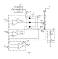
- Fig. 1 is a schematic structural diagram of an example of a charging apparatus in the prior art. As illustrated in Fig. 1 , the charging apparatus 1 configured to charge a battery 100 includes a charging execution circuit 11, a charging protection circuit 12 and a charging control circuit 13.
- the charging execution circuit 11 is configured to generate output voltage Vout and output current Iout at a charging output terminal thereof, and to adjust the generated output voltage Vout and output current Iout, in a period of charging.
- the charging execution circuit 11 includes differential amplifiers 111 and 112, a voltage selector 113 and an adjustable switch 114 (which is a PMOS in this context merely by way of an example); and the negative input terminal of the differential amplifier 111 is a current reference input terminal of the charging execution circuit 11, the negative input terminal of the differential amplifier 112 is a voltage reference input terminal of the charging execution circuit 11, and the drain D of the PMOS 114 is the charging output terminal of the charging execution circuit 11.
- the negative input terminal of the differential amplifier 111 receives an input nominal current reference Iref_s, the other positive input terminal of the differential amplifier 111 receives the output current Iout fed back at the charging output terminal of the differential amplifier 111, and the output terminal of the differential amplifier 111 outputs a control signal Ctrl_I at a positive voltage value, where the positive voltage value of the control signal Ctrl_I indicates a current difference of the output current Iout from the nominal current reference Iref_s;
- the negative input terminal of the differential amplifier 112 receives an input nominal voltage reference Vref_s
- the other positive input terminal of the differential amplifier 112 receives the output voltage Vout outputting by the charging output terminal of the differential amplifier 111
- the output terminal of the differential amplifier 112 outputs a control signal Ctrl_V at a positive voltage value, where the positive voltage value of the control signal Ctrl_V indicates a voltage difference of the output voltage Vout from the nominal voltage reference Vref_s;
- the voltage selector 113 receives the control signal Ctrl_I and the control signal Ctrl_V, and the voltage selector 113 further receives a control signal Ctrl_P output by the charging protection circuit 12 based on a charging status signal S (e.g., a signal indicating the status of a power source Vcc0, temperature inside the charging apparatus 1, temperature inside the battery 100, etc.); and, where a positive voltage value of the control signal Ctrl_P indcates abnormality or not, and typically the positive voltage value of the control signal Ctrl_P will become higher upon abnormality; and the voltage selector 113 selects the highest one of the positive voltage values of the control signal Ctrl_I, the control signal Ctrl_V and the control signal Ctrl_P (alternatively the lowest one can be selected in a practical application for a different characteristic of an element although the highest one is selected in this context by way of an example) and sets the gate G of the PMOS 114 at the selected highest positive
- the source S of the PMOS 114 is connected with the input power source Vcc0, and the drain D of the PMOS 114 is connected with the battery 100 and configured to generate the output current Iout and the output voltage Vout; and the conductivity between the source S and the drain D of the PMOS 114 can be adjusted with the varying positive voltage value of the gate G of the PMOS 114 to thereby adjust the output current Iout; and correspondingly since the output voltage Vout is equal to the sum of the kernel voltage V0 of the battery 100 and the voltage drop across the inner resistor R0 of the battery 100, and both the kernel voltage V0 and the voltage drop across the inner resistor R0 are dependent upon the output current Iout, so the output voltage Vout can be adjusted together with the adjustment of the output current Iout.
- the charging control circuit 13 is configured to control charging to be terminated based on whether the output current Iout is lower than a nominal current reference Iref_s'.
- the charging control circuit 13 includes a comparator 130.
- the negative input terminal of the comparator 130 receives the output current Iout fed back at the charging output terminal of the charging execution circuit 11, the other positive input terminal of the comparator 130 receives the nominal current reference Iref_s', and the output terminal of the comparator 130 generates a charging termination signal Fin_a; and when the output current Iout is lower than the nominal current reference Iref_s', the charging termination signal Fin_a is set at an active high level to trigger termination of charging by the charging execution circuit 11.
- the nominal current reference Iref_s is a well-known current reference for constant-current charging
- the nominal current reference Iref_s' is a well-known current reference for termination of charging
- the nominal current reference Iref_s is higher than the nominal current reference Iref_s'
- the nominal voltage reference Vref_s is a well-known voltage reference for termination of charging.
- the output current Iout is far lower than the nominal current reference Iref_s, and the output voltage Vout is far lower than the nominal voltage reference Vref_s, and at this time both the control signal Ctrl_I and the control signal Ctrl_V are at lower positive voltage values so that the voltage selector 112 will also set the gate G of the PMOS 114 at a lower positive voltage value; and then since the source S of the PMOS 114 is pulled high by the input power source Vcc0, the voltage difference VGS between the gate and the source of the PMOS 114 is at a negative value and lower than the cutoff voltage of the PMOS 114 so that the PMOS 114 becomes maximally conductive and the output current Iout becomes higher;
- the positive voltage value of the control signal Ctrl_I will be higher than that of the control signal Ctrl_V, and correspondingly the gate G of the PMOS 114 will be set by the voltage selector 112 at the positive voltage value of the control signal Ctrl_I, and the conductivity of the PMOS 114 will also be controlled by the positive voltage value of the Ctrl_I;
- the conductivity of the PMOS 114 controlled by the positive voltage value of the control signal Ctrl_I will have the output current Iout maintained at the nominal current reference Iref_s, and thereafter a constant-current charging phase will commence.
- the inner voltage V0 of the battery 100 will gradually become higher, and correspondingly the output voltage Vout will also gradually become higher from a lower voltage value far lower than the nominal voltage reference Vref_s; and since the positive voltage value of the control signal Ctrl_I will be maintained all the time at a positive voltage value indicating that the output current Iout reaches the nominal current reference Iref_s, the positive voltage value of the control signal Ctrl_V will be still lower than the positive voltage value of the control signal Ctrl_I as long as the output voltage Vout has not reached the nominal voltage reference Vref_s; and
- the positive voltage value of the control signal Ctrl_V will be higher than the positive voltage value of the control signal Ctrl_I, and then at this time the gate G of the PMOS 114 will be set by the voltage selector 112 at a higher positive voltage value of the control signal Ctrl_V so that the voltage difference VGS between the gate and the source of the PMOS 114 lower than the cutoff voltage will become higher and consequently the PMOS 114 will become less conductive and the output current Iout will become lower, and thereafter a constant-voltage charging phase will commence.
- the output voltage Vout will be equal to the nominal voltage reference Vref_s due to a negative feedback
- the charging termination signal Fin_a becomes an active high level to thereby trigger termination of charging (how to trigger termination of charging will be of no interest in this context, and those skilled in the art have appreciated a number of particular implementations thereof, so a repeated description thereof will be omitted here).
- the charging execution circuit 11 in the existing charging apparatus 1 can be used to implement a charging scheme in which the output voltage Vout and the output current Iout is adjustable, and the charging control circuit 13 thereof can be used to control charging to be terminated, but since the charging control circuit 13 in the existing charging apparatus 1 may unreasonably control charging to be terminated and the charging execution circuit 11 thereof can not be controlled to adjust the output voltage Vout and the output current Iout, the following drawbacks may arise:
- the invention provides a charging control circuit and a charging apparatus, and a charging control method and a charging method.
- a charging control circuit configured to control a charging execution circuit to adjust output voltage and output current generated at a charging output terminal thereof and to control charging by the charging execution circuit to be terminated, and the charging control circuit includes a current adjustment module and a detection control module, and wherein:
- the second current reference with the limitation removed is adjusted up by the current adjustment module; when the current difference higher than or equal to a preset second current threshold and lower than a preset third current threshold is detected in the period of charging, if the second current reference has not reached the lowest current value, then the second current reference with the limitation removed is adjusted down by the current adjustment module; and when the current difference higher than or equal to the third current threshold is detected in the period of charging, if the second current reference has not reached the lowest current value, then the second current reference with the limitation removed is reset to the lowest current value by the current adjustment module; and wherein the first current threshold is lower than the second current threshold, and the second current threshold is lower than the third current threshold; and/or
- the charging control circuit further includes a voltage adjustment module configured to adjust the first voltage reference and to output a second voltage reference as a result of adjustment to a voltage reference input terminal of the charging execution circuit to control the charging execution circuit to adjust the output voltage and the output current, and wherein the highest voltage value of the second voltage reference is higher than the first voltage reference, and the lowest voltage value thereof is equal to the first voltage reference; and the detection control circuit is further configured to control the voltage adjustment module so that: when the voltage difference higher than or equal to the first voltage threshold and lower than a second voltage threshold is detected at the end of the period of interruption, if the second voltage reference has not reached the lowest voltage value, then the second voltage reference is adjusted down by the voltage adjustment module; when the voltage difference higher than a third voltage threshold is detected at the end of the period of interruption, if the second voltage reference has not reached the highest voltage value, then the second voltage reference is adjusted up by the voltage adjustment module; and wherein the first voltage threshold is lower than the second voltage threshold, and the second voltage threshold is lower than the third voltage threshold.
- a charging apparatus including the charging control circuit described above.
- a charging control method for control adjustment of output voltage and output current generated in charging and triggering termination of charging where the charging control method includes:
- the second current reference with the limitation removed is adjusted up by the operation a1; when the current difference higher than or equal to a preset second current threshold and lower than a preset third current threshold is detected in the period of charging, if the second current reference has not reached the lowest current value, then the second current reference with the limitation removed is adjusted down by the operation a1; and when the current difference higher than or equal to the third current threshold is detected in the period of charging, if the second current reference has not reached the lowest current value, then the second current reference with the limitation removed is reset to the lowest current value by the operation a1; and wherein the first current threshold is lower than the second current threshold, and the second current threshold is lower than the third current threshold; and/or
- the charging control method further includes the operation a2 of adjusting the first voltage reference and outputting a second voltage reference as a result of adjustment to control the output voltage and the output current to be adjusted, wherein the highest voltage value of the second voltage reference is higher than the first voltage reference, and the lowest voltage value thereof is equal to the first voltage reference; and the operation b0 is further configured to control the operation a2 so that:
- a charging method including the operations in the charging control method described above.
- the invention can provide a second current reference adjustable to be lower than or equal to a nominal first current reference and limit the second current reference at the lowest current value in periodically triggered periods of interruption so that output voltage is closer to the kernel voltage of a battery, and thus if the output voltage which has nearly reached a nominal first voltage reference is detected at the end of periods of interruption, then it can be approximately considered that the kernel voltage of the battery has nearly reached the nominal first voltage reference, so that the invention triggers termination of charging on the condition that the output voltage has nearly reached the nominal first voltage reference to thereby alleviate the drawback of insufficient charging. Further preferably:
- the invention can further provide a second voltage reference adjustable to be higher than or equal to the nominal first voltage reference; and if the output voltage which will nearly reach the nominal first voltage reference is detected at the end of periods of interruption, then it can be approximately considered that the kernel voltage of the battery will nearly reach the nominal first voltage reference, and the output voltage in the period of charging can be lowered by lowering the second voltage reference to thereby prevent over-charging; and if the output voltage which has been far from reaching the nominal first voltage reference is detected at the end of periods of interruption, then it can be approximately considered that the kernel voltage of the battery has been far from reaching the nominal first voltage reference, and the output voltage exceeding the nominal first voltage reference in the period of charging can be allowed by raising the second voltage reference to thereby speed up charging; and/or
- the invention can further refrain an instantaneous up-rush of output current by adjusting the second current reference in the period of charging.
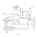
- Fig. 2 is a schematic structural diagram of an example of a charging apparatus based on a first embodiment of the invention.
- the charging apparatus 2 configured to charge a battery 100 includes a charging execution circuit 11, a charging protection circuit 12 and a charging control circuit 23.
- the charging control circuit 23 is configured to control the charging execution circuit 11 to adjust output voltage Vout and output current Iout generated at a charging output terminal thereof and to control charging by the charging execution circuit 11 to be terminated.
- the charging control circuit 23 in the charging apparatus 2 in the present embodiment includes a current adjustment module 231 and a detection control module 230.
- the current adjustment module 231 is configured to adjust an externally input nominal current reference Iref_s and to output a variable current reference Iref_g as a result of adjustment to a current reference input terminal of the charging execution circuit 11 (i.e., the negative input terminal of the differential amplifier 111) to control the charging execution circuit 11 to adjust the output voltage Vout and the output current Iout, where the lowest current value of the variable current reference Iref_g is lower than the nominal current reference Iref_s, and the highest current value of the variable current reference Iref_g is equal to the nominal current reference Iref_s; and
- the detection control module 230 is configured to trigger periodically interruption of charging, to control the current adjustment module 231 and to generate a charging termination signal Fin_b, where the variable current reference Iref_g is limited at the lowest current value above by controlling the current adjustment module 231 in a period of interruption, and the limitation above of the variable current reference Iref_g is removed by controlling the current adjustment module 231 in the period of charging spaced by periods of interruption; and when the output voltage Vout lower than an externally input nominal voltage reference Vref_s by a voltage difference lower than a preset voltage threshold Th_v1 (which approximately indicates that the kernel voltage V0 of the battery 100 has nearly reached the nominal voltage reference Vref_s) is detected at the end of the period of interruption, to set the charging termination signal Fin_b active to trigger termination of charging.
- Th_v1 which approximately indicates that the kernel voltage V0 of the battery 100 has nearly reached the nominal voltage reference Vref_s
- the lowest current value of the variable current reference Iref_g can be set by presetting an allowable difference range and setting the lowest current value on such a constraint condition that the difference of the output voltage Vout from the kernel voltage V0 of the battery (i.e., the voltage drop across the inner resistor R0 of the battery 100) is ensured to be in the allowable difference range.
- the size of the preset allowable difference range may vary with different specifications, and correspondingly a particular value of the lowest current value will vary; and moreover a particular value of the lowest current value will also vary correspondingly for a different characteristic of the PMOS 114 or an alternative device with an adjustable switch function in place of the PMOS 114 even if the size of the preset allowable difference range is determined.
- those skilled in the art with the knowledge of the function above of the lowest current value can determine a particular value of the lowest current value applicable to respective scenarios, so a detailed description thereof will be omitted here.
- variable current reference Ires_g is adjusted to the highest current value (i.e., the nominal current reference Iref_s) and maintained stably at the highest current value for the period of charging, or the variable current reference Iref_g is adjusted to a pre-selected default current value higher than the lowest current value and lower than or equal to the highest current value and maintained stably at the default current value for the period of charging, so a detailed description thereof will be omitted here.
- the current reference input terminal of the charging execution circuit 11 receives the variable current reference Iref_g instead of the constant nominal current reference Iref_s; and moreover in the present embodiment, the voltage reference input terminal of the charging execution circuit 11 (i.e., the negative input terminal of the differential amplifier 112) still receives the input nominal voltage reference Vref_s.
- variable current reference Iref_g will be limited to the lowest current value above in each period of interruption, the output current Iout will be higher and even far higher than the variable current reference Iref_g suddenly changed to the lowest current value each time the period of interruption commences; and correspondingly no matter whether the output voltage Vout at this time has not reached the nominal voltage reference Vref_s or has reached or been slightly higher than the nominal voltage reference Vref_s, the positive voltage value of the control signal Ctrl_I will be higher than the positive voltage value of the control signal Ctrl_V and control the PMOS 114 (i.e., the adjustable switch) to be turned off or weakly conductive so that the output current Iout will be dropped to be substantially equal to the variable current reference Iref_g limited at the lowest current value.
- the PMOS 114 i.e., the adjustable switch
- the PMOS 114 is still controlled by the control signal Ctrl_I and maintained turned off or weakly conductive;
- the voltage difference above detected at the end of the period of interruption in the present embodiment can approximately reflect whether the battery 100 has been charged fully, and correspondingly whether to trigger termination of charging can be judged more accurately by the voltage difference above, and consequently the drawback of insufficient charging can be alleviated, in the present embodiment as compared with the prior art in which termination of charging is triggered on the condition of the sufficient output current Iout.
- the voltage reference input terminal of the charging execution circuit 11 i.e., the negative input terminal of the differential amplifier 112 receives the nominal voltage reference Vref_s in the present embodiment
- those skilled in the art can appreciate from the following description of a third apparatus embodiment and a fourth apparatus embodiment that there will be no substantial influence upon the alleviation of the drawback of sufficient charging no matter whether the nominal voltage reference Vref_s is input at the voltage reference input terminal of the charging execution circuit 11.
- Fig. 3 is a schematic structural diagram of a preferred current adjustment module included in the charging control circuit in the charging apparatus based on the first embodiment of the invention.
- the current adjustment module 231 embodied in a variable-gain current mirror structure includes 2m adjustment shifts, and the current adjustment module 231 includes a current mirror trunk 2311, m current mirror branches 2312-1 to 2312-m and a m-bit decoder 2313, where m represents a positive integer higher than or equal to 1.
- the current mirror trunk 2311 includes an NMOS0.
- the drain D of the NMOS0 is the input terminal of the current mirror trunk 2311 and connected with the input terminal of the current adjustment module 231 to receive the nominal current reference Iref_s;
- the source S of the NMOS0 is the output terminal of the current mirror trunk 2311 and grounded;
- the gate G of the NMOS0 is connected with the drain D of the NMOS0 and pulled high so that the gate-source difference in voltage VGS between the gate G and the source S is at a positive value and higher than the cutoff voltage of the NMOS0, that is, the NMOS0 is normally-on, so the nominal current reference Iref_s received at the input terminal of the current mirror trunk 2311 from the input terminal of the current adjustment module 231 can be output at the output terminal of the current mirror trunk 2311.
- each current mirror branch 2312-i (where i represents a positive integer higher than or equal to 1 and lower than or equal to m) includes three NMOSi0 to NMOSi2 and an inverter Revi, where:
- the source S of the NMOSi0 is the input terminal of the current mirror branch 2312-i, and the drain D thereof is the output terminal of the current mirror branch 2312-i;
- the source S of the NMOSi1 is connected with the gate G of the NMOSi0, the drain D thereof is connected with the drain D of the NMOSi0 (pulled high), and the gate G thereof is connected with the i-th bit output terminal of the decoder 2313;
- the source S of the NMOSi2 is connected with the source S of the NMOS0 (grounded), the drain D thereof is connected with the gate G of the NMOSi0, and the gate G thereof is connected with the i-th bit output terminal of the decoder 2313 through the inverter Revi.
- the decoder 2313 receives a current encoded signal Icode at the input terminal thereof from the detection control module 230 over a current control bus and controls level statues of the m output terminals thereof by the current encoded signal Icode.
- the gate G of the NMOSi1 is pulled high to turn on the NMOSi1, and the gate G of the NMOSi2 is inverted by the inverter Revi and then pulled low to turn off the NMOSi2; and the turned-on NMOSi1 will further result in conductivity between the gate G of the NMOSi0 with the gate G of the NMOS0 so that a current mirror with a proportion of 1/m to the current mirror trunk 2311 is formed at the current mirror branch 2312-i, and consequently 1/m of the nominal current reference Iref_s is aggregated at the output terminal of the current adjustment module 231 through the output terminal of the current mirror branch 2312-i.
- the gate G of the NMOSi2 is pulled low to turn off the NMOSi1, and the gate G of the NMOSi2 is inverted by the inverter Revi and then pulled high to turn on the NMOSi2; and the turned-on NMOSi2 will further pull low the gate of the NMOSi0 to turn off NMOSi0 so that 1/m of the nominal current reference Iref_s received at the input terminal of the current mirror branch 2312-i will not be aggregated at the output terminal of the current adjustment module 231.
- the current adjustment module 231 can alternatively be embodied in another structure, e.g., a rheostat-based structure, so a repeated description thereof will be omitted here.
- the current adjustment module 231 can alternatively be controlled in another form of signal than the current encoded signal Icode.
- Fig. 4 is a schematic structural diagram of a preferred detection control module included in the charging control circuit in the charging apparatus based on the first embodiment of the invention.
- the detection control module includes a clock counter 2301, a logic controller 2302, a current counter 2304 and a voltage detector 2305.
- the clock counter 2301 is configured to count the reference clock signal CLK and to generate an interruption clock signal CLK_t from a result of counting, where the active interruption clock signal CLK_t indicates the period of interruption, and the inactive interruption clock signal CLK_t indicates the period of charging.
- the logic controller 2302 is configured to generate a current reset signal I_res from the interruption clock signal CLK_t, where the current reset signal I_res is set active at the active interruption clock signal CLK_t
- the current counter 2304 is configured to perform a counting operation based on the reference clock signal and the current reset signal I_res and to output a result of current counting to the current adjustment module 231 for adjustment by the current adjustment module 231 based on the result of current counting (with the current adjustment module 231 in the preferred structure as illustrated in Fig. 3 , the result of current counting can be output to the current adjustment module 231 in the form of the current encoded signal Icode for reception at the input terminal of the decoder 2313);
- a counting operation to increase the result of current counting by a current adjustment step size is performed once until the highest current counting value or a preset default current counting value is reached, where the highest current counting value corresponds to the highest current value of the variable current reference Iref_g (i.e., the nominal current reference Iref_s), and the default current counting value corresponds to the pre-selected default current value mentioned above, that is, in order that "the limitation above of the variable current reference Iref_g is removed", this is performed by the current counter 2304 through constantly counting to adjust rapidly the variable current reference Iref_g to the highest current value and maintaining it stably at the highest current value for the period of charging or through adjusting the variable current reference Iref_g to a pre-selected default current value higher than the lowest current value and lower than or equal to the highest current value and maintaining it stably at the default current value for the period of charging.
- the voltage detector 2305 is configured to detect the magnitude of a voltage difference by which the output voltage Vout is lower than the nominal voltage reference Vref_s and to generate a voltage detection signal V_t1 based on the magnitude of the voltage difference, where the voltage detection signal V_t1 is active when the voltage difference is lower than the voltage threshold Th_v1, that is, the active voltage detection signal V_t1 indicates that the output voltage Vout has nearly reached the nominal voltage reference Vref_s.
- the logic controller 2302 is further configured to generate the charging termination signal Fin_b from the interruption clock signal CLK_t and the voltage detection signal V_t1, where when the interruption clock signal CLK_t jumps from being active to an arriving inactive clock edge, if the voltage detection signal V_t1 is active (which approximately indicates at the end of the period of interruption that the kernel voltage V0 of the battery 100 has nearly reached the nominal voltage reference Vref_s), then the charging termination signal Fin_b is set active.
- the detection control module 230 can perform its corresponding function in the preferred structure above, where the clock counter 2301 and the current counter 2304 essentially perform the function of a counter well known to those skilled in the art, so a repeated description of implementations of the clock counter 2301 and the current counter 2304 will be omitted here; and although a number of implementations of the voltage detector 2305 and the logic controller 2302 can be embodied by those skilled in the art in combinations of various elements, they will be further described below respectively by way of an example.
- the voltage detector 2305 detecting the magnitude of a voltage difference by which the output voltage Vout is lower than the nominal voltage reference Vref_s substantially detects the closeness of the output voltage Vout to the nominal voltage reference Vref_s. Then in a particular implementation, firstly the particular voltage value of the voltage difference can be detected and then the particular voltage value of the voltage difference can be compared with the voltage threshold Th_v1, or firstly a voltage difference equivalent to a loss by the voltage threshold Th_v1 can be extracted from the nominal voltage reference Vref_s and then the output voltage Vout can be compared with the extracted voltage difference.
- Fig. 5 is a schematic diagram of a particular example of the voltage detector in the detection control module illustrated in Fig. 4 .
- a voltage difference equivalent to a loss by the voltage threshold Th_v1 can be extracted from the nominal voltage reference Vref_s and then the output voltage Vout can be compared with the voltage difference in Fig. 5 .
- the voltage detector 2305 includes a comparator Comp_vt1, where the negative input terminal of the comparator Comp_vt1 receives the output voltage Vout, the other positive input terminal of the comparator Comp_vt1 receives the voltage difference Vref_s-Th_v1 between the nominal voltage reference Vref_s and the voltage threshold Th_v1, and the output terminal of the comparator Comp_vt1 generates the voltage detection signal V_t1, where:
- the logic controller 2302 generally performs a logic judgment and trigger function.
- Fig. 6 is a schematic diagram of a particular example of the logic controller in the detection control module illustrated in Fig. 4 .
- a logic judgment and trigger scheme easy to implement is adopted in Fig. 6 .
- the logic controller 2302 includes inverters Rev_c1 and Rev_c2, a resistor Rf, a capacitor Cf, a D flip-flop DFF 1 and an inverter Rev_v1.
- the reference clock signal CLK_t is inverted by the inverter Rev_c1, delayed by a delay circuit consisted of the resistor Rf and the capacitor Cf and inverted by the inverter Rev_c2 in that order to generate the current reset signal I_res so that when the reference clock signal CLK_t is active at a high level indicating a period of interruption, the current reset signal I_res is set active at a high level and slightly delayed from the reference clock signal CLK_t, and when the reference clock signal CLK_t is inactive at a low level indicating the period of charging, the current reset signal I_res is set inactive at a low level and slightly delayed from the reference clock signal CLK_t.
- the D flip-flop DFF1 is controlled by the reference clock signal CLK inverted by the inverter Rev_c1 and triggers inversion of the level status of the charging termination signal Fin_b based on the level status of the voltage detection signal V_t1 inverted by the inverter Rev_v1 so that the charging termination signal Fin_b is inverted from being inactive at a low level to being active at a high level based on the active voltage detection signal V_t1 at a low level at the rising edge of the inverted reference clock signal CLK_t, that is, when the reference clock signal CLK_t jumps from being active at a high level to an arriving falling edge inactive at a low level (at the end of the period of interruption).
- Fig. 7 is a schematic structural diagram of an example of a charging apparatus based on a second embodiment of the invention.
- the charging apparatus 3 configured to charge a battery 100 includes a charging execution circuit 11, a charging protection circuit 12 and a charging control circuit 33.
- the charging control circuit 33 is configured to control the charging execution circuit 11 to adjust output voltage Vout and output current Iout generated at a charging output terminal thereof and to control charging by the charging execution circuit 11 to be terminated.
- the charging control circuit 33 in the charging apparatus 3 in the present embodiment includes the current adjustment module 231 and a detection control module 330.
- the detection control module 330 is configured to trigger periodically interruption of charging, to control the current adjustment module 231 and to generate a charging termination signal Fin_b, where the variable current reference Iref_g is limited at the lowest current value above by controlling the current adjustment module 231 in a period of interruption, and the limitation above of the variable current reference Iref_g is removed by controlling the current adjustment module 231 in the period of charging spaced by periods of interruption; and when the output voltage Vout lower than an externally input nominal voltage reference Vref_s by a voltage difference lower than the preset voltage threshold Th_v1 (which approximately indicates that the kernel voltage V0 of the battery 100 has nearly reached the nominal voltage reference Vref_s) is detected at the end of the period of interruption, to set the charging termination signal Fin_b active to trigger termination of charging; and
- variable current reference Iref_g with the limitation thereof above being removed has the following several varying status dependent upon the control of the current adjustment module 231 by the detection control module 330:
- variable current reference Iref_g When the output current Iout lower than the variable current reference Iref_g by a current difference lower than a preset current threshold Th_i1 (which indicates that the output current Iout has been very close to the current variable current reference Iref_g) is detected in the period of charging, if the variable current reference Iref_g has not reached the highest current value thereof (i.e., the nominal current reference Iref_s), then the variable current reference Iref_g is adjusted up by the current adjustment module 231;
- variable current reference Iref_g When the output current Iout lower than the variable current reference Iref_g by a current difference higher than or equal to a preset current threshold Th_i2 and lower than a preset current threshold Th_i3 (which indicates that the output current Iout has been significantly lower than the current variable current reference Iref_g) is detected in the period of charging, if the variable current reference Iref_g has not reached the lowest current value above, then the variable current reference Iref_g is adjusted down by the current adjustment module 231; and
- variable current reference Iref_g When the output current Iout lower than the variable current reference Iref_g by a current difference higher than or equal to the preset current threshold Th_i3 (which indicates that the output current Iout has been far lower than the current variable current reference Iref_g) is detected in the period of charging, if the variable current reference Iref_g has not reached the lowest current value above, then the variable current reference Iref_g is reset to the lowest current value above by the current adjustment module 231; and
- the current reference input terminal of the charging execution circuit 11 receives the variable current reference Iref_g instead of the constant nominal current reference Iref_s; and moreover in the present embodiment, the voltage reference input terminal of the charging execution circuit 11 (i.e., the negative input terminal of the differential amplifier 112) still receives the input nominal voltage reference Vref_s.
- variable current reference Iref_g will be limited to the lowest current value above in each period of interruption, the drawback of insufficient charging can be alleviated in the present embodiment as in the first apparatus embodiment.
- variable current reference Iref_g can be adjusted adaptively to the varying output current Iout in the period of charging in the present embodiment, that is, the present embodiment can be implemented simply by adjusting the variable current reference Iref_g adaptively so that "the limitation above of the variable current reference Iref_g is removed" as described in the first embodiment.
- the lower output current Iout is accommodated by lowering the variable current reference Iref_g to thereby avoid an instantaneous up-rush of the rebounding output current Iout;
- the instantaneously suddenly dropped output current Iout upon sudden fluctuation is accommodated by resetting the variable current reference Iref_g to the lowest current value above to thereby avoid an instantaneous up-rush of the rebounding output current Iout with an instantaneous sudden raise due to sudden fluctuation.
- an instantaneous up-rush of the output current Iout can be further refrained by adjusting the variable current reference Iref_g in the period of charging in the present embodiment as compared with the first apparatus embodiment.
- the detection control module 330 can be further configured to have the variable current reference Iref_g reset to the lowest current value above by controlling the current adjustment module 231 when the charging termination signal Fin_b is set active to thereby avoid an instantaneous up-rush of the output current Iout at the beginning of the next time of charging.
- the voltage reference input terminal of the charging execution circuit 11 i.e., the negative input terminal of the differential amplifier 112 receives the nominal voltage reference Vref_s in the present embodiment
- the nominal voltage reference Vref_s receives the nominal voltage reference Vref_s in the present embodiment
- Fig. 8 is a schematic structural diagram of a preferred detection control module included in the charging control circuit in the charging apparatus based on the second embodiment of the invention.
- the detection control module 330 includes the clock counter 2301, a logic controller 3302, a current detector 3303, a current counter 3304 and the voltage detector 2305.
- the clock counter 2301 has been described in the first apparatus embodiment, so a repeated description thereof will be omitted in the present embodiment.
- the logic controller 3302 periodically triggers interruption of charging based on the interruption clock signal CLK_t generated by the clock counter 2301 in the same way as the logic controller 2302 in the first apparatus embodiment, so a repeated description thereof will also be omitted in the present embodiment.
- the current detector 3303 is configured to detect the magnitude of a current difference by which the output current Iout is lower than the variable current reference Iref_g and to generate a current detection signal I_t1, a current detection signal I_t2 and a current detection signal I_t3 based on the magnitude of the current difference, where the current detection signal I_t1 is active when the current difference above is lower than the current threshold Th_i1, the current detection signal I_t2 is active when the current difference above is lower than the current threshold Th_i2, and the current detection signal I_t3 is active when the current difference above is lower than the current threshold Th_i3.
- Table 1 I_t1 I_t2 I_t3 Range including ⁇ I Definition Active Active Active ⁇ I ⁇ Th_i1 Iout very close Iref_g Inactive Active Active Th_i1 ⁇ I ⁇ Th_i2 Appropriate difference of Iout from Iref_9 Inactive Inactive Active Th_i2 ⁇ I ⁇ Th_i3 Iout significantly lower than Iref_g Inactive Inactive Inactive Th_i3 ⁇ I Iout far lower than Iref_g
- ⁇ I represents a current difference by which the output current Iout is lower than the variable current reference Iref_g.
- the logic controller 2302 is configured to generate a current-up signal I_up, a current-down signal I_down and a current reset signal I_res based on the interruption clock signal CLK_t generated by the clock counter 2301 and the current detection signals I_t1 to I_t3 generated by the current detector 3303, where with the definitions of the various combinations of levels depicted in Table 1, the current-up signal I_up, the current-down signal I_down and the current reset signal I_res generated by the logic controller 2302 vary in level as follow:
- the current reset signal I_res is set inactive.
- the current counter 3304 is configured to perform a counting operation based on the reference clock signal CLK_s, the current-up signal I_up, the current-down signal I_down and the current reset signal I_res and to output a result of current counting to the current adjustment module 231 for adjustment by the current adjustment module 231 based on the result of current counting (with the current adjustment module 231 in the preferred structure as illustrated in Fig. 3 , the result of current counting can be output to the current adjustment module 231 in the form of a current encoded signal Icode for reception at the input terminal of the decoder 2313), where each time the reference clock signal CLK_s jumps from being inactive to an arriving active clock edge:
- the respective current adjustment step sizes can be set uniformly, that is, the numbers of adjustment shifts corresponding to the respective current adjustment step sizes can be set uniformly; or of course the current adjustment step sizes may not be set uniformly, that is, each current adjustment step size can be set by increasing or decreasing a preceding or succeeding current adjustment step size by at least one adjustment shift);
- the voltage detector 2305 has been described in the first apparatus embodiment, so a repeated description thereof will be omitted in the present embodiment.
- the logic controller 3302 generates the charging termination signal Fin_b based on the interruption clock signal CLK_t generated by the clock counter 2301 and the voltage detection signal V_t1 generated by the voltage detector 2305 in the same way as the logic controller 2302 in the first apparatus embodiment, so a repeated description thereof will also be omitted in the present embodiment.
- the logic controller 3302 can further reset the current reset signal I_res active when the charging termination signal Fin_b is active.
- the current reset signal I_res is set inactive at a low level when the current detection signal I_t3 is inactive, the charging termination signal Fin_b is inactive and the delayed reference clock signal CLK_t' is inactive indicating the period of charging.
- the detection control module 330 can perform its corresponding function in the preferred structure above, where the current counter 3304 essentially perform the function of a counter well known to those skilled in the art, so a repeated description of an implementation of the current counter 3304 will be omitted here; and although a number of implementations of the current detector 3303 and the logic controller 3302 can be embodied by those skilled in the art in combinations of various elements, they will be further described below respectively by way of an example.
- the current can be converted into corresponding voltage for comparison for the sake of an easier implementation of whichever detection scheme above in use.
- Fig. 9 is a schematic diagram of a particular example of the current detector in the detection control module illustrated in Fig. 8 .
- voltage differences equivalent respectively to losses by the current thresholds Th_i1 to TH_i3 can be extracted from the current variable current reference Iref_g and then the output current Iout can be compared respectively with the respective extracted current differences by converting the output current Iout and the respective current differences into corresponding voltage for comparison in Fig. 9 .
- the current counter 3304 includes resistors Ra, Rb, Rc, Rd and Rout and also comparators Comp_it1 to Comp_it3.
- the resistors Ra, Rb, Rc and Rd are connected in series into a string of resistors, where the terminal of the string of resistors at the resistor Ra side receives the variable current reference Iref_g, and the other terminal thereof at the resistor Rd is grounded.
- the terminal of the string of resistors at the resistor Ra side can generate voltage corresponding in magnitude to the variable current reference Iref_g; and there are increasing voltage drops across the connected terminals of the resistors Ra and Rb, the connected terminals of the resistors Rb and Rc and the connected terminals of the resistors Rc and Rd in that order, and the increasing voltage drops correspond in magnitude respectively to the current thresholds Th_i1 to Th_i3.
- the voltages across the connected terminals of the resistors Ra and Rb, the connected terminals of the resistors Rb and Rc and the connected terminals of the resistors Rc and Rd correspond in magnitude respectively to the current differences in the variable current reference Iref_g equivalent to losses by the current thresholds Th_i1 to Th_i3.
- One terminal of the resistor Rout receives the output current Iout, and the other terminal thereof is grounded.
- the terminal of the resistor Rout at which the output current Iout is received can generate voltage corresponding in magnitude to the output current Iout.
- the negative input terminal of the comparator Comp_it1 is connected with the terminal of the Rout at which the output voltage Vout is received, and the other positive input terminal thereof is connected with the connected terminals of the Ra and the Rb, and the output terminal of the comparator Comp_it1 generates the current detection signal I_t1, where when the voltage at the terminal of the Rout at which the output voltage Vout is received is lower than or equal to the voltage at the connected terminals of the Ra and the Rb, this indicates that a current difference by which the output current Iout is lower than the variable current reference Iref_g is higher than or equal to the current threshold Th_il, so the current detection signal I_t1 at this time is inactive at a high level; and when the voltage at the terminal of the Rout at which the output voltage Vout is received is higher than the voltage at the connected terminals of the Ra and the Rb, this indicates that a current difference by which the output current Iout is lower than the variable current reference Iref_g is lower than the current threshold Th_i1, so the current detection
- the negative input terminal of the comparator Comp_it2 is connected with the terminal of the Rout at which the output voltage Vout is received, and the other positive input terminal thereof is connected with the connected terminals of the Rb and the Rc, and the output terminal of the comparator Comp_it2 generates the current detection signal I_t2 under the same principle as the comparator Comp_it1;
- the negative input terminal of the comparator Comp_it3 is connected with the terminal of the Rout at which the output voltage Vout is received, and the other positive input terminal thereof is connected with the connected terminals of the Rc and the Rd, and the output terminal of the comparator Comp_it3 generates the current detection signal I_t3 under the same principle as the comparator Comp_it1.
- the logic controller 3302 generally performs a logic judgment and trigger function.
- Fig. 10 is a schematic diagram of a particular example of the logic controller in the detection control module illustrated in Fig. 8 .
- a logic judgment and trigger scheme easy to implement is adopted in Fig. 10 .
- the logic controller 2302 includes inverters Rev_i1 and Rev_i2, an AND gate ANDi and an OR gate OR and also Rev_c1 and Rev_c2, a resistor Rf, a capacitor Cf, a D flip-flop DFF and an inverter Rev_v1.
- the current detection signal I_t1 is inverted by the inverter Rev_i1 to thereby generate the current-up signal I_up; and if the current detection signal I_t1 is active at a low level, then the current-up signal I_up becomes active at a high level; otherwise, the current-up signal I_up becomes inactive at a low level.
- the current detection signal I_t2 is input to the AND gate ANDi, and the current detection signal I_t3 is inverted by the inverter Rev_i2 and also input to the AND gate ANDi; and when the current detection signal I_t2 is inactive at a high level and the current detection signal I_t3 is active at a low level, the current-down signal I_down output by the AND gate ANDi becomes active at a high level; otherwise, the current-down signal I_down output by the AND gate ANDi becomes inactive at a low level.
- the current detection signal I_t3 is output to the OR gate OR; and when the current detection signal I_t3 is inactive at a high level, the current rest signal I_res output by the OR gate OR becomes active at a high level.
- the reference clock signal CLK_t is inverted by the inverter Rev_c1, delayed by a delay circuit consisted of the resistor Rf and the capacitor Cf and inverted by the inverter Rev_c2 in that order and then delayed to generate the reference clock signal CLK_t' output to the OR gate OR, and when the delayed reference clock signal CLK_t' is active at a high level indicating a period of interruption, the current reset signal I_res output by the OR gate OR becomes active at a high level.
- the D flip-flop DFF1 is controlled by the reference clock signal CLK_t inverted by the inverter Rev_c1 and triggers inversion of the level status of the charging termination signal Fin_b based on the level status of the voltage detection signal V_t1 inverted by the inverter Rev_v1 so that the charging termination signal Fin_b is inverted from being inactive at a low level to being active at a high level based on the active voltage detection signal V_t1 at a low level at the rising edge of the inverted reference clock signal CLK_t, that is, when the reference clock signal CLK_t jumps from being active at a high level to an arriving falling edge inactive at a low level (at the end of the period of interruption).
- the detection control module 330 if it is necessary for the detection control module 330 to further have the variable current reference Iref_g reset to the lowest current value above by controlling the current adjustment module 231 when the charging termination signal Fin_b is set active, then the charging termination signal Fin_b is output to the OR gate OR (represented by a dotted line in Fig. 10 ) in addition to the charging control circuit 33; and when the charging termination signal Fin_b is active at a high level, the current reset signal I_res output by the OR gate becomes active at a high level.
- Fig. 11 is a schematic waveform diagram of output current generated by the charging apparatus based on the second embodiment of the invention.
- the result of current counting represented by the current encoded signal Icode will gradually increase with the raising output current Iout or gradually increase with the dropping output current Iout at the frequency of the reference clock signal CLK_t in the period of charging using the solution of the present embodiment to thereby avoid an instantaneous up-rush of the output current Iout.
- Fig. 12 is a schematic structural diagram of an example of a charging apparatus based on a third embodiment of the invention.
- the charging apparatus 4 configured to charge a battery 100 includes a charging execution circuit 11, a charging protection circuit 12 and a charging control circuit 43.
- the charging control circuit 43 is configured to control the charging execution circuit 11 to adjust output voltage Vout and output current Iout generated at a charging output terminal thereof and to control charging by the charging execution circuit 11 to be terminated.
- the charging control circuit 43 in the charging apparatus 4 in the present embodiment includes the current adjustment module 231, a voltage adjustment module 432 and a detection control module 430.
- the voltage adjustment module 432 is configured to adjust the nominal voltage reference Vref_s and to output a variable voltage reference Vref_g as a result of adjustment to a voltage reference input terminal of the charging execution circuit 11 (i.e., the negative input terminal of the differential amplifier 112) to control the charging execution circuit 11 to adjust the output voltage Vout and the output current Iout, where the highest voltage value of the variable voltage reference Vref_g is higher than the nominal voltage reference Vref_s, and the lowest voltage value of the variable voltage reference Vref_g is equal to the nominal voltage reference Vref_s;
- the detection control module 430 is configured to trigger periodically interruption of charging, to control the current adjustment module 231 and to generate a charging termination signal Fin_b, where the variable current reference Iref_g is limited at the lowest current value above by controlling the current adjustment module 231 in a period of interruption, and the limitation above of the variable current reference Iref_g is removed by controlling the current adjustment module 231 in the period of charging spaced by periods of interruption; and when the output voltage Vout lower than an externally input nominal voltage reference Vref_s by a voltage difference lower than the voltage threshold Th_v1 (which approximately indicates that the kernel voltage V0 of the battery 100 has nearly reached the nominal voltage reference Vref_s) is detected at the end of the period of interruption, to set the charging termination signal Fin_b active to trigger termination of charging; and
- the detection control module 430 is further configured to control the voltage adjustment module 432, and the variable voltage reference Vref_g has the following several varying status dependent upon the control of the voltage adjustment module 432 by the detection control module 430:
- variable voltage reference Vref_g When the voltage difference above higher than a preset voltage threshold Th_v3 (which indicates the output voltage Vout at the end of the period of interruption has not reached the nominal voltage reference Vref_s) is detected at the end of the period of interruption, if the variable voltage reference Vref_g has not reached the highest voltage value above, then the variable voltage reference Vref_g is adjusted up by the voltage adjustment module 432;
- the current reference input terminal of the charging execution circuit 11 receives the variable current reference Iref_g instead of the constant nominal current reference Iref_s; and the variable voltage reference Vref_g instead of the constant nominal voltage reference Vref_s is input at the voltage reference input terminal of the charging execution circuit 11.
- variable current reference Iref_g will be limited to the lowest current value above in each period of interruption, the output current Iout will be higher and even far higher than the variable current reference Iref_g suddenly changed to the lowest current value each time the period of interruption commences; and correspondingly no matter whether the output voltage Vout at this time has not reached the variable voltage reference Vref_g or has reached or been slightly higher than the variable voltage reference Vref_g, the positive voltage value of the control signal Ctrl_I will be higher than the positive voltage value of the control signal Ctrl-V and control the PMOS 114 (i.e., the adjustable switch) to be turned off or weakly conductive so that the output current Iout will be dropped to be substantially equal to the variable current reference Iref_g limited at the lowest current value.
- the PMOS 114 i.e., the adjustable switch
- the PMOS 114 is still controller by the control signal Ctrl_I and maintained turned off or weakly conductive;
- the nominal voltage reference Vref_s received at the reference voltage input terminal of the charging execution circuit 11 is replaced with the variable voltage reference Vref_g in the present embodiment as opposed to the first apparatus embodiment, after the output current Iout is substantially equal to the variable current reference Iref_g limited at the lowest current value, the status of being substantially equal can still be guaranteed for the period of interruption in the present embodiment as in the first apparatus embodiment.
- variable voltage reference Vref_g can be adjusted adaptively to the closeness of the output voltage Vout (approximately the kernel voltage V0 of the battery 100) to the nominal voltage reference Vref_s each time the period of interruption ends in the present embodiment so that:
- charging can further be speeded up by adjusting the variable voltage reference Vref_g at the end of the period of interruption in the present embodiment as compared with the first apparatus embodiment and the second apparatus embodiment.
- the detection control module 430 can be further configured to have the variable voltage reference Vref_g reset to the lowest current value above by controlling the voltage adjustment module 432 when the charging termination signal Fin_b is set active.
- Fig. 13 is a schematic structural diagram of a preferred voltage adjustment module included in the charging control circuit in the charging apparatus based on the third embodiment of the invention.
- the voltage adjustment module 432 includes a resistance-adjustable circuit 4321 with n shifts and an n-bit decoder 4322, where n represents a positive integer higher than 2.
- the resistance-adjustable circuit 4321 includes resistors R1 to Rn and NMOS1 to NMOSn.
- the resistors R1 to Rn are connected in series into a string of resistors, where the terminal of the string of resistors at the resistor R1 receives the nominal voltage reference Vref_s, and the other terminal of the string of resistors at the resistor Rn is connected with a power source Vccl and configured to generate the variable voltage reference Vref_g.
- the source S of the NMOS1 is connected with the terminal of the string of resistors at which the nominal voltage reference Vref_s is received, the drain D thereof is connected with the other terminal of the string of resistors at the resistor Rn (that is, connected with the power source Vcc1), and the gate G thereof is connected with the first bit output terminal of the decoder 4322; and
- the source S of the NMOSj is connected with the terminal of the resistor Rj connected with the resistor Rj-1, the drain D thereof is connected with the other terminal of the string of resistors at the resistor Rn (that is, connected with the power source Vcc1), and the gate G thereof is connected with the j-th bit output terminal of the decoder 4322, where j represents a positive integer higher than and lower than or equal to n.
- the decoder 4322 receives a voltage encoded signal Vcode at the input terminal thereof from the detection control module 430 over a voltage control bus and controls level statues of the n output terminals thereof by the voltage encoded signal Vcode.
- the NMOS 1 When the first bit output terminal of the decoder 4322 is at a high level, the NMOS 1 is turned off and when the first bit output terminal of the decoder 4322 is at a low level, the NMOS1 is turned on to short all the resistors R1 to Rn so that the variable voltage reference Vref_g is equal to the nominal voltage reference Vref_s, i.e., the lowest voltage value above;
- the NMOSj When the j-th bit output terminal of the decoder 4322 is at a high level, the NMOSj is turned off; and when the j-th bit output terminal of the decoder 4322 is at a low level, the NMOSj is turned on to short the resistors Rj to Rn so that there is some increment of the variable voltage reference Vref_g from the nominal voltage reference Vref_s due to the un-shorted resistors R1 to Rj-1 in the case that the NMOS1 to NMOSj are turned off; and
- variable voltage reference Vref_g has the largest increment from the nominal voltage reference Vref_s, that is, reaches the highest voltage value above, due to the un-shorted resistors R1 to Rn.
- the different adjustment shifts can be available by shorting different numbers of resistors among the resistors R1 to Rn in the preferred structure as illustrated in Fig. 13 .
- the uniformity or non-uniformity of the respective adjustment shifts can be achieved by setting the resistances of the resistors R1 to Rn.
- the voltage adjustment module 432 can alternatively be embodied in another structure, for example, a number of voltage values higher than or equal to the nominal voltage reference Vref_s are provided concurrently based upon the nominal voltage reference Vref_s, and one of the voltage values is selected by the decoder 4322 as the variable voltage reference Vref_g.
- the voltage adjustment module 432 can alternatively be controlled in another form of signal than the voltage encoded signal Vcode.
- Fig. 14 is a schematic structural diagram of a preferred detection control module included in the charging control circuit in the charging apparatus based on the third embodiment of the invention.
- the detection control module 430 includes the clock counter 2301, a logic controller 4302, the current detector 2304, a voltage detector 4305 and a voltage counter 4306.
- the clock counter 2301 has been described in the first apparatus embodiment, so a repeated description thereof will be omitted in the present embodiment.
- the logic controller 4302 periodically triggers interruption of charging based on the interruption clock signal CLK_t generated by the clock counter 2301 in the same way as the logic controller 2302 in the first apparatus embodiment, so a repeated description thereof will also be omitted in the present embodiment.
- the current detector 2304 has been described in the first apparatus embodiment, so a repeated description thereof will be omitted in the present embodiment.
- the logic controller 4302 controls the current detector 2304 by the current reset signal I_res in the same way as the logic controller 2302 in the first apparatus embodiment, so a repeated description thereof will also be omitted in the present embodiment.
- the voltage detector 4305 is configured to detect the magnitude of a voltage difference by which the output voltage Vout is lower than the variable voltage reference Vref_g and to generate a voltage detection signal V_t1, a voltage detection signal V_t2 and a voltage detection signal V_t3 based on the magnitude of the voltage difference, where the voltage detection signal V_t1 is active when the voltage difference above is lower than the voltage threshold Th_V1, the voltage detection signal V_t2 is active when the voltage difference above is lower than the voltage threshold Th_V2, and the voltage detection signal V_t3 is active when the voltage difference above is lower than the voltage threshold Th_V3.
- V_t1 V_t2 V_t3 Range including ⁇ V Definition Active Active Active ⁇ V ⁇ Th_V1 Vout at the end of the period of interruption (nearly equal to V0) has nearly reached Vref_g Inactive Active Active Th_V1 ⁇ V ⁇ Th_V2 Vout at the end of the period of interruption (nearly equal to V0) will nearly reach Vref_g Inactive Inactive Active Th_V2 ⁇ V ⁇ Th_V3
- Vout at the end of the period of interruption (nearly equal to V0) from Vref_g Inactive Inactive Inactive Th_V3 ⁇ V Vout at the end of the period of interruption (nearly equal to V0) has been far from reaching Vref_g
- ⁇ V represents a voltage difference by which the output voltage Vout is lower than the variable voltage reference Vref_g.
- the logic controller 4302 is configured to generate an adjustment clock signal CLK_g based on the interruption clock signal CLK_t generated by the clock counter 2301 and to generate the charging termination signal Fin_b, a voltage-down signal V_down and a voltage-up signal V_up based on the interruption clock signal CLK_t and the voltage detection signals V_t1 to V_t3 generated by the voltage detector 4305, where the adjustment clock signal CLK_g is the inverted interruption clock signal CLK_t; and with the definitions of the various combinations of levels depicted in Table 2, the charging termination signal Fin_b, the voltage-down signal V_down and the voltage-up signal V_up generated by the logic controller 4302 vary in level as follow:
- the voltage counter 4306 is configured to perform a counting operation based on the adjustment clock signal CLK_g, the voltage-up signal V_up and the voltage-down signal V_down and to output a result of voltage counting to the voltage adjustment module 432 for adjustment by the voltage adjustment module 432 based on the result of voltage counting (with the voltage adjustment module 432 in the preferred structure as illustrated in Fig. 13 , the result of voltage counting can be output to the voltage adjustment module 432 in the form of a voltage encoded signal Vcode for reception at the input terminal of the decoder 4311), where each time the adjustment clock signal CLK_g jumps from being inactive to an arriving active clock edge (at the beginning of the period of interruption):
- the respective voltage adjustment step sizes can be set uniformly, that is, both the adjustment amplitudes of the respective adjustment shifts and the numbers of adjustment shifts corresponding to the respective voltage adjustment step sizes can be set uniformly; or of course the voltage adjustment step sizes may not be set uniformly, that is, the adjustment amplitudes of the respective adjustment shifts may not be set uniformly and the numbers of adjustment shifts corresponding to the respective voltage adjustment step sizes can be set uniformly, or the adjustment amplitudes of the respective adjustment shifts can be set uniformly but each voltage adjustment step size can be set by increasing or decreasing a preceding or succeeding voltage adjustment step size by at least one adjustment shift); and
- the logic controller 4302 can further generate a voltage reset signal V_res from the charging termination signal Fin_b, where the voltage reset signal V_res is set active when the charging termination signal Fin_b is active, and the voltage reset signal V_res is set inactive when the charging termination signal Fin_b is inactive; and correspondingly the voltage counter 4306 is further configured to perform a counting operation based on the voltage reset signal V_res by performing a counting operation to reset the result of voltage counting to the lowest voltage counting value when the voltage reset signal V_res is active, where the lowest voltage counting value corresponds to the lowest voltage value above, i.e., the nominal voltage reference Vref_s.
- the detection control module 330 can perform its corresponding function in the preferred structure above, where the voltage counter 4306 essentially performs the function of a counter well known to those skilled in the art, so a repeated description of an implementation of the voltage counter 4306 will be omitted here; and although a number of implementations of the voltage detector 4305 and the logic controller 4302 can be embodied by those skilled in the art in combinations of various elements, they will be further described below respectively by way of an example.
- the voltage detector 4305 detecting the magnitude of a voltage difference by which the output voltage Vout is lower than the nominal voltage reference Vref_s substantially detects the closeness of the output voltage Vout to the nominal voltage reference Vref_s. Then in a particular implementation, firstly the particular voltage value of the voltage difference can be detected and then the particular voltage value of the voltage difference can be compared respectively with the voltage thresholds Th_v1 to Th_v3, or firstly voltage differences equivalent respectively to losses by the voltage thresholds Th_v1 to Th_v3 can be extracted from the nominal voltage reference Vref_s and then the output voltage Vout can be compared respectively with the respective extracted voltage differences.
- Fig. 15 is a schematic diagram of a particular example of the voltage detector in the detection control module illustrated in Fig. 14 .
- voltage differences equivalent respectively to losses by the voltage thresholds Th_v1 to Th_v3 can be extracted from the nominal voltage reference Vref_s and then the output voltage Vout can be compared respectively with the respective voltage differences in Fig. 15 .
- the voltage counter 4305 includes three comparators Comp_vt1 to Comp_vt3.
- the negative input terminal of the Comp_vt1 receives the output voltage Vout, and the other positive input terminal thereof receives the difference voltage Vref_s-Th_v1 between the nominal voltage reference Vref_s and the voltage threshold Th_v1, and the output terminal of the comparator Comp_vt1 generates the voltage detection signal V_t1, where:
- the negative input terminal of the Comp_vt2 receives the output voltage Vout, and the other positive input terminal thereof receives the difference voltage Vref_s-Th_v2 between the nominal voltage reference Vref_s and the voltage threshold Th_v2, and the output terminal of the comparator Comp_vt2 generates the voltage detection signal V_t2, where:
- the negative input terminal of the Comp_vt3 receives the output voltage Vout, and the other positive input terminal thereof receives the difference voltage Vref_s-Th_v3 between the nominal voltage reference Vref_s and the voltage threshold Th_v3, and the output terminal of the comparator Comp_vt3 generates the voltage detection signal V_t3, where:
- the logic controller 4302 generally performs a logic judgment and trigger function.
- Fig. 16 is a schematic diagram of a particular example of the logic controller in the detection control module illustrated in Fig. 14 .
- a logic judgment and trigger scheme easy to implement is adopted in Fig. 16 .
- the logic controller 4302 includes inverters Rev_c1 to Rev_c3, a resistor Rf, a capacitor Cf, D flip-flop DFF1 to DFF3, an AND gate AND_v, and inverters Rev_v1 and Rev_v2.
- the reference clock signal CLK_t is inverted by the inverter Rev_c1, delayed by a delay circuit consisted of the resistor Rf and the capacitor Cf and inverted by the inverter Rev_c2 in that order and then inverted by the inverter Rev_c3 to generate the adjustment clock signal CLK_g inverted at some delay from the reference clock signal CLK_t.
- the D flip-flop DFF2 is controller by the reference clock signal CLK_t inverted by the inverter Rev_c1 and triggers inversion of the level status of the voltage-down signal V_down based on a level status output by the AND gate AND_v, and one input terminal of the AND gate AND_v receives the voltage detection signal V_t1, and the other input terminal thereof receives the voltage detection signal V_t2 inverted by the inverter Rev_v2, so that the voltage-down signal V_down is inverted from being inactive at a low level to being active at a high level based on the voltage detection signal V_t1 inactive at a high level and the voltage detection signal V_t2 active at a low level at the rising edge of the inverted reference clock signal CLK_t, that is, when the reference clock signal CLK_t jumps from being active at a high level to an arriving falling edge inactive at a low level (at the end of the period of interruption).
- the D flip-flop DFF3 is controller by the inverted reference clock signal CLK_t inverted by the inverter Rev_c1 and triggers inversion of the level status of the voltage-up signal V_up based on the level status of the voltage detection signal V_t3 so that the voltage-up signal V_up is inverted from being inactive at a low level to being active at a high level based on the voltage detection signal V_t3 inactive at a high level at the rising edge of the inverted reference clock signal CLK_t, that is, when the reference clock signal CLK_t jumps from being active at a high level to an arriving falling edge inactive at a low level (at the end of the period of interruption).
- the charging termination signal Fin_b has the voltage reset signal V_res generated sequentially through the inverters Rev_v3 and Rev_v4 (represented by a dotted line in Fig. 16 ) in addition to being output to the charging control circuit 43; and when the charging termination signal Fin_b is active at a high level, the voltage reset signal V_res becomes active at a high level.
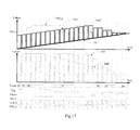
- Fig. 17 is a schematic waveform diagram of output voltage and corresponding output current generated by the charging apparatus based on the third embodiment of the invention.
- the output voltage Vout will return to the status of being substantially equal to the kernel voltage V0 of the battery 100 so that the result of voltage counting represented by the voltage encoded signal Vcode will gradually increase with the raising kernel voltage V0 detected by detecting the output voltage Vout each time the period of interruption ends, and thus the output voltage Vout higher than the nominal voltage reference Vref_s can be allowed so that the output current Iout will not become lower after the output voltage Vout reaches the nominal voltage reference Vref_s to thereby speed up charging.
- the output voltage Vout' in the period of charging without using the solution of the present embodiment, the output voltage Vout' must not be higher than the nominal voltage reference Vref_s so that the output current Iout' will start to become lower after the output voltage Vout' reaches the nominal voltage reference Vref_s to thereby slow down charging.
- the segment the waveform of the output current Iout above the waveform of the output current Iout' represents an increment in current due to speeded-up charging over the period after the output voltage Vout and Vout' reaches the nominal voltage reference Vref_s.
- Fig. 18 is a schematic structural diagram of an example of a charging apparatus based on a fourth embodiment of the invention.
- the charging apparatus 4 configured to charge a battery 100 includes a charging execution circuit 11, a charging protection circuit 12 and a charging control circuit 53.
- the charging control circuit 53 is configured to control the charging execution circuit 11 to adjust output voltage Vout and output current Iout generated at a charging output terminal thereof and to control charging by the charging execution circuit 11 to be terminated.
- the charging control circuit 53 in the charging apparatus 5 in the present embodiment includes the current adjustment module 231, the voltage adjustment module 432 and a detection control module 530.
- the detection control module 530 is configured to trigger periodically interruption of charging, to control the current adjustment module 231 and the voltage adjustment module 432 and to generate a charging termination signal Fin_b, where the variable current reference Iref_g is limited at the lowest current value above by controlling the current adjustment module 231 in a period of interruption, and the limitation above of the variable current reference Iref_g is removed by controlling the current adjustment module 231 in the period of charging spaced by periods of interruption; and when the output voltage Vout lower than the nominal voltage reference Vref_s by a voltage difference lower than the preset voltage threshold Th_vl is detected at the end of the period of interruption, to set the charging termination signal Fin_b active to control charging to be terminated; and
- variable current reference Iref_g with the limitation thereof above being removed has the varying status as described in the second apparatus embodiment dependent upon the control of the current adjustment module 231 by the detection control module 530; and the variable current reference Iref_g has the varying status as described in the third apparatus embodiment dependent upon the control of the voltage adjustment module 432 by the detection control module 530.
- the current reference input terminal of the charging execution circuit 11 receives the variable current reference Iref_g instead of the constant nominal current reference Iref_s; and the variable voltage reference Vref_g instead of the constant nominal voltage reference Vref_s is input at the voltage reference input terminal of the charging execution circuit 11.
- variable current reference Iref_g Since the variable current reference Iref_g will be limited to the lowest current value above in each period of interruption, the drawback of insufficient charging can be alleviated in the present embodiment as in the first apparatus embodiment, the second apparatus embodiment and the third apparatus embodiment.
- variable voltage reference Vref_g can be adjusted adaptively to the closeness of the output voltage Vout (approximately equal to the kernel voltage V0 of the battery 100) to the nominal voltage reference Vref_s each time the period of interruption ends in the present embodiment, so charging can further be speeded up in the present embodiment as in the third apparatus embodiment as compared with the first apparatus embodiment and the second apparatus embodiment.
- variable current reference Iref_g can be adjusted adaptively to the varying output current Iout in the period of charging in the present embodiment, so an instantaneous up-rush of the output current Iout can further be retrained in the present embodiment as in the second apparatus embodiment as compared with the first apparatus embodiment and the third apparatus embodiment.
- the detection control module 530 can be further configured to have the variable current reference Iref_g reset to the lowest current value above by controlling the current adjustment module 231 and have the variable voltage reference Vref_g reset to the lowest voltage value above by controlling the voltage adjustment module 432 when the charging termination signal Fin_b is set active.
- Fig. 19 is a schematic structural diagram of a preferred detection control module included in the charging control circuit in the charging apparatus based on the fourth embodiment of the invention.
- the detection control module 530 includes the clock counter 2301, a logic controller 5302, the current detector 3303, the current counter 3304, the voltage detector 4305 and the voltage counter 4306.
- the clock counter 2301 has been described in the first apparatus embodiment, so a repeated description thereof will be omitted in the present embodiment.
- the logic controller 5302 periodically triggers interruption of charging based on the interruption clock signal CLK_t generated by the clock counter 2301 in the same way as the logic controller 2302 in the first apparatus embodiment, so a repeated description thereof will also be omitted in the present embodiment.
- the current detector 3303 and the current counter 3304 have been described in the second apparatus embodiment, so a repeated description thereof will be omitted in the present embodiment.
- the logic controller 5302 controls the current counter 3304 based on the current-up signal I_up, the current-down signal I_down and the current reset signal I_res generated by the current detector 3303 in the same way as the logic controller 3302 in the second apparatus embodiment, so a repeated description thereof will also be omitted in the present embodiment.
- the voltage detector 4305 and the voltage counter 4306 have been described in the third apparatus embodiment, so a repeated description thereof will be omitted in the present embodiment.
- the logic controller 5302 controls the voltage counter 3304 based on the charging termination signal Fin_b, the voltage-up signal V_up, the voltage-down signal V_down and the optional voltage reset signal V_res generated by the voltage detector 4305 in the same way as the logic controller 4302 in the third apparatus embodiment, so a repeated description thereof will also be omitted in the present embodiment.
- Fig. 20 is a schematic diagram of a particular example of the logic controller in the detection control module illustrated in Fig. 19 .
- a logic judgment and trigger scheme easy to implement is adopted in Fig. 20 .
- the logic controller 5302 includes inverters Rev_cl to Rev_c3, a resistor Rf, a capacitor Cf, inverter Rev_i1 and Rev_i2, an AND gate AND_i, an OR gate OR, D flip-flop DFF1 to DFF3, an AND gate AND_v, and inverters Rev_v1 and Rev_v2.
- the structure in which the adjustment clock signal CLK_g is generated by the inverters Rev_cl to Rev_c3, the resistor Rf and the capacitor Cf and the structure in which the charging termination signal Fin_b, the voltage-up signal V_down and the voltage-up signal V_up are generated by the D flip-flop DFF1 to DFF3, the AND gate AND_v, and the inverters Rev_v1 and Rev_v2 in Fig. 20 are the same as the corresponding structures in the third apparatus embodiment as illustrated in Fig. 16 , so a repeated description thereof will be omitted here.
- Fig. 17 for waveforms of output voltage Vout and corresponding output current Iout generated in the present embodiment, and reference can be made to Fig. 11 for a waveform of each rising edge of the output current Iout illustrated in Fig. 17 .
- the charging apparatuses 2 to 5 and the corresponding charging control circuits 23 to 53 based on the respective apparatus embodiments have been described above in details.
- a charging control method and a charging method to which the charging control method is applied will be described below in details with reference to several method embodiments.
- the operation a1 is to adjust an input nominal current reference Iref_s and to output a variable current reference Iref_g as a result of adjustment to control adjustment of output voltage Vout and output current Iout generated in charging, where the lowest current value of the variable current reference Iref_g is lower than the nominal current reference Iref_s, and the highest current value of the variable current reference Iref_g is equal to the nominal current reference Iref_s; and
- the operation b0 is to trigger periodically interruption of charging, to control the operation a1 and to generate a charging termination signal Fin_b, where the variable current reference Iref_g is limited at the lowest current value above by controlling the current adjustment module 231 in a period of interruption, and the limitation above of the variable current reference Iref_g is removed by controlling the current adjustment module 231 in the period of charging spaced by periods of interruption; and when the output voltage Vout lower than an externally input nominal voltage reference Vref_s by a voltage difference lower than a preset voltage threshold Th_vl (which approximately indicates that the kernel voltage V0 of the battery 100 has nearly reached the nominal voltage reference Vref_s) is detected at the end of the period of interruption, to set the charging termination signal Fin_b active to trigger termination of charging.
- Th_vl which approximately indicates that the kernel voltage V0 of the battery 100 has nearly reached the nominal voltage reference Vref_s
- the output voltage Vout and the output current Iout is generated in charging and controlled by the variable current reference Iref_g and the nominal voltage reference Vref_s to be adjusted under the same principle as the charging execution circuit 11.
- variable current reference Iref_g Since the variable current reference Iref_g will be limited to the lowest current value above in each period of interruption, the drawback of insufficient charging can be alleviated in the charging control method and the charging method in the present embodiment as in the first apparatus embodiment.
- Periodically triggering termination of charging in the operation b0 can include: counting the reference clock signal CLK_s and generating the interruption clock signal CLK_t from a result of counting, where the active interruption clock signal CLK_t indicates the period of interruption, and the inactive interruption clock signal CLK_t indicates the period of charging.
- Detecting the current difference above and controlling the operation a1 in the operation b0 can include:
- the operation b111 is to generate the current reset signal I_res from the interruption clock signal CLK_t, where the current reset signal I_res is set active when the interruption clock signal CLK_t is active;
- the operation b112 is to perform a counting operation based on the reference clock signal and the current reset signal I_res and to provide a result of current counting to the operation a1 for adjustment by the current adjustment module 231 based on the result of current counting, where each time the reference clock signal CLK_s jumps from being inactive to an arriving active clock edge (at the end of the period of interruption):
- a counting operation to increase the result of current counting by a current adjustment step size is performed once until the highest current counting value or a preset default current counting value is reached, where the highest current counting value corresponds to the highest current value of the variable current reference Iref_g (i.e., the nominal current reference Iref_s), and the default current counting value corresponds to the pre-selected default current value mentioned above, that is, in order that "the limitation above of the variable current reference Iref_g is removed", this can be performed by constantly counting to adjust rapidly the variable current reference Iref_g to the highest current value and maintaining it stably at the highest current value for the period of charging or by adjusting the variable current reference Iref_g to a pre-selected default current value higher than the lowest current value and lower than or equal to the highest current value and maintaining it stably at the default current value for the period of charging.
- Detecting the voltage difference above and generating the charging termination signal Fin_b in the operation b0 can include:
- the operation b121 is to detect the magnitude of a voltage difference by which the output voltage Vout is lower than the nominal voltage reference Vref_s and to generate a voltage detection signal V_t1 based on the magnitude of the voltage difference, where the voltage detection signal V_t1 is active when the voltage difference is lower than the voltage threshold Th_vl, that is, the active voltage detection signal V_t1 indicates that the output voltage Vout has nearly reached the nominal voltage reference Vref_s; and
- the operation b 122 is to generate the charging termination signal Fin_b from the interruption clock signal CLK_t and the voltage detection signal V_tl, where when the interruption clock signal CLK_t jumps from being active to an arriving inactive clock edge, if the voltage detection signal V_t1 is active (which approximately indicates at the end of the period of interruption that the kernel voltage V0 of the battery 100 has nearly reached the nominal voltage reference Vref_s), then the charging termination signal Fin_b is set active.
- a charging control method based on the present embodiment still includes the operation a1 and the operation b0 in the first method embodiment, but "the limitation above of the variable current reference Iref_g is removed" adaptively in the operation b0 in the present embodiment so that the variable current reference Iref_g with the limitation above removed has the varying status as described in the second apparatus embodiment.
- the output voltage Vout and the output current Iout is generated in charging and controlled by the variable current reference Iref_g and the nominal voltage reference Vref_s to be adjusted under the same principle as the charging execution circuit 11.
- variable current reference Iref_g Since the variable current reference Iref_g will be limited to the lowest current value above in each period of interruption, the drawback of insufficient charging can be alleviated in the charging control method and the charging method in the present embodiment as in the first method embodiment.
- variable current reference Iref_g can be adjusted adaptively to the varying output current Iout in the period of charging in the present embodiment, so an instantaneous up-rush of the output current Iout can further be restrained in the period of charging in the present embodiment as in the second apparatus embodiment as compared with the first method embodiment.
- the operation b0 can be further configured to have the variable current reference Iref_g reset to the lowest current value above by controlling the operation a1 when the charging termination signal Fin_b is set active to thereby avoid an instantaneous up-rush of the output current Iout at the beginning of the next time of charging.
- Periodically triggering termination of charging in the operation b0 can be performed as in the first method embodiment, so a repeated description thereof will be omitted here.
- Detecting the current difference above and controlling the operation a1 in the operation b0 can include:
- the operation b211 is to detect the magnitude of a current difference by which the output current Iout is lower than the variable current reference Iref_g and to generate a current detection signal I_t1, a current detection signal I_t2 and a current detection signal I_t3 based on the magnitude of the current difference, where the current detection signal I_t1 is active when the current difference above is lower than the current threshold Th_il, the current detection signal I_t2 is active when the current difference above is lower than the current threshold Th_i2, and the current detection signal I_t3 is active when the current difference above is lower than the current threshold Th_i3.
- the operation b212 is to generate a current-up signal I_up, a current-down signal I_down and a current reset signal I_res based on the interruption clock signal CLK_t generated by the clock counter 2301 and the current detection signals I_t1 to I_t3 generated by the current detector 3303, where with the definitions of the various combinations of levels depicted in Table 1 in the second apparatus embodiment, the generated current-up signal I_up, current-down signal I_down and current reset signal I_res vary in level as follow:
- the current reset signal I_res is set inactive.
- the operation b213 is configured to perform a counting operation based on the reference clock signal CLK_s, the current-up signal I_up, the current-down signal I_down and the current reset signal I_res and to output a result of current counting to the operation a1 for adjustment by the operation a1 based on the result of current counting, where each time the reference clock signal CLK_s jumps from being inactive to an arriving active clock edge:
- Detecting the voltage difference above and generating the charging termination signal Fin_b in the operation b0 can be performed as in the first method embodiment, so a repeated description thereof will be omitted here.
- the operation b211 can be further configured to reset the current reset signal I_res active when the charging termination signal Fin_b is active.
- the current reset signal I_res is set inactive at a low level when the current detection signal I_t3 is inactive, the charging termination signal Fin_b is inactive and the delayed reference clock signal CLK_t' is inactive indicating the period of charging.
- a charging control method based on the present embodiment includes the operation a1 and the operation b0 in the first method embodiment, but the charging control method in the present embodiment further includes:
- the operation a2 is to adjust a nominal voltage reference Vref_s and to output a variable voltage reference Vref_g as a result of adjustment to control adjustment of the output voltage Vout and the output voltage Iout generated in charging, where the highest voltage value of the variable voltage reference Vref_g is higher than the nominal voltage reference Vref_s, and the lowest voltage value of the variable voltage reference Vref_g is equal to the nominal voltage reference Vref_s;
- the operation b0 is further configured to control the operation a2, and the variable voltage reference Vref_g has the varying status as described in the third apparatus embodiment dependent upon the control of the operation a2 by the operation b0.
- the output voltage Vout and the output current Iout is generated in charging and controlled by the variable current reference Iref_g and the variable voltage reference Vref_g to be adjusted under the same principle as the charging execution circuit 11.
- variable current reference Iref_g Since the variable current reference Iref_g will be limited to the lowest current value above in each period of interruption, the drawback of insufficient charging can be alleviated in the charging control method and the charging method in the present embodiment as in the first method embodiment and the second method embodiment.
- variable voltage reference Vref_g can be adjusted adaptively to the closeness of the output voltage Vout (approximately equal to the kernel voltage V0 of the battery 100) to the nominal voltage reference Vref_s each time the period of interruption ends in the present embodiment, so under the same principle as the third apparatus embodiment, charging can further be speeded up by adjusting the variable voltage reference Vref_g at the end of the period of interruption in the present embodiment as compared with the first method embodiment and the second method embodiment.
- the operation b0 can be further configured to have the variable voltage reference Vref_g reset to the lowest voltage value above by controlling the operation a2 when the charging termination signal Fin_b is set active.
- Periodically triggering termination of charging in the operation b0 can be performed as in the first method embodiment, so a repeated description thereof will be omitted here.
- Detecting the current difference above and controlling the operation a1 in the operation b0 can be performed as in the first method embodiment, so a repeated description thereof will be omitted here.
- Detecting the voltage difference above, generating the charging termination signal Fin_b and controlling the operation a2 in the operation b0 can include:
- the operation b321 is to detect the magnitude of a voltage difference by which the output voltage Vout is lower than the variable voltage reference Vref_g and to generate a voltage detection signal V_t1, a voltage detection signal V_t2 and a voltage detection signal V_t3 based on the magnitude of the voltage difference, where the voltage detection signal V_t1 is active when the voltage difference above is lower than the voltage threshold Th_V1, the voltage detection signal V_t2 is active when the voltage difference above is lower than the voltage threshold Th_V2, and the voltage detection signal V_t3 is active when the voltage difference above is lower than the voltage threshold Th_V3; and
- the operation b322 is to generate an adjustment clock signal CLK_g based on the interruption clock signal CLK_t and to generate the charging termination signal Fin_b, a voltage-down signal V_down and a voltage-up signal V_up based on the interruption clock signal CLK_t and the voltage detection signals V_t1 to V_t3 generated by the voltage detector 4305, where the adjustment clock signal CLK_g is the inverted interruption clock signal CLK_t; and with the definitions of the various combinations of levels depicted in Table 2 in the third apparatus embodiment, the generated charging termination signal Fin_b, voltage-down signal V_down and voltage-up signal V_up vary in level as follow:
- the operation b323 is to perform a counting operation based on the adjustment clock signal CLK_g, the voltage-up signal V_up and the voltage-down signal V_down and to output a result of voltage counting to the operation a2 for adjustment by the operation a2 based on the result of voltage counting, where each time the adjustment clock signal CLK_g jumps from being inactive to an arriving active clock edge (at the beginning of the period of interruption):
- the operation b322 can be further configured to generate a voltage reset signal V_res from the charging termination signal Fin_b, where the voltage reset signal V_res is set active when the charging termination signal Fin_b is active, and the voltage reset signal V_res is set inactive when the charging termination signal Fin_b is inactive; and correspondingly the operation b323 is further configured to perform a counting operation based on the voltage reset signal V_res by performing a counting operation to reset the result of voltage counting to the lowest voltage counting value when the voltage reset signal V_res is active, where the lowest voltage counting value corresponds to the lowest voltage value above, i.e., the nominal voltage reference Vref_s.
- a charging control method based on the present embodiment still includes the operation a1 in the first method embodiment and the operation a2 and the operation b0 in the third method embodiment, but "the limitation above of the variable current reference Iref_g is removed" in the operation b0 in the present embodiment adaptively as in the second method embodiment.
- the output voltage Vout and the output current Iout is generated in charging and controlled by the variable current reference Iref_g and the variable voltage reference Vref_g to be adjusted under the same principle as the charging execution circuit 11.
- variable current reference Iref_g Since the variable current reference Iref_g will be limited to the lowest current value above in each period of interruption, the drawback of insufficient charging can be alleviated in the charging control method and the charging method in the present embodiment as in the first method embodiment, the second method embodiment and the third method embodiment.
- variable voltage reference Vref_g can be adjusted adaptively to the closeness of the output voltage Vout (approximately equal to the kernel voltage V0 of the battery 100) to the nominal voltage reference Vref_s each time the period of interruption ends in the present embodiment, so charging can further be speeded up by adjusting the variable voltage reference Vref_g at the end of the period of interruption in the present embodiment as compared with the first method embodiment and the second method embodiment.
- variable current reference Iref_g can also be adjusted adaptively to the varying output current Iout in the period of charging in the present embodiment, so an instantaneous up-rush of the output current Iout can further be retrained in the present embodiment as compared with the first method embodiment and the third method embodiment.
- the operation b0 can be further configured to have the variable current reference Iref_g reset to the lowest current value above by controlling the operation a1 and have the variable voltage reference Vref_g reset to the lowest voltage value above by controlling the operation a2 when the charging termination signal Fin_b is set active.
- Periodically triggering termination of charging in the operation b0 can be performed as in the first method embodiment, so a repeated description thereof will be omitted here.
- Detecting the current difference above and controlling the operation a1 in the operation b0 can be performed as in the second method embodiment, so a repeated description thereof will be omitted here.
- Detecting the voltage difference above, generating the charging termination signal Fin_b and controlling the operation a2 in the operation b0 can be performed as in the third method embodiment, so a repeated description thereof will be omitted here.
- the technical solution of the invention essentially or the part thereof contributing to the prior art can be embodied in the form of hardware or a software product.
- a system or an apparatus can be provided with a machine readable storage medium, on which software program codes to perform the functions of the charging control apparatus and the charging control method above are stored, and with a computer (or a CPU or an MPU) which fetches and executes the program codes stored in the storage medium.
- the program codes per se fetched from the storage medium can be executed to perform the functions of the charging control apparatus and the charging control method above, so the program codes and the storage medium with the program codes stored thereon constitute parts to implement the technical solutions of the charging control apparatus and the charging control method above.
- Embodiments of the storage mediums to provide the program codes include a floppy disk, a hard disk, an optical-magnetic disk, an optical disk (e.g., a CD-ROM, a CD-R, a CD-RW, a DVD-ROM, a DVD-RAM, a DVD-RW, a DVD+RW, etc.), a magnetic tape, a nonvolatile memory card, an ROM, etc.
- the program codes can be downloaded from a server computer over a communication network.
- the program codes fetched from the storage medium can be written into a memory arranged in an expansion board inside the computer or written into a memory arranged in an expansion unit connected with the computer, and thereafter a CPU, etc., installed on the expansion board or the expansion unit can be caused by the instructions of the program codes to perform a part or all of the real operations to thereby perform the functions of the charging control apparatus and the charging control method above.
Landscapes
- Engineering & Computer Science (AREA)
- Power Engineering (AREA)
- Charge And Discharge Circuits For Batteries Or The Like (AREA)
- Secondary Cells (AREA)
Applications Claiming Priority (2)
| Application Number | Priority Date | Filing Date | Title |
|---|---|---|---|
| CN201210352290.7A CN103683357B (zh) | 2012-09-20 | 2012-09-20 | 充电控制电路和充电装置以及充电控制方法和充电方法 |
| PCT/CN2013/081343 WO2014044095A1 (fr) | 2012-09-20 | 2013-08-13 | Circuit de commande de charge, appareil de charge, procédé de commande de charge et procédé de charge |
Publications (3)
| Publication Number | Publication Date |
|---|---|
| EP2899838A1 true EP2899838A1 (fr) | 2015-07-29 |
| EP2899838A4 EP2899838A4 (fr) | 2016-05-25 |
| EP2899838B1 EP2899838B1 (fr) | 2018-04-11 |
Family
ID=50320027
Family Applications (1)
| Application Number | Title | Priority Date | Filing Date |
|---|---|---|---|
| EP13839677.5A Active EP2899838B1 (fr) | 2012-09-20 | 2013-08-13 | Circuit de commande de charge, appareil de charge, procédé de commande de charge et procédé de charge |
Country Status (4)
| Country | Link |
|---|---|
| US (1) | US9455590B2 (fr) |
| EP (1) | EP2899838B1 (fr) |
| CN (1) | CN103683357B (fr) |
| WO (1) | WO2014044095A1 (fr) |
Families Citing this family (16)
| Publication number | Priority date | Publication date | Assignee | Title |
|---|---|---|---|---|
| US9660473B2 (en) * | 2014-11-17 | 2017-05-23 | O2Micro Inc | Controllers for DC/DC converter |
| TWI661631B (zh) * | 2014-11-20 | 2019-06-01 | Upi Semiconductor Corp. | 電池保護裝置與其操作方法 |
| CN104467121B (zh) * | 2014-12-31 | 2017-03-15 | 展讯通信(上海)有限公司 | 充电方法、装置、充电器、待充电设备及充电系统 |
| CN104467135B (zh) * | 2014-12-31 | 2017-06-30 | 展讯通信(上海)有限公司 | 待充电设备的充电方法、装置、待充电设备及充电系统 |
| US10116291B2 (en) * | 2015-08-10 | 2018-10-30 | Texas Instruments Incorporated | Reverse current protection circuit |
| CN106026269A (zh) * | 2016-06-27 | 2016-10-12 | 深圳天珑无线科技有限公司 | 快速充电设备及方法 |
| CN106207296B (zh) * | 2016-08-25 | 2020-05-19 | 上海传英信息技术有限公司 | 充电方法 |
| CN108964161B (zh) * | 2017-05-23 | 2020-10-20 | 深圳市美好创亿医疗科技股份有限公司 | 充电电路的充电管理方法及充电电路 |
| CN107579553B (zh) * | 2017-08-11 | 2024-01-09 | 长沙先度科技有限公司 | 一种电池管理系统的充电控制方法和装置 |
| TWI671973B (zh) * | 2017-12-14 | 2019-09-11 | 立錡科技股份有限公司 | 充電控制方法與充電裝置及其中之充電電路 |
| CN112654877B (zh) * | 2018-11-15 | 2024-06-04 | 深圳市欢太科技有限公司 | 一种充电检测方法、充电检测装置及终端设备 |
| CN111129628B (zh) * | 2019-12-23 | 2023-08-15 | 上海电气国轩新能源科技有限公司 | 锂离子电芯充放电的控制方法、系统、介质及电子设备 |
| CN113489114B (zh) * | 2021-08-03 | 2022-07-19 | 广东友电新能源科技有限公司 | 充电控制电路、充电控制方法及充电装置 |
| CN115133629B (zh) * | 2022-09-02 | 2022-11-25 | 深圳市单源半导体有限公司 | 充电控制电路、控制方法以及锂电池高边驱动电路 |
| US20240243662A1 (en) * | 2023-01-17 | 2024-07-18 | Rambus Inc. | Dc-dc converter with switching noise suppression circuitry |
| CN120016659B (zh) * | 2025-04-21 | 2025-08-01 | 深圳市万微半导体有限公司 | 一种电池充电温度保护芯片的控制电路 |
Family Cites Families (8)
| Publication number | Priority date | Publication date | Assignee | Title |
|---|---|---|---|---|
| JP3926699B2 (ja) * | 2002-07-30 | 2007-06-06 | 株式会社リコー | 二次電池の充電装置及びその充電方法 |
| US20090096427A1 (en) * | 2007-10-10 | 2009-04-16 | Broadcom Corporation | Apparatus for detecting end-of-charge for a battery charger |
| CN101546916B (zh) * | 2008-03-27 | 2013-08-21 | 立锜科技股份有限公司 | 电池充电器及其控制方法 |
| CN101702528B (zh) * | 2009-11-19 | 2014-10-29 | 北京中星微电子有限公司 | 电池充电控制装置 |
| CN102270855B (zh) * | 2010-06-02 | 2014-02-19 | 无锡华润矽科微电子有限公司 | 一种充电控制电路及其充电方法 |
| US20110309802A1 (en) * | 2010-06-22 | 2011-12-22 | Adam Hoffman | Closed loop charger for lead-acid batteries |
| JP2012019636A (ja) * | 2010-07-08 | 2012-01-26 | Denso Corp | 車両用充電装置 |
| US8823321B2 (en) * | 2010-12-30 | 2014-09-02 | The Gillette Company—South Boston | Single wire battery pack temperature and identification method |
-
2012
- 2012-09-20 CN CN201210352290.7A patent/CN103683357B/zh active Active
-
2013
- 2013-08-13 EP EP13839677.5A patent/EP2899838B1/fr active Active
- 2013-08-13 WO PCT/CN2013/081343 patent/WO2014044095A1/fr not_active Ceased
- 2013-08-13 US US14/415,077 patent/US9455590B2/en active Active
Also Published As
| Publication number | Publication date |
|---|---|
| US9455590B2 (en) | 2016-09-27 |
| EP2899838B1 (fr) | 2018-04-11 |
| WO2014044095A1 (fr) | 2014-03-27 |
| US20150188351A1 (en) | 2015-07-02 |
| CN103683357B (zh) | 2015-08-05 |
| EP2899838A4 (fr) | 2016-05-25 |
| CN103683357A (zh) | 2014-03-26 |
Similar Documents
| Publication | Publication Date | Title |
|---|---|---|
| EP2899838B1 (fr) | Circuit de commande de charge, appareil de charge, procédé de commande de charge et procédé de charge | |
| US9692401B2 (en) | Skew adjustment circuit and skew adjustment method | |
| US9595869B2 (en) | Multi-level switching regulator circuits and methods with finite state machine control | |
| ES2908454T3 (es) | Dispositivo y procedimiento para estabilizar una tensión de alimentación | |
| US8253462B2 (en) | Duty cycle correction method and its implementing circuit | |
| US9906120B2 (en) | Overcurrent protection system and method for inverter circuit | |
| EP2911232A1 (fr) | Procédé de charge et chargeur | |
| US20150194891A1 (en) | Voltage converter | |
| US10060954B2 (en) | Load capacitance determination circuitry and power supply control | |
| CN108897367A (zh) | 电压控制电路、方法、装置及存储介质 | |
| US9213347B2 (en) | Low-dropout regulator, power management system, and method of controlling low-dropout voltage | |
| US20240106394A1 (en) | Power supply circuit, power supply method, audio power amplifier and integrated circuit | |
| US9182766B2 (en) | Switching voltage regulator | |
| EP3531546A1 (fr) | Circuit générateur d'impulsions à temps constant pour un convertisseur cc-cc | |
| CN103529895A (zh) | 一种高稳定性电压调节器 | |
| US9343977B2 (en) | Power conversion apparatus and over power protection method thereof | |
| US9312690B2 (en) | Protective circuit | |
| US20140218000A1 (en) | Voltage regulator circuit | |
| US9166835B2 (en) | Systems and methods for peak detection in automatic gain control circuits in high-speed wireline communications | |
| US20150358006A1 (en) | Method for detecting hysteresis characteristic of comparator and semiconductor device | |
| KR102528629B1 (ko) | 정전류 충전 장치 | |
| JP2016012772A (ja) | 信号処理装置 | |
| KR100940842B1 (ko) | 반도체 메모리 장치의 듀티 싸이클 보정 회로 | |
| US9466337B1 (en) | Apparatuses and method for supply voltage level detection | |
| US9000737B2 (en) | Maximum power extraction device |
Legal Events
| Date | Code | Title | Description |
|---|---|---|---|
| PUAI | Public reference made under article 153(3) epc to a published international application that has entered the european phase |
Free format text: ORIGINAL CODE: 0009012 |
|
| 17P | Request for examination filed |
Effective date: 20150115 |
|
| AK | Designated contracting states |
Kind code of ref document: A1 Designated state(s): AL AT BE BG CH CY CZ DE DK EE ES FI FR GB GR HR HU IE IS IT LI LT LU LV MC MK MT NL NO PL PT RO RS SE SI SK SM TR |
|
| AX | Request for extension of the european patent |
Extension state: BA ME |
|
| DAX | Request for extension of the european patent (deleted) | ||
| RA4 | Supplementary search report drawn up and despatched (corrected) |
Effective date: 20160426 |
|
| RIC1 | Information provided on ipc code assigned before grant |
Ipc: H02J 7/00 20060101AFI20160420BHEP |
|
| GRAP | Despatch of communication of intention to grant a patent |
Free format text: ORIGINAL CODE: EPIDOSNIGR1 |
|
| RAP1 | Party data changed (applicant data changed or rights of an application transferred) |
Owner name: ACTIONS (ZHUHAI) TECHNOLOGY CO., LIMITED |
|
| INTG | Intention to grant announced |
Effective date: 20171027 |
|
| GRAS | Grant fee paid |
Free format text: ORIGINAL CODE: EPIDOSNIGR3 |
|
| GRAA | (expected) grant |
Free format text: ORIGINAL CODE: 0009210 |
|
| AK | Designated contracting states |
Kind code of ref document: B1 Designated state(s): AL AT BE BG CH CY CZ DE DK EE ES FI FR GB GR HR HU IE IS IT LI LT LU LV MC MK MT NL NO PL PT RO RS SE SI SK SM TR |
|
| REG | Reference to a national code |
Ref country code: GB Ref legal event code: FG4D |
|
| REG | Reference to a national code |
Ref country code: CH Ref legal event code: EP |
|
| REG | Reference to a national code |
Ref country code: AT Ref legal event code: REF Ref document number: 989008 Country of ref document: AT Kind code of ref document: T Effective date: 20180415 |
|
| REG | Reference to a national code |
Ref country code: IE Ref legal event code: FG4D |
|
| REG | Reference to a national code |
Ref country code: DE Ref legal event code: R096 Ref document number: 602013035882 Country of ref document: DE |
|
| REG | Reference to a national code |
Ref country code: NL Ref legal event code: MP Effective date: 20180411 |
|
| REG | Reference to a national code |
Ref country code: LT Ref legal event code: MG4D Ref country code: FR Ref legal event code: PLFP Year of fee payment: 6 |
|
| PG25 | Lapsed in a contracting state [announced via postgrant information from national office to epo] |
Ref country code: NL Free format text: LAPSE BECAUSE OF FAILURE TO SUBMIT A TRANSLATION OF THE DESCRIPTION OR TO PAY THE FEE WITHIN THE PRESCRIBED TIME-LIMIT Effective date: 20180411 |
|
| PG25 | Lapsed in a contracting state [announced via postgrant information from national office to epo] |
Ref country code: ES Free format text: LAPSE BECAUSE OF FAILURE TO SUBMIT A TRANSLATION OF THE DESCRIPTION OR TO PAY THE FEE WITHIN THE PRESCRIBED TIME-LIMIT Effective date: 20180411 Ref country code: AL Free format text: LAPSE BECAUSE OF FAILURE TO SUBMIT A TRANSLATION OF THE DESCRIPTION OR TO PAY THE FEE WITHIN THE PRESCRIBED TIME-LIMIT Effective date: 20180411 Ref country code: SE Free format text: LAPSE BECAUSE OF FAILURE TO SUBMIT A TRANSLATION OF THE DESCRIPTION OR TO PAY THE FEE WITHIN THE PRESCRIBED TIME-LIMIT Effective date: 20180411 Ref country code: BG Free format text: LAPSE BECAUSE OF FAILURE TO SUBMIT A TRANSLATION OF THE DESCRIPTION OR TO PAY THE FEE WITHIN THE PRESCRIBED TIME-LIMIT Effective date: 20180711 Ref country code: FI Free format text: LAPSE BECAUSE OF FAILURE TO SUBMIT A TRANSLATION OF THE DESCRIPTION OR TO PAY THE FEE WITHIN THE PRESCRIBED TIME-LIMIT Effective date: 20180411 Ref country code: NO Free format text: LAPSE BECAUSE OF FAILURE TO SUBMIT A TRANSLATION OF THE DESCRIPTION OR TO PAY THE FEE WITHIN THE PRESCRIBED TIME-LIMIT Effective date: 20180711 Ref country code: PL Free format text: LAPSE BECAUSE OF FAILURE TO SUBMIT A TRANSLATION OF THE DESCRIPTION OR TO PAY THE FEE WITHIN THE PRESCRIBED TIME-LIMIT Effective date: 20180411 Ref country code: LT Free format text: LAPSE BECAUSE OF FAILURE TO SUBMIT A TRANSLATION OF THE DESCRIPTION OR TO PAY THE FEE WITHIN THE PRESCRIBED TIME-LIMIT Effective date: 20180411 |
|
| PG25 | Lapsed in a contracting state [announced via postgrant information from national office to epo] |
Ref country code: GR Free format text: LAPSE BECAUSE OF FAILURE TO SUBMIT A TRANSLATION OF THE DESCRIPTION OR TO PAY THE FEE WITHIN THE PRESCRIBED TIME-LIMIT Effective date: 20180712 Ref country code: HR Free format text: LAPSE BECAUSE OF FAILURE TO SUBMIT A TRANSLATION OF THE DESCRIPTION OR TO PAY THE FEE WITHIN THE PRESCRIBED TIME-LIMIT Effective date: 20180411 Ref country code: LV Free format text: LAPSE BECAUSE OF FAILURE TO SUBMIT A TRANSLATION OF THE DESCRIPTION OR TO PAY THE FEE WITHIN THE PRESCRIBED TIME-LIMIT Effective date: 20180411 Ref country code: RS Free format text: LAPSE BECAUSE OF FAILURE TO SUBMIT A TRANSLATION OF THE DESCRIPTION OR TO PAY THE FEE WITHIN THE PRESCRIBED TIME-LIMIT Effective date: 20180411 |
|
| REG | Reference to a national code |
Ref country code: AT Ref legal event code: MK05 Ref document number: 989008 Country of ref document: AT Kind code of ref document: T Effective date: 20180411 |
|
| PG25 | Lapsed in a contracting state [announced via postgrant information from national office to epo] |
Ref country code: PT Free format text: LAPSE BECAUSE OF FAILURE TO SUBMIT A TRANSLATION OF THE DESCRIPTION OR TO PAY THE FEE WITHIN THE PRESCRIBED TIME-LIMIT Effective date: 20180813 |
|
| REG | Reference to a national code |
Ref country code: DE Ref legal event code: R097 Ref document number: 602013035882 Country of ref document: DE |
|
| PG25 | Lapsed in a contracting state [announced via postgrant information from national office to epo] |
Ref country code: RO Free format text: LAPSE BECAUSE OF FAILURE TO SUBMIT A TRANSLATION OF THE DESCRIPTION OR TO PAY THE FEE WITHIN THE PRESCRIBED TIME-LIMIT Effective date: 20180411 Ref country code: CZ Free format text: LAPSE BECAUSE OF FAILURE TO SUBMIT A TRANSLATION OF THE DESCRIPTION OR TO PAY THE FEE WITHIN THE PRESCRIBED TIME-LIMIT Effective date: 20180411 Ref country code: EE Free format text: LAPSE BECAUSE OF FAILURE TO SUBMIT A TRANSLATION OF THE DESCRIPTION OR TO PAY THE FEE WITHIN THE PRESCRIBED TIME-LIMIT Effective date: 20180411 Ref country code: AT Free format text: LAPSE BECAUSE OF FAILURE TO SUBMIT A TRANSLATION OF THE DESCRIPTION OR TO PAY THE FEE WITHIN THE PRESCRIBED TIME-LIMIT Effective date: 20180411 Ref country code: SK Free format text: LAPSE BECAUSE OF FAILURE TO SUBMIT A TRANSLATION OF THE DESCRIPTION OR TO PAY THE FEE WITHIN THE PRESCRIBED TIME-LIMIT Effective date: 20180411 Ref country code: DK Free format text: LAPSE BECAUSE OF FAILURE TO SUBMIT A TRANSLATION OF THE DESCRIPTION OR TO PAY THE FEE WITHIN THE PRESCRIBED TIME-LIMIT Effective date: 20180411 |
|
| PLBE | No opposition filed within time limit |
Free format text: ORIGINAL CODE: 0009261 |
|
| STAA | Information on the status of an ep patent application or granted ep patent |
Free format text: STATUS: NO OPPOSITION FILED WITHIN TIME LIMIT |
|
| PG25 | Lapsed in a contracting state [announced via postgrant information from national office to epo] |
Ref country code: IT Free format text: LAPSE BECAUSE OF FAILURE TO SUBMIT A TRANSLATION OF THE DESCRIPTION OR TO PAY THE FEE WITHIN THE PRESCRIBED TIME-LIMIT Effective date: 20180411 Ref country code: SM Free format text: LAPSE BECAUSE OF FAILURE TO SUBMIT A TRANSLATION OF THE DESCRIPTION OR TO PAY THE FEE WITHIN THE PRESCRIBED TIME-LIMIT Effective date: 20180411 |
|
| 26N | No opposition filed |
Effective date: 20190114 |
|
| PG25 | Lapsed in a contracting state [announced via postgrant information from national office to epo] |
Ref country code: MC Free format text: LAPSE BECAUSE OF FAILURE TO SUBMIT A TRANSLATION OF THE DESCRIPTION OR TO PAY THE FEE WITHIN THE PRESCRIBED TIME-LIMIT Effective date: 20180411 |
|
| REG | Reference to a national code |
Ref country code: CH Ref legal event code: PL |
|
| GBPC | Gb: european patent ceased through non-payment of renewal fee |
Effective date: 20180813 |
|
| PG25 | Lapsed in a contracting state [announced via postgrant information from national office to epo] |
Ref country code: LI Free format text: LAPSE BECAUSE OF NON-PAYMENT OF DUE FEES Effective date: 20180831 Ref country code: CH Free format text: LAPSE BECAUSE OF NON-PAYMENT OF DUE FEES Effective date: 20180831 Ref country code: LU Free format text: LAPSE BECAUSE OF NON-PAYMENT OF DUE FEES Effective date: 20180813 |
|
| REG | Reference to a national code |
Ref country code: BE Ref legal event code: MM Effective date: 20180831 |
|
| REG | Reference to a national code |
Ref country code: IE Ref legal event code: MM4A |
|
| PG25 | Lapsed in a contracting state [announced via postgrant information from national office to epo] |
Ref country code: SI Free format text: LAPSE BECAUSE OF FAILURE TO SUBMIT A TRANSLATION OF THE DESCRIPTION OR TO PAY THE FEE WITHIN THE PRESCRIBED TIME-LIMIT Effective date: 20180411 |
|
| PG25 | Lapsed in a contracting state [announced via postgrant information from national office to epo] |
Ref country code: IE Free format text: LAPSE BECAUSE OF NON-PAYMENT OF DUE FEES Effective date: 20180813 |
|
| PG25 | Lapsed in a contracting state [announced via postgrant information from national office to epo] |
Ref country code: BE Free format text: LAPSE BECAUSE OF NON-PAYMENT OF DUE FEES Effective date: 20180831 |
|
| PG25 | Lapsed in a contracting state [announced via postgrant information from national office to epo] |
Ref country code: GB Free format text: LAPSE BECAUSE OF NON-PAYMENT OF DUE FEES Effective date: 20180813 |
|
| PG25 | Lapsed in a contracting state [announced via postgrant information from national office to epo] |
Ref country code: MT Free format text: LAPSE BECAUSE OF NON-PAYMENT OF DUE FEES Effective date: 20180813 |
|
| PG25 | Lapsed in a contracting state [announced via postgrant information from national office to epo] |
Ref country code: TR Free format text: LAPSE BECAUSE OF FAILURE TO SUBMIT A TRANSLATION OF THE DESCRIPTION OR TO PAY THE FEE WITHIN THE PRESCRIBED TIME-LIMIT Effective date: 20180411 |
|
| PG25 | Lapsed in a contracting state [announced via postgrant information from national office to epo] |
Ref country code: HU Free format text: LAPSE BECAUSE OF FAILURE TO SUBMIT A TRANSLATION OF THE DESCRIPTION OR TO PAY THE FEE WITHIN THE PRESCRIBED TIME-LIMIT; INVALID AB INITIO Effective date: 20130813 Ref country code: CY Free format text: LAPSE BECAUSE OF FAILURE TO SUBMIT A TRANSLATION OF THE DESCRIPTION OR TO PAY THE FEE WITHIN THE PRESCRIBED TIME-LIMIT Effective date: 20180411 Ref country code: MK Free format text: LAPSE BECAUSE OF NON-PAYMENT OF DUE FEES Effective date: 20180411 |
|
| PG25 | Lapsed in a contracting state [announced via postgrant information from national office to epo] |
Ref country code: IS Free format text: LAPSE BECAUSE OF FAILURE TO SUBMIT A TRANSLATION OF THE DESCRIPTION OR TO PAY THE FEE WITHIN THE PRESCRIBED TIME-LIMIT Effective date: 20180811 |
|
| REG | Reference to a national code |
Ref country code: DE Ref legal event code: R082 Ref document number: 602013035882 Country of ref document: DE Representative=s name: DENNEMEYER & ASSOCIATES RECHTSANWALTSGESELLSCH, DE Ref country code: DE Ref legal event code: R082 Ref document number: 602013035882 Country of ref document: DE Representative=s name: DENNEMEYER & ASSOCIATES S.A., DE Ref country code: DE Ref legal event code: R081 Ref document number: 602013035882 Country of ref document: DE Owner name: ACTIONS TECHNOLOGY CO., LTD., CN Free format text: FORMER OWNER: ACTIONS (ZHUHAI) TECHNOLOGY CO., LIMITED, ZHUHAI, CN |
|
| REG | Reference to a national code |
Ref country code: DE Ref legal event code: R082 Ref document number: 602013035882 Country of ref document: DE Representative=s name: DENNEMEYER & ASSOCIATES RECHTSANWALTSGESELLSCH, DE |
|
| PGFP | Annual fee paid to national office [announced via postgrant information from national office to epo] |
Ref country code: DE Payment date: 20250820 Year of fee payment: 13 |
|
| PGFP | Annual fee paid to national office [announced via postgrant information from national office to epo] |
Ref country code: FR Payment date: 20250829 Year of fee payment: 13 |