EP2901100B1 - Dehnungstransmitter - Google Patents
Dehnungstransmitter Download PDFInfo
- Publication number
- EP2901100B1 EP2901100B1 EP13773168.3A EP13773168A EP2901100B1 EP 2901100 B1 EP2901100 B1 EP 2901100B1 EP 13773168 A EP13773168 A EP 13773168A EP 2901100 B1 EP2901100 B1 EP 2901100B1
- Authority
- EP
- European Patent Office
- Prior art keywords
- strain
- transmitter
- measuring element
- silicon chip
- amplifier
- Prior art date
- Legal status (The legal status is an assumption and is not a legal conclusion. Google has not performed a legal analysis and makes no representation as to the accuracy of the status listed.)
- Not-in-force
Links
- XUIMIQQOPSSXEZ-UHFFFAOYSA-N Silicon Chemical compound [Si] XUIMIQQOPSSXEZ-UHFFFAOYSA-N 0.000 claims description 21
- 229910052710 silicon Inorganic materials 0.000 claims description 21
- 239000010703 silicon Substances 0.000 claims description 21
- 239000002184 metal Substances 0.000 claims description 12
- 238000005259 measurement Methods 0.000 claims description 11
- 230000003068 static effect Effects 0.000 claims description 7
- 238000011156 evaluation Methods 0.000 claims description 3
- 238000000034 method Methods 0.000 claims description 3
- 238000000926 separation method Methods 0.000 claims 1
- 239000000758 substrate Substances 0.000 description 4
- 239000004020 conductor Substances 0.000 description 3
- 238000004891 communication Methods 0.000 description 2
- 230000035945 sensitivity Effects 0.000 description 2
- 238000011088 calibration curve Methods 0.000 description 1
- 239000013078 crystal Substances 0.000 description 1
- 230000002950 deficient Effects 0.000 description 1
- 238000001746 injection moulding Methods 0.000 description 1
- 238000002955 isolation Methods 0.000 description 1
- 230000007257 malfunction Effects 0.000 description 1
- 229910021421 monocrystalline silicon Inorganic materials 0.000 description 1
- 229910021420 polycrystalline silicon Inorganic materials 0.000 description 1
Images

Classifications
-
- G—PHYSICS
- G01—MEASURING; TESTING
- G01L—MEASURING FORCE, STRESS, TORQUE, WORK, MECHANICAL POWER, MECHANICAL EFFICIENCY, OR FLUID PRESSURE
- G01L1/00—Measuring force or stress, in general
- G01L1/18—Measuring force or stress, in general using properties of piezo-resistive materials, i.e. materials of which the ohmic resistance varies according to changes in magnitude or direction of force applied to the material
-
- G—PHYSICS
- G01—MEASURING; TESTING
- G01B—MEASURING LENGTH, THICKNESS OR SIMILAR LINEAR DIMENSIONS; MEASURING ANGLES; MEASURING AREAS; MEASURING IRREGULARITIES OF SURFACES OR CONTOURS
- G01B5/00—Measuring arrangements characterised by the use of mechanical techniques
- G01B5/0011—Arrangements for eliminating or compensation of measuring errors due to temperature or weight
- G01B5/0014—Arrangements for eliminating or compensation of measuring errors due to temperature or weight due to temperature
-
- G—PHYSICS
- G01—MEASURING; TESTING
- G01B—MEASURING LENGTH, THICKNESS OR SIMILAR LINEAR DIMENSIONS; MEASURING ANGLES; MEASURING AREAS; MEASURING IRREGULARITIES OF SURFACES OR CONTOURS
- G01B7/00—Measuring arrangements characterised by the use of electric or magnetic techniques
- G01B7/16—Measuring arrangements characterised by the use of electric or magnetic techniques for measuring the deformation in a solid, e.g. by resistance strain gauge
- G01B7/18—Measuring arrangements characterised by the use of electric or magnetic techniques for measuring the deformation in a solid, e.g. by resistance strain gauge using change in resistance
-
- G—PHYSICS
- G01—MEASURING; TESTING
- G01L—MEASURING FORCE, STRESS, TORQUE, WORK, MECHANICAL POWER, MECHANICAL EFFICIENCY, OR FLUID PRESSURE
- G01L1/00—Measuring force or stress, in general
- G01L1/20—Measuring force or stress, in general by measuring variations in ohmic resistance of solid materials or of electrically-conductive fluids; by making use of electrokinetic cells, i.e. liquid-containing cells wherein an electrical potential is produced or varied upon the application of stress
- G01L1/22—Measuring force or stress, in general by measuring variations in ohmic resistance of solid materials or of electrically-conductive fluids; by making use of electrokinetic cells, i.e. liquid-containing cells wherein an electrical potential is produced or varied upon the application of stress using resistance strain gauges
- G01L1/2206—Special supports with preselected places to mount the resistance strain gauges; Mounting of supports
-
- G—PHYSICS
- G01—MEASURING; TESTING
- G01L—MEASURING FORCE, STRESS, TORQUE, WORK, MECHANICAL POWER, MECHANICAL EFFICIENCY, OR FLUID PRESSURE
- G01L1/00—Measuring force or stress, in general
- G01L1/20—Measuring force or stress, in general by measuring variations in ohmic resistance of solid materials or of electrically-conductive fluids; by making use of electrokinetic cells, i.e. liquid-containing cells wherein an electrical potential is produced or varied upon the application of stress
- G01L1/22—Measuring force or stress, in general by measuring variations in ohmic resistance of solid materials or of electrically-conductive fluids; by making use of electrokinetic cells, i.e. liquid-containing cells wherein an electrical potential is produced or varied upon the application of stress using resistance strain gauges
- G01L1/225—Measuring circuits therefor
- G01L1/2262—Measuring circuits therefor involving simple electrical bridges
Definitions
- the invention relates to an elongation transmitter for detecting an elongation of a structure, comprising an expansion element with an expansion axis with fastening devices for fastening the expansion element to a structure, and a measuring element which is arranged centrally between these fastening devices on the structure on the expansion axis.
- Strain transmitters are applied, for example, to machine structures to monitor processes.
- the closing force of the molds is monitored with strain transmitters, DMS (strain gauges) generally being used for this purpose.
- DMS strain gauges
- These provide very reliable measurements of large strains resulting from large forces, such as occur when closing the tools.
- even very small forces should be able to be measured:
- a so-called mold protection function should protect the tool against damage by immediately stopping the closing of the molded parts if a component has not been demolded correctly. For this, even the smallest forces resp. Strains on the tool can be detected.
- Piezoelectric strain transmitters are ideal for detecting both small and large strains, but unfortunately they can not measure statically.
- an S-shaped strain transmitter is specified, which in the middle comprises a chip with a measuring bridge, which can close on the basis of the determined shear stress on the elongation of the basic structure. It has been found that the contacting of such a chip is very cumbersome.
- the EP 1840500 discloses a strain transducer having a substrate of monocrystalline silicon with two or more sensors in the form of Wheatstone measuring bridges of diffused resistors. The sensors are doped differently and aligned differently on the substrate. The strain transducer attached to a structure senses strains of the substrate directionally and outputs them as bridge cross voltages of the Wheatstone bridges.
- US 20060207339 refers to an elongation transmitter having a strain sensor of a thin metal layer or polycrystalline silicon disposed on a substrate of silicon single crystal.
- the elongation transmitter is attached to a structure and thereby aligned so that the longitudinal direction of the strain sensor is parallel to the direction of elongation of the strain of the structure to be detected.
- the object of the present invention is to specify a strain transmitter of the type described in the introduction, which can detect both very small and very large measured values, and which can also measure statically. In addition, it should be easy to contact and can easily compensate for temperature fluctuations in the structure.
- the measuring element comprises a sheet on which a statically measuring, connected to a full bridge, piezoresistive silicon chip is attached over its entire surface, which outputs a voltage proportional to its elongation, wherein a circuit board on Measuring element is mounted, which are electrically connected to electrical contacts from the silicon chip.
- the printed circuit board comprises conductor tracks which are insulated from the metal sheet and which in a preferred arrangement are in turn electrically connected to a plug which is likewise arranged on the sheet metal.
- Such a silicon chip connected to a full bridge has about 60 times higher sensitivity than a conventional DMS sensor which is also connected to a full bridge and can therefore also transmit very deep signals to about a microstrain (1 ⁇ ), ie 1 micron per meter ( ⁇ m / m).
- the silicon chip connected to a resistance bridge emits a voltage signal and can statically measure. Since the chip is arranged on a metal sheet and already connected to contacts via a printed circuit board, the measuring element as such can be checked for its functionality before it is applied to the expansion element. As a result, a defective chip can be identified early and sorted out so that the reject rate of finished products can be greatly reduced.
- the sheet metal can be welded to the expansion body on its entire border, so that a tight connection is formed.
- the sheet metal is preferably mounted on the underside of the expansion body, on which the expansion element rests for mounting on a mounting plane of the structure. However, the sheet should be spaced by a small distance, such as a capillary distance from this mounting plane, so that no friction between the sheet and structure falsifies the measurement.
- the proximity to the structure ensures that the temperature at the measuring element is equal to that at the structure.
- the chip and the circuit board lie on the side facing away from the structure of the sheet. A continuous recess in the expansion body to the bottom allows access for a connection to the plug or to suitable contacts on the circuit board.
- the invention further comprises according to claim 12, the use of a strain transmitter according to the invention.
- the invention relates to a strain gauge 1 for detecting strain of a structure 2 when the strain transducer 1 is mounted thereon.
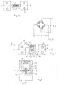
- Fig. 3 shows a preferred, simple form of an inventive elongation transmitter 1.
- Fig. 5 an example of such a strain transmitter 1 is shown attached to a structure 2 and comprising an amplifier.
- Fig. 1 shows a strain transmitter 1 according to the prior art. It has an expansion element 3 with a central axis of expansion 4, along which the expansion element 3 is stretched during a measurement.
- the expansion body 3 comprises two end regions 9, each having two fastening devices 5 and a central region 10 with a measuring element 6, which is arranged in particular also centrally between the fastening devices 5 on the axis of expansion 4.
- This measuring element 6 includes four interconnected to a full bridge 7, strain-sensitive resistors R, which are each arranged parallel or perpendicular to the axis of expansion here.
- Fig. 2 is a full bridge, as it is preferably used in the inventive arrangement, described in more detail. Each two opposite bridges between the resistors each form connections for the power supply E +, E resp.
- the strain transmitter 1 is equipped with an expansion element 3, which follows a silicon chip 8 with a full bridge integrated therein Fig. 2 includes, which outputs a voltage proportional to its elongation.
- Fig. 3 shows an inventive elongation body 3, as it is preferably installed in an inventive strain transducer 1.
- This expansion body 3 has an S-like shape, which can also resemble a mirrored S.
- This expansion element 3 in turn has two outer end regions 9, each with two fastening devices 5 and a central region 10 with the measuring element 6.
- the connections 18 of the central region to the outer regions are arranged point-symmetrically outside the elongation axis 4.
- the expansion axis 4 therefore extends twice between the fastening devices 5 outside the expansion body 3.
- the central region 10 of the expansion element 3 is rotated and warped, since it is connected only at the connections 18 with the end regions.
- the measuring element 6 detects shear stress for the inventive elongation transmitter. This is advantageous because shear stress occurs much more homogeneously than tensile stress.
- a measuring element 6 is shown with a metal sheet 11, on which, preferably in the center, the silicon chip 8 is attached over its entire surface.
- the measuring element 6 also includes a printed circuit board 13, wherein electrical contacts 12 are guided by the silicon chip 8 via the printed circuit board 13.
- the printed circuit board 13 comprises at least conductor tracks 23, which are mounted on the sheet 11 in isolation.
- the sheet 11 comprises a plug 11, which is contacted to the conductor tracks 23.
- the printed circuit board 13 may have contact points, not shown, which can be contacted directly with connections to an amplifier or to an evaluation unit.
- the silicon chip 8 When detecting shear stress, the silicon chip 8 is mounted diagonally on the sheet 11 such that the silicon chip 8 experiences the shear in the desired direction.
- the measuring element 6 is preferably mounted with its plate 11 directly on the expansion element 3 at its entire border, preferably welded. So a tight connection can be created.
- the expansion element 3 has in particular a recess 22, by means of which a connection to the printed circuit board 13 can be produced.
- Fig. 5 an elongation transmitter 1 according to the invention is shown in section, in the expansion axis 4. fastening screws 19 hold the strain transmitter 1, in particular the expansion body 3, in the end regions 9 to a structure 2 fixed.
- the expansion body 3 has a mounting plane 15, on which it bears against the structure 2. Since this expansion body 3 has an S-shape according to Fig. 3 , the Dehn Sciences 3 is not shown throughout.
- the measuring element 6 is arranged with the silicon chip 8.
- the measuring element 6 is in the mounted state only by the smallest possible distance, such as a capillary 21, almost the structure 2 at. This has the advantage the temperature of the structure is always as far as possible the same as the temperature at the measuring element 6.
- a constant current supply is applied at E +, E-.
- the detected voltage V between S + and S- reflects the measurement signal caused by the strain on the chip.
- the current local temperature T1 can also be read out.
- the bridge voltage between E + and E- is measured with constant current supply. If the static temperature on the chip 8 changes, the resistances also change without an expansion being present on the chip. This change in the bridge resistance can be detected as a change in the bridge voltage at E +, E-, whereby a first temperature T1 of the structure can be determined.
- the elongation of the structure 2 can be determined on the basis of these values V, T1 with the aid of calibration tables.
- static temperature conditions can be compensated.
- Static temperature conditions are temperatures that may be elevated or low, but are constant over time. Measurement errors due to static temperature conditions can be compensated in the manner described above.
- the chip 8 can therefore also be designed as a first temperature sensor.
- the strain transmitter 1 is also provided with an amplifier 17 with a connection 20 to a connection to an evaluation unit, not shown.
- the amplifier 17 may be plugged onto the measuring element 6 with electrical contacts or with another plug on the plug 14. In case of a malfunction of the amplifier 17, this can be easily disconnected and replaced without the strain transmitter 1 for the structure 2 must be solved.
- the amplifier 17 is a two-channel amplifier with two different output ranges. Thus it can be ensured that with the same strain transmitter both very small and very large signals can be transmitted.
- the amplifier 17 may comprise a second temperature sensor 16 for compensating for measurement errors caused by temperature fluctuations.
- a second local temperature T2 can be determined. As soon as the temperatures T1, T2 deviate from one another, static temperature conditions no longer prevail but dynamic temperature fluctuations. When determining unequal temperatures T1, T2, the determined elongation of the structure 2 can be corrected on the basis of further calibration curves by compensating the dynamic temperature fluctuations.
Landscapes
- Physics & Mathematics (AREA)
- General Physics & Mathematics (AREA)
- Measurement Of Length, Angles, Or The Like Using Electric Or Magnetic Means (AREA)
Description
- Die Erfindung betrifft einen Dehnungstransmitter zum Erfassen einer Dehnung einer Struktur, umfassend einen Dehnkörper mit einer Dehnachse mit Befestigungsvorrichtungen zum Befestigen des Dehnkörpers an einer Struktur, sowie ein Messelement, welches mittig zwischen diesen Befestigungsvorrichtungen auf der Struktur auf der Dehnachse angeordnet ist.
- Dehnungstransmitter werden beispielsweise auf Maschinenstrukturen aufgebracht, um Prozesse zu überwachen. Bei Spritzgiessmaschinen wird beispielsweise die Schliesskraft der Formwerkzeuge mit Dehnungstransmittern überwacht, wobei hierfür in der Regel DMS (Dehnmessstreifen) verwendet werden. Diese liefern sehr zuverlässige Messwerte für grosse Dehnungen, die von grossen Kräften herrühren, wie sie beim Schliessen der Werkzeuge auftreten. Andererseits sollen aber auch sehr kleine Kräfte gemessen werden können: Während der Verfahrbewegung soll eine sogenannte Formschutzfunktion das Werkzeug vor Beschädigung schützen, indem das Zufahren der Formteile sofort gestoppt wird, wenn ein Bauteil nicht korrekt entformt wurde. Dazu müssen bereits kleinste Kräfte resp. Dehnungen am Werkzeug erfasst werden können.
- Kleine Dehnungen können mit DMS weniger gut erfasst werden. Piezoelektrische Dehnungstransmitter hingegen eignen sich hervorragend zum Erfassen von kleinen wie auch von grossen Dehnungen, doch diese können leider nicht statisch messen.
- In der
GB 1456403 - Die
EP 1840500 offenbart einen Dehnungstransmitter mit einem Substrat aus monokristallinem Silizium mit zwei oder mehr Sensoren in Form von Wheatstoneschen Messbrücken aus diffundierten Widerständen. Die Sensoren sind unterschiedlich dotiert und auf dem Substrat verschieden ausgerichtet. Der an einer Struktur befestigte Dehnungstransmitter erfasst Dehnungen des Substrats richtungsspezifisch und gibt sie als Brückenquerspannungen der Wheatstoneschen Messbrücken aus. - Weiter zeigt die
US 2007017295 einen auf einer Schraube angebrachten Dehnungstransmitter mit Dehnungssensor, Wheatstoneschen Messbrücke, Analog/Digital-Wandler, Kommunikationskontroller und Antenne. Eine Dehnung in Längsrichtung der Schraube wird vom Dehnungssensor erfasst, als Brückenquerspannung der Wheatstoneschen Messbrücke ausgegeben, vom Analog/DigitalWandler digitalisiert, vom Kommunikationskontroller in ein Radiowellensignal gewandelt und von der Antenne an einen Empfänger gesendet. - Und die
US 20060207339 bezieht sich auf einen Dehnungstransmitter mit einem Dehnungssensor aus einer dünnen Metallschicht oder polykristallinem Silizium, der auf einem Substrat aus Silizium-Einkristall angeordnet ist. Der Dehnungstransmitter wird an einer Struktur befestigt und dabei so ausgerichtet, dass die Längsrichtung des Dehnungssensors parallel zur Dehnungsrichtung der zu erfassenden Dehnung der Struktur liegt. - Aufgabe der vorliegenden Erfindung ist es, einen Dehnungstransmitter eingangs beschriebener Art anzugeben, der sowohl sehr kleine wie auch sehr grosse Messwerte erfassen kann, und der auch statisch messen kann. Zudem soll er einfach zu kontaktieren sein und auch Temperaturschwankungen an der Struktur leicht kompensieren können.
- Die Aufgabe wird mit einem Dehnungstransmitter gemäß Anspruch 1 dadurch gelöst, dass das Messelement ein Blech umfasst, auf welchem ein statisch messender, zu einer Vollbrücke verschalteter, piezoresistiver Silizium Chip vollflächig angebracht ist, der eine Spannung proportional zu seiner Dehnung abgibt, wobei eine Leiterplatte am Messelement angebracht ist, die mit elektrischen Kontakten vom Silizium Chip elektrisch verbunden sind. Die Leiterplatte umfasst zum Blech isolierte Leiterbahnen, welche in einer bevorzugten Anordnung wiederum mit einem Stecker elektrisch verbunden sind, welcher ebenfalls auf dem Blech angeordnet ist. Ein solcher zu einer Vollbrücke verschalteter Silizium Chip hat eine etwa 60 mal höhere Empfindlichkeit als ein herkömmlicher, ebenfalls zu einer Vollbrücke verschalteten DMS Sensor und kann daher auch sehr tiefe Signale bis etwa einem Microstrain (1 µε), also ein 1 Mikrometer pro Meter (µm/m) erfassen. Im Gegensatz zu piezoelektrischen Sensoren gibt der zu einer Widerstandsbrücke verschaltete Silizium Chip ein Spannungssignal ab und kann statisch messen.
Da der Chip auf einem Blech angeordnet und bereits mit Kontaktierungen über eine Leiterplatte verbunden ist, kann das Messelement als solches auf seine Funktionalität überprüft werden, bevor es auf den Dehnkörper aufgebracht wird. Dadurch kann ein fehlerhafter Chip frühzeitig Identifiziert und aussortiert werden, sodass die Ausschussrate der Fertigprodukte stark reduziert werden kann.
Das Blech lässt sich auf dem Dehnkörper an seiner gesamten Umrandungen anschweissen, sodass eine dichte Verbindung entsteht.
Das Blech ist vorzugsweise auf der Unterseite des Dehnkörpers angebracht, auf welcher der Dehnkörper für die Montage an eine Montageebene der Struktur anliegt. Das Blech sollte allerdings durch einen kleinen Abstand, etwa einen Kapillarabstand von dieser Montageebene beabstandet sein, damit keine Reibung zwischen Blech und Struktur die Messung verfälscht. Die Nähe zur Struktur gewährleistet, dass die Temperatur am Messelement gleich der an der Struktur ist. Der Chip und die Leiterplatte liegen dazu auf der der Struktur abgewandter Seite des Bleches. Eine durchgehende Aussparung im Dehnkörper bis zu dessen Unterseite ermöglicht einen Zugang für einen Anschluss zum Stecker oder zu geeigneten Kontakten auf der Leiterplatte. - Die Erfindung umfasst weiter gemäß Anspruch 12 die Verwendung eines erfindungsgemäßen Dehnungstransmitters.
- Im Folgenden wird die Erfindung unter Beizug der Zeichnungen näher erklärt. Es zeigen
- Fig. 1
- eine schematische Darstellung eines Dehnungstransmitters nach dem Stand der Technik;
- Fig. 2
- Beschreibung einer Vollbrücke zur Verwendung in einem erfindungsgemässen Dehnungstransmitter;
- Fig. 3
- Darstellung eines erfindungsgemässen Dehnungstransmitters in einer bevorzugten Ausführung;
- Fig. 4
- Schematische Darstellung in der Aufsicht eines Messelementes für einen erfindungsgemässen Dehnungstransmitter;
- Fig. 5
- Schematische Darstellung im Schnitt eines erfindungsgemässen Dehnungstransmitters mit Verstärker, angebracht an einer Struktur.
- Die Erfindung betrifft einen Dehnungstransmitter 1 zum Erfassen einer Dehnung einer Struktur 2, wenn der Dehnungstransmitter 1 auf dieser angebracht ist.
Fig. 3 zeigt eine bevorzugte, einfache Form eines erfindungsgemässen Dehnungstransmitters 1. InFig. 5 ist ein Beispiel eines solchen Dehnungstransmitters 1 dargestellt, befestigt an einer Struktur 2 und umfassend einen Verstärker. -
Fig. 1 zeigt einen Dehnungstransmitter 1 nach dem Stand der Technik. Er weist einen Dehnkörper 3 auf mit einer mittleren Dehnachse 4, entlang welcher der Dehnkörper 3 während einer Messung gedehnt wird. Der Dehnkörper 3 umfasst zwei Endbereiche 9 mit jeweils zwei Befestigungsvorrichtungen 5 sowie einen mittleren Bereich 10 mit einem Messelement 6, welches insbesondere auch mittig zwischen den Befestigungsvorrichtungen 5 auf der Dehnachse 4 angeordnet ist. Dieses Messelement 6 enthält vier zu einer Vollbrücke 7 verschaltete, dehnungssensitive Widerstände R, die hier jeweils parallel oder rechtwinklig zur Dehnachse angeordnet sind. InFig. 2 wird eine Vollbrücke, wie sie bevorzugt in der erfindungsgemässen Anordnung eingesetzt wird, näher beschrieben. Je zwei gegenüberliegende Brücken zwischen den Widerständen bilden jeweils Anschlüsse für die Stromversorgung E+, E- resp. für die Spannungsabnahme S+, S- des Messsignals, das hier mit V bezeichnet wird. Im Gegensatz zu der Anordnung inFig. 1 sind die Widerstände in der Vollbrücke 7 inFig. 2 im 45° Winkel zur Dehnachse 4 angeordnet, was eine um etwa 50% erhöhte Empfindlichkeit des Messelements bewirkt gegenüber der Anordnung inFig. 1 . - Der erfindungsgemässe Dehnungstransmitter 1 ist mit einem Dehnkörper 3 ausgestattet, der einen Silizium Chip 8 mit einer darin integrierten Vollbrücke nach
Fig. 2 umfasst, der eine Spannung proportional zu seiner Dehnung abgibt. -
Fig. 3 zeigt einen erfindungsgemässen Dehnkörper 3, wie er bevorzugt in einem erfindungsgemässen Dehnungstransmitter 1 eingebaut ist. Dieser Dehnkörper 3 besitzt eine S-ähnliche Form, die auch einem gespiegelten S gleichen kann. Dieser Dehnkörper 3 weist wiederum zwei äussere Endbereiche 9 mit je zwei Befestigungsvorrichtungen 5 sowie einen mittleren Bereich 10 mit dem Messelement 6 auf. In einer erfindungsgemässen Ausführungsform sind die Verbindungen 18 des mittleren Bereichs zu den äusseren Bereichen punktsymmetrisch ausserhalb der Dehnachse 4 angeordnet. Die Dehnachse 4 verläuft daher zweimal zwischen den Befestigungsvorrichtungen 5 ausserhalb des Dehnkörpers 3. Bei einem Zug zwischen den Befestigungsvorrichtungen 5 wird der mittlere Bereich 10 des Dehnkörpers 3 gedreht und verzogen, da er nur an den Verbindungen 18 mit den Endbereichen verbunden ist. Da diese Verbindungen 18 punktsymmetrisch ausserhalb der Dehnachse 4 angeordnet sind, wirkt auf den mittleren Bereich 10 ein Moment. Vorzugsweise erfasst das Messelement 6 für den erfindungsgemässen Dehnungstransmitter Scherspannung. Dies ist von Vorteil, weil Scherspannung viel homogener auftritt als Dehnspannung. - In
Fig. 4 ist ein solches Messelement 6 mit einem Blech 11 dargestellt, auf dem, vorzugsweise mittig, der Silizium Chip 8 vollflächig angebracht ist. Das Messelement 6 umfasst zudem eine Leiterplatte 13, wobei elektrische Kontakte 12 vom Silizium Chip 8 über die Leiterplatte 13 geführt sind. Die Leiterplatte 13 umfasst zumindest Leiterbahnen 23, welche isoliert auf dem Blech 11 angebracht sind. Vorzugsweise umfasst das Blech 11 einen Stecker 11, welcher an den Leiterbahnen 23 kontaktiert ist. Andernfalls kann die Leiterplatte 13 nicht dargestellte Kontaktstellen aufweisen, welche mit Anschlüssen zu einem Verstärker oder zu einer Auswerteeinheit direkt kontaktiert werden können. - Bei der Erfassung von Scherspannung ist der Silizium Chip 8 derart diagonal auf dem Blech 11 angebracht, dass der Silizium Chip 8 die Scherung in der gewünschten Richtung erfährt.
- Das Messelement 6 ist vorzugsweise mit seinem Blech 11 direkt am Dehnkörper 3 an seiner gesamten Umrandung angebracht, vorzugsweise angeschweisst. So kann eine dichte Verbindung geschaffen werden. Innerhalb dieser Verschweissung weist der Dehnkörper 3 dazu insbesondere eine Aussparung 22 auf, durch die eine Verbindung zur Leiterplatte 13 hergestellt werden kann.
- In
Fig. 5 ist ein erfindungsgemässer Dehnungstransmitter 1 im Schnitt dargestellt, in der Dehnachse 4. Befestigungsschrauben 19 halten den Dehnungstransmitter 1, insbesondere den Dehnkörper 3, in den Endbereichen 9 an einer Struktur 2 fest. Der Dehnkörper 3 weist eine Montageebene 15 auf, an welcher er an der Struktur 2 anliegt. Da dieser Dehnkörper 3 eine S-Form aufweist gemässFig. 3 , ist der Dehnkörper 3 nicht durchgehend dargestellt. Im mittleren Bereich 10 ist das Messelement 6 mit dem Silizium Chip 8 angeordnet. - Erfindungsgemäss liegt das Messelement 6 im montierten Zustand nur durch einen möglichst kleinen Abstand, etwa einen Kapillarabstand 21, fast der Struktur 2 an. Dies hat den Vorteil, dass die Temperatur der Struktur stets möglichst dieselbe ist wie die Temperatur am Messelement 6.
- Für eine Messung am Silicium Chip 8 wird jeweils eine konstante Stromspeisung bei E+, E- angelegt. Die erfasste Spannung V zwischen S+ und S- gibt das Messsignal wieder, das durch die Dehnung am Chip verursacht wird. Am Silizium Chip 8 kann erfindungsgemäss zusätzlich zum dehnungsbedingten Spannungswert V auch die aktuelle lokale Temperatur T1 ausgelesen werden. Dazu wird die Brückenspannung zwischen E+ und E- bei konstanter Stromspeisung gemessen. Ändert sich die statische Temperatur am Chip 8, so verändern sich auch die Widerstände, ohne dass eine Dehnung am Chip vorliegt. Diese Änderung des Brückenwiderstandes kann als Änderung der Brückenspannung bei E+, E- erfasst werden, wodurch eine erste Temperatur T1 der Struktur ermittelt werden kann.
- Die Dehnung der Struktur 2 kann auf Grund dieser Werte V, T1 unter Mithilfe von Eichtabellen ermittelt werden. So können statische Temperaturverhältnisse kompensiert werden. Statische Temperaturverhältnisse sind Temperaturen, welche erhöht oder tief sein können, jedoch über längere Zeit konstant sind. Messfehler, bedingt durch statische Temperaturverhältnisse, können auf die oben beschriebene Art kompensiert werden. Der Chip 8 kann demnach auch als erster Temperaturfühler ausgestaltet sein.
- Vorzugsweise ist der Dehnungstransmitter 1 auch mit einem Verstärker 17 mit einem Anschluss 20 zu einer Verbindung zu einer nicht dargestellten Auswerteeinheit versehen. Insbesondere kann der Verstärker 17 auf dem Messelement 6 mit elektrischen Kontakten oder mit einem weiteren Stecker auf dem Stecker 14 aufgesteckt sein. Bei einer Fehlfunktion des Verstärkers 17 kann dieser einfach abgesteckt und ersetzt werden, ohne dass der Dehnungstransmitter 1 dafür von der Struktur 2 gelöst werden muss.
- Vorzugsweise ist der Verstärker 17 ein Zweikanalverstärker mit zwei unterschiedlichen Ausgabebereichen. So kann gewährleistet werden, dass mit demselben Dehnungstransmitter sowohl sehr kleine wie auch sehr grosse Signale übermittelt werden können.
- Der Verstärker 17 kann insbesondere einen zweiten Temperaturfühler 16 umfassen zum Kompensieren von Messfehlern, die von Temperaturschwankungen verursacht werden.
- Unter Verwendung eines zusätzlichen Temperaturfühlers 16 kann eine zweite lokale Temperatur T2 ermittelt werden. Sobald die Temperaturen T1, T2 voneinander abweichen, herrschen keine statischen Temperaturverhältnisse mehr, sondern dynamische Temperaturschwankungen. Bei der Feststellung von ungleichen Temperaturen T1, T2 kann auf Grund von weiteren Eichkurven die ermittelte Dehnung der Struktur 2 korrigiert werden, indem die dynamischen Temperaturschwankungen kompensiert werden.
-
- 1
- Dehnungstransmitter
- 2
- Struktur
- 3
- Dehnkörper
- 4
- Dehnachse
- 5
- Befestigungsvorrichtungen
- 6
- Messelement
- 7
- Vollbrücke
- 8
- Silizium Chip
- 9
- Endbereich
- 10
- Mittlerer Bereich
- 11
- Blech
- 12
- Elektrische Kontakte
- 13
- Leiterplatte
- 14
- Stecker
- 15
- Montageebene
- 16
- zweiter Temperaturfühler
- 17
- Verstärker
- 18
- Verbindungen
- 19
- Befestigungsschrauben
- 20
- Anschluss
- 21
- Kapillarabstand
- 22
- Aussparung
- 23
- Isolierte Leiterbahnen
- R
- Widerstand
- E+, E-
- Stromversorgung
- S+, S-
- Spannungsabnehme des Messsignals
- V
- Spannung zur Ermittlung der Dehnung
- T1
- Temperatur am Blech und an der Struktur
- T2
- Temperatur entfernt von der Struktur, Umgebungstemperatur
Claims (13)
- Dehnungstransmitter (1) zum Erfassen einer Dehnung einer Struktur (2), umfassend einen Dehnkörper (3) mit einer Dehnachse (4) entlang welcher der Dehnkörper (3) während einer Messung dehnbar ist und mit Befestigungsvorrichtungen (5) zum Befestigen des Dehnkörpers (3) an einer Struktur (2), sowie ein Messelement (6), welches mittig zwischen diesen Befestigungsvorrichtungen (5) auf der Struktur (2) auf der Dehnachse (4) angeordnet ist, dadurch gekennzeichnet, dass das Messelement (6) ein Blech (11) umfasst, auf welchem ein statisch messender, zu einer Vollbrücke (7) verschalteter piezoresistiver Silizium Chip (8) vollflächig angebracht ist; dass das Blech (11) auf dem Dehnkörper (3) angebracht ist; dass der piezoresistive Silizium Chip (8) im gedehnten Zustand eine Spannung proportional zu seiner Dehnung abgibt; und dass das Messelement (6) eine Leiterplatte (13) umfasst, wobei elektrische Kontakte (12) vom Silizium Chip (8) über die Leiterplatte (13) als isoliert auf dem Blech (11) angebrachte Leiterbahnen (23) geführt sind.
- Dehnungstransmitter (1) nach Anspruch 1, dadurch gekennzeichnet, dass das Messelement einen Stecker (14) umfasst, wobei elektrische Kontakte (12) vom Silizium Chip (8) über die Leiterplatte (13) als isoliert auf dem Blech (11) angebrachte Leiterbahnen (23) zum Stecker (14) geführt sind.
- Dehnungstransmitter (1) nach einem der vorhergehenden Ansprüche, dadurch gekennzeichnet, dass die Vollbrücke (7) Widerstände umfasst, welche im 45° Winkel zur Dehnachse (4) angeordnet sind.
- Dehnungstransmitter (1) nach einem der vorhergehenden Ansprüche, dadurch gekennzeichnet, dass der Dehnkörper (2) eine S-ähnliche Form aufweist mit zwei äusseren Endbereichen (9) mit den Befestigungsvorrichtungen (5) sowie mit einem mittleren Bereich (10) mit dem Messelement (6), wobei die Verbindungen des mittleren Bereichs zu den äusseren Bereichen punktsymmetrisch ausserhalb der Dehnachse (4) angeordnet sind.
- Dehnungstransmitter (1) nach einem der vorhergehenden Ansprüche, dadurch gekennzeichnet, dass das Messelement (6) bei einer Dehnung des Dehnkörpers (3) eine Scherspannung erfassen kann.
- Dehnungstransmitter (1) nach einem der vorhergehenden Ansprüche, umfassend eine Montageebene (15) des Dehnkörpers (3), an welcher der Dehnkörper (3) im montierten Zustand an der Struktur (2) anliegt, dadurch gekennzeichnet, dass das Messelement (6) mit einem Kapillarabstand (21) an der Struktur (2) anliegt.
- Dehnungstransmitter (1) nach einem der vorhergehenden Ansprüche, dadurch gekennzeichnet, dass der Silizium Chip (8) einen ersten Temperaturfühler umfasst zum Kompensieren von Messfehlern, die von Temperaturschwankungen verursacht werden.
- Dehnungstransmitter (1) nacheinem der vorhergehenden Ansprüche, dadurch gekennzeichnet, dass er einen Verstärker (17) umfasst mit einem Anschluss (20) zu einer Verbindung zu einer Auswerteeinheit.
- Dehnungstransmitter (1) nach Anspruch 8, dadurch gekennzeichnet, dass der Verstärker (17) auf dem Messelement (6) mit elektrischen Kontakten (12) aufgesteckt ist, vorzugsweise auf einem Stecker (14), der auf dem Blech (8) angebracht ist.
- Dehnungstransmitter (1) nach einem der Ansprüche 8 oder 9, dadurch gekennzeichnet, dass der Verstärker (17) ein Zweikanalverstärker ist mit zwei unterschiedlichen Ausgabebereichen.
- Dehnungstransmitter (1) nach Anspruch 7 und einem der Ansprüche 8 bis 10, dadurch gekennzeichnet, dass der Verstärker (17) einen zweiten Temperaturfühler (16) umfasst zum Kompensieren von Messfehlern, die von dynamischen Temperaturschwankungen verursacht werden.
- Verfahren zum Erfassen einer Dehnung einer Struktur (2) unter Verwendung eines Dehnungstransmitters (1) nach Anspruch 7 mit einem ersten Temperaturfühler, dadurch gekennzeichnet, dass am Silizium Chip (8) der dehnungsbedingte Spannungswert V sowie die aktuelle lokale Temperatur T1 ausgelesen wird und dass die Dehnung der Struktur (2) auf Grund dieser Werte V, T1 sowie auf Grund von Eichtabellen ermittelt wird zum Kompensieren von statischen Temperaturverhältnissen.
- Verfahren nach Anspruch 12 unter Verwendung eines Dehnungstransmitters (1) nach Anspruch 11 mit einem zweiten Temperaturfühler (16), dadurch gekennzeichnet, dass am zweiten Temperaturfühler (16) eine zweite lokale Temperatur T2 ermittelt wird, wobei bei Feststellung von ungleichen Temperaturen T1, T2 die ermittelte Dehnung der Struktur (2) korrigiert wird zum Kompensieren von dynamischen Temperaturschwankungen.
Applications Claiming Priority (2)
| Application Number | Priority Date | Filing Date | Title |
|---|---|---|---|
| CH01742/12A CH707008A1 (de) | 2012-09-27 | 2012-09-27 | Dehnungstransmitter. |
| PCT/CH2013/000172 WO2014047743A1 (de) | 2012-09-27 | 2013-09-27 | Dehnungstransmitter |
Publications (2)
| Publication Number | Publication Date |
|---|---|
| EP2901100A1 EP2901100A1 (de) | 2015-08-05 |
| EP2901100B1 true EP2901100B1 (de) | 2018-11-07 |
Family
ID=46940174
Family Applications (1)
| Application Number | Title | Priority Date | Filing Date |
|---|---|---|---|
| EP13773168.3A Not-in-force EP2901100B1 (de) | 2012-09-27 | 2013-09-27 | Dehnungstransmitter |
Country Status (7)
| Country | Link |
|---|---|
| US (1) | US9689757B2 (de) |
| EP (1) | EP2901100B1 (de) |
| JP (1) | JP6203850B2 (de) |
| KR (1) | KR101808928B1 (de) |
| CN (1) | CN104685314B (de) |
| CH (1) | CH707008A1 (de) |
| WO (1) | WO2014047743A1 (de) |
Families Citing this family (8)
| Publication number | Priority date | Publication date | Assignee | Title |
|---|---|---|---|---|
| US9726587B2 (en) * | 2015-01-30 | 2017-08-08 | Stmicroelectronics S.R.L. | Tensile stress measurement device with attachment plates and related methods |
| CN106885509A (zh) * | 2017-04-10 | 2017-06-23 | 广西交通科学研究院有限公司 | 考虑温度影响的应变测试装置 |
| CN106969701B (zh) * | 2017-04-10 | 2019-04-19 | 广西交通科学研究院有限公司 | 应变测试中温度影响的修正方法 |
| JP6633581B2 (ja) | 2017-08-28 | 2020-01-22 | ファナック株式会社 | 検出装置 |
| CN108303201A (zh) * | 2017-12-28 | 2018-07-20 | 上海交通大学 | 面向智能加工的多通道高带宽无线力传感器 |
| WO2020260205A1 (en) | 2019-06-24 | 2020-12-30 | Albert-Ludwigs-Universität Freiburg | Tactile sensor and method for operating a tactile sensor |
| CN110608826B (zh) * | 2019-10-09 | 2024-09-10 | 安徽华电工程咨询设计有限公司 | 一种动态测量电机实时应力的装置 |
| CN111426413A (zh) * | 2020-05-15 | 2020-07-17 | 罕王微电子(辽宁)有限公司 | 一种新型压力传感器及设计方法 |
Family Cites Families (16)
| Publication number | Priority date | Publication date | Assignee | Title |
|---|---|---|---|---|
| GB1456403A (en) * | 1974-01-04 | 1976-11-24 | Welwyn Electric Ltd | Transducers |
| GB1469644A (en) * | 1975-01-17 | 1977-04-06 | Welwyn Electric Ltd | Transducers |
| DE2841312C2 (de) * | 1978-09-22 | 1985-06-05 | Robert Bosch Gmbh, 7000 Stuttgart | Monolithischer Halbleiter-Drucksensor und Verfahren zu dessen Herstellung |
| JPS58118920A (ja) | 1982-01-11 | 1983-07-15 | Kubota Ltd | 計数器 |
| JPH0765922B2 (ja) | 1987-02-02 | 1995-07-19 | 株式会社島津製作所 | 電子天びん |
| JPH0475931U (de) | 1990-11-14 | 1992-07-02 | ||
| JPH0666621U (ja) | 1993-01-13 | 1994-09-20 | 株式会社東海理化電機製作所 | 圧力センサ |
| US20020166385A1 (en) | 2001-05-08 | 2002-11-14 | Terry Bloom | Strain sensor incorporating a steel substrate |
| JP4617943B2 (ja) | 2005-03-18 | 2011-01-26 | 株式会社日立製作所 | 力学量測定装置 |
| US7293466B2 (en) | 2005-07-19 | 2007-11-13 | Hitachi, Ltd. | Bolt with function of measuring strain |
| JP4697004B2 (ja) | 2006-03-29 | 2011-06-08 | 株式会社日立製作所 | 力学量測定装置 |
| EP2035771B1 (de) | 2006-05-30 | 2009-10-21 | The Timken Company | Sensor für verschiebung, dehnung und kraft |
| US7441467B2 (en) * | 2006-07-12 | 2008-10-28 | Cts Corporation | Compression strain sensor |
| JP2009128153A (ja) | 2007-11-22 | 2009-06-11 | Aisin Seiki Co Ltd | 車両用のシート用荷重検知センサ |
| CN101608960B (zh) | 2009-07-27 | 2011-02-16 | 广州粤能电力科技开发有限公司 | 一种确定传感器应变片的粘贴位置的方法 |
| GB201007813D0 (en) * | 2010-05-11 | 2010-06-23 | Sondex Wireline Ltd | A load cell for a downhole load measuring tool |
-
2012
- 2012-09-27 CH CH01742/12A patent/CH707008A1/de not_active Application Discontinuation
-
2013
- 2013-09-27 KR KR1020157007503A patent/KR101808928B1/ko not_active Expired - Fee Related
- 2013-09-27 WO PCT/CH2013/000172 patent/WO2014047743A1/de not_active Ceased
- 2013-09-27 US US14/428,522 patent/US9689757B2/en not_active Expired - Fee Related
- 2013-09-27 EP EP13773168.3A patent/EP2901100B1/de not_active Not-in-force
- 2013-09-27 JP JP2015533388A patent/JP6203850B2/ja not_active Expired - Fee Related
- 2013-09-27 CN CN201380050583.2A patent/CN104685314B/zh not_active Expired - Fee Related
Non-Patent Citations (1)
| Title |
|---|
| None * |
Also Published As
| Publication number | Publication date |
|---|---|
| CN104685314A (zh) | 2015-06-03 |
| KR20150058249A (ko) | 2015-05-28 |
| EP2901100A1 (de) | 2015-08-05 |
| JP6203850B2 (ja) | 2017-09-27 |
| JP2015530579A (ja) | 2015-10-15 |
| CH707008A1 (de) | 2014-03-31 |
| KR101808928B1 (ko) | 2017-12-13 |
| US20150233777A1 (en) | 2015-08-20 |
| CN104685314B (zh) | 2017-09-19 |
| WO2014047743A1 (de) | 2014-04-03 |
| US9689757B2 (en) | 2017-06-27 |
Similar Documents
| Publication | Publication Date | Title |
|---|---|---|
| EP2901100A1 (de) | Dehnungstransmitter | |
| EP1460398B1 (de) | Dehnungsmessfühler mit resistiven und piezoelektrischen dehnungsempfindlichen Elementen | |
| EP0776466B1 (de) | Kraft- oder dehnungssensor | |
| DE3429250C1 (de) | Auf die Einwirkung einer Kraft ansprechender Sensor | |
| EP2715300B1 (de) | Sensor für die messung von druck und/oder kraft | |
| DE102018122522A1 (de) | Drucksensor mit verbessertem Dehnungsmessstreifen | |
| DE102019218334A1 (de) | Mikromechanische Vorrichtung mit lokaler Temperaturerfassung | |
| EP0215140A1 (de) | Drucksensor | |
| DE102011002884A1 (de) | Elektronische Kraft- und/oder Druck- und/oder Temperaturmessschaltung | |
| WO2004057291A1 (de) | Differenzdrucksensor | |
| DE102004033925B4 (de) | Drehmoment-Messaufnehmer | |
| EP2585802A1 (de) | Piezoresistiver kraftsensor | |
| WO2004005858A1 (de) | Messeinrichtung mit plausibilitätskontrolle | |
| DE19752439C2 (de) | Mikromechanischer Neigungssensor, insbesondere für Kraftfahrzeuge | |
| DE202016008592U1 (de) | Sensor | |
| DE102008041771B4 (de) | Messvorrichtung mit verstimmbarem Widerstand | |
| DE19806753A1 (de) | Sensormodul | |
| WO2016016026A1 (de) | Drucksensor und verfahren zum herstellen eines drucksensors | |
| DE102024129151B3 (de) | Verfahren zur Funktionsüberwachung eines Druckmessgeräts | |
| WO2015154771A1 (de) | Messelement und ein messelement aufweisendes bauteil | |
| DE102011006922B4 (de) | Messwandler für die Sensortechnik | |
| DE102011105539B4 (de) | Vorrichtung zum Wandeln einer Kraft in ein elektrisches Signal, insbesondere piezoresistiver Kraftsensor | |
| DE102008055774B4 (de) | Vorrichtung zum Messen einer Temperatur eines Bauteils und Vorrichtung zum Messen einer Dehnung eines Bauteils | |
| DE102007054027B4 (de) | Vorrichtung und Verfahren zur kapazitiven Kraftmessung | |
| DE102021118886B3 (de) | Druckmittler mit Test-Klebeschicht und Verfahren zum Überwachen eines Druckmittlers |
Legal Events
| Date | Code | Title | Description |
|---|---|---|---|
| PUAI | Public reference made under article 153(3) epc to a published international application that has entered the european phase |
Free format text: ORIGINAL CODE: 0009012 |
|
| 17P | Request for examination filed |
Effective date: 20150415 |
|
| AK | Designated contracting states |
Kind code of ref document: A1 Designated state(s): AL AT BE BG CH CY CZ DE DK EE ES FI FR GB GR HR HU IE IS IT LI LT LU LV MC MK MT NL NO PL PT RO RS SE SI SK SM TR |
|
| AX | Request for extension of the european patent |
Extension state: BA ME |
|
| DAX | Request for extension of the european patent (deleted) | ||
| GRAP | Despatch of communication of intention to grant a patent |
Free format text: ORIGINAL CODE: EPIDOSNIGR1 |
|
| STAA | Information on the status of an ep patent application or granted ep patent |
Free format text: STATUS: GRANT OF PATENT IS INTENDED |
|
| INTG | Intention to grant announced |
Effective date: 20180518 |
|
| GRAJ | Information related to disapproval of communication of intention to grant by the applicant or resumption of examination proceedings by the epo deleted |
Free format text: ORIGINAL CODE: EPIDOSDIGR1 |
|
| STAA | Information on the status of an ep patent application or granted ep patent |
Free format text: STATUS: REQUEST FOR EXAMINATION WAS MADE |
|
| GRAS | Grant fee paid |
Free format text: ORIGINAL CODE: EPIDOSNIGR3 |
|
| STAA | Information on the status of an ep patent application or granted ep patent |
Free format text: STATUS: GRANT OF PATENT IS INTENDED |
|
| INTC | Intention to grant announced (deleted) | ||
| GRAP | Despatch of communication of intention to grant a patent |
Free format text: ORIGINAL CODE: EPIDOSNIGR1 |
|
| INTG | Intention to grant announced |
Effective date: 20180907 |
|
| GRAA | (expected) grant |
Free format text: ORIGINAL CODE: 0009210 |
|
| STAA | Information on the status of an ep patent application or granted ep patent |
Free format text: STATUS: THE PATENT HAS BEEN GRANTED |
|
| AK | Designated contracting states |
Kind code of ref document: B1 Designated state(s): AL AT BE BG CH CY CZ DE DK EE ES FI FR GB GR HR HU IE IS IT LI LT LU LV MC MK MT NL NO PL PT RO RS SE SI SK SM TR |
|
| REG | Reference to a national code |
Ref country code: GB Ref legal event code: FG4D Free format text: NOT ENGLISH |
|
| REG | Reference to a national code |
Ref country code: CH Ref legal event code: EP Ref country code: AT Ref legal event code: REF Ref document number: 1062576 Country of ref document: AT Kind code of ref document: T Effective date: 20181115 |
|
| REG | Reference to a national code |
Ref country code: DE Ref legal event code: R096 Ref document number: 502013011558 Country of ref document: DE |
|
| REG | Reference to a national code |
Ref country code: IE Ref legal event code: FG4D Free format text: LANGUAGE OF EP DOCUMENT: GERMAN |
|
| REG | Reference to a national code |
Ref country code: NL Ref legal event code: MP Effective date: 20181107 |
|
| REG | Reference to a national code |
Ref country code: LT Ref legal event code: MG4D |
|
| PG25 | Lapsed in a contracting state [announced via postgrant information from national office to epo] |
Ref country code: LV Free format text: LAPSE BECAUSE OF FAILURE TO SUBMIT A TRANSLATION OF THE DESCRIPTION OR TO PAY THE FEE WITHIN THE PRESCRIBED TIME-LIMIT Effective date: 20181107 Ref country code: ES Free format text: LAPSE BECAUSE OF FAILURE TO SUBMIT A TRANSLATION OF THE DESCRIPTION OR TO PAY THE FEE WITHIN THE PRESCRIBED TIME-LIMIT Effective date: 20181107 Ref country code: BG Free format text: LAPSE BECAUSE OF FAILURE TO SUBMIT A TRANSLATION OF THE DESCRIPTION OR TO PAY THE FEE WITHIN THE PRESCRIBED TIME-LIMIT Effective date: 20190207 Ref country code: NO Free format text: LAPSE BECAUSE OF FAILURE TO SUBMIT A TRANSLATION OF THE DESCRIPTION OR TO PAY THE FEE WITHIN THE PRESCRIBED TIME-LIMIT Effective date: 20190207 Ref country code: HR Free format text: LAPSE BECAUSE OF FAILURE TO SUBMIT A TRANSLATION OF THE DESCRIPTION OR TO PAY THE FEE WITHIN THE PRESCRIBED TIME-LIMIT Effective date: 20181107 Ref country code: LT Free format text: LAPSE BECAUSE OF FAILURE TO SUBMIT A TRANSLATION OF THE DESCRIPTION OR TO PAY THE FEE WITHIN THE PRESCRIBED TIME-LIMIT Effective date: 20181107 Ref country code: IS Free format text: LAPSE BECAUSE OF FAILURE TO SUBMIT A TRANSLATION OF THE DESCRIPTION OR TO PAY THE FEE WITHIN THE PRESCRIBED TIME-LIMIT Effective date: 20190307 Ref country code: FI Free format text: LAPSE BECAUSE OF FAILURE TO SUBMIT A TRANSLATION OF THE DESCRIPTION OR TO PAY THE FEE WITHIN THE PRESCRIBED TIME-LIMIT Effective date: 20181107 |
|
| PG25 | Lapsed in a contracting state [announced via postgrant information from national office to epo] |
Ref country code: NL Free format text: LAPSE BECAUSE OF FAILURE TO SUBMIT A TRANSLATION OF THE DESCRIPTION OR TO PAY THE FEE WITHIN THE PRESCRIBED TIME-LIMIT Effective date: 20181107 Ref country code: AL Free format text: LAPSE BECAUSE OF FAILURE TO SUBMIT A TRANSLATION OF THE DESCRIPTION OR TO PAY THE FEE WITHIN THE PRESCRIBED TIME-LIMIT Effective date: 20181107 Ref country code: SE Free format text: LAPSE BECAUSE OF FAILURE TO SUBMIT A TRANSLATION OF THE DESCRIPTION OR TO PAY THE FEE WITHIN THE PRESCRIBED TIME-LIMIT Effective date: 20181107 Ref country code: GR Free format text: LAPSE BECAUSE OF FAILURE TO SUBMIT A TRANSLATION OF THE DESCRIPTION OR TO PAY THE FEE WITHIN THE PRESCRIBED TIME-LIMIT Effective date: 20190208 Ref country code: RS Free format text: LAPSE BECAUSE OF FAILURE TO SUBMIT A TRANSLATION OF THE DESCRIPTION OR TO PAY THE FEE WITHIN THE PRESCRIBED TIME-LIMIT Effective date: 20181107 Ref country code: PT Free format text: LAPSE BECAUSE OF FAILURE TO SUBMIT A TRANSLATION OF THE DESCRIPTION OR TO PAY THE FEE WITHIN THE PRESCRIBED TIME-LIMIT Effective date: 20190307 |
|
| PG25 | Lapsed in a contracting state [announced via postgrant information from national office to epo] |
Ref country code: DK Free format text: LAPSE BECAUSE OF FAILURE TO SUBMIT A TRANSLATION OF THE DESCRIPTION OR TO PAY THE FEE WITHIN THE PRESCRIBED TIME-LIMIT Effective date: 20181107 Ref country code: PL Free format text: LAPSE BECAUSE OF FAILURE TO SUBMIT A TRANSLATION OF THE DESCRIPTION OR TO PAY THE FEE WITHIN THE PRESCRIBED TIME-LIMIT Effective date: 20181107 |
|
| REG | Reference to a national code |
Ref country code: DE Ref legal event code: R097 Ref document number: 502013011558 Country of ref document: DE |
|
| PG25 | Lapsed in a contracting state [announced via postgrant information from national office to epo] |
Ref country code: SK Free format text: LAPSE BECAUSE OF FAILURE TO SUBMIT A TRANSLATION OF THE DESCRIPTION OR TO PAY THE FEE WITHIN THE PRESCRIBED TIME-LIMIT Effective date: 20181107 Ref country code: RO Free format text: LAPSE BECAUSE OF FAILURE TO SUBMIT A TRANSLATION OF THE DESCRIPTION OR TO PAY THE FEE WITHIN THE PRESCRIBED TIME-LIMIT Effective date: 20181107 Ref country code: EE Free format text: LAPSE BECAUSE OF FAILURE TO SUBMIT A TRANSLATION OF THE DESCRIPTION OR TO PAY THE FEE WITHIN THE PRESCRIBED TIME-LIMIT Effective date: 20181107 Ref country code: SM Free format text: LAPSE BECAUSE OF FAILURE TO SUBMIT A TRANSLATION OF THE DESCRIPTION OR TO PAY THE FEE WITHIN THE PRESCRIBED TIME-LIMIT Effective date: 20181107 |
|
| PLBE | No opposition filed within time limit |
Free format text: ORIGINAL CODE: 0009261 |
|
| STAA | Information on the status of an ep patent application or granted ep patent |
Free format text: STATUS: NO OPPOSITION FILED WITHIN TIME LIMIT |
|
| 26N | No opposition filed |
Effective date: 20190808 |
|
| PG25 | Lapsed in a contracting state [announced via postgrant information from national office to epo] |
Ref country code: SI Free format text: LAPSE BECAUSE OF FAILURE TO SUBMIT A TRANSLATION OF THE DESCRIPTION OR TO PAY THE FEE WITHIN THE PRESCRIBED TIME-LIMIT Effective date: 20181107 |
|
| PGFP | Annual fee paid to national office [announced via postgrant information from national office to epo] |
Ref country code: CZ Payment date: 20190827 Year of fee payment: 7 Ref country code: IT Payment date: 20190925 Year of fee payment: 7 Ref country code: FR Payment date: 20190927 Year of fee payment: 7 Ref country code: DE Payment date: 20190918 Year of fee payment: 7 |
|
| PGFP | Annual fee paid to national office [announced via postgrant information from national office to epo] |
Ref country code: AT Payment date: 20190919 Year of fee payment: 7 Ref country code: GB Payment date: 20190920 Year of fee payment: 7 |
|
| PG25 | Lapsed in a contracting state [announced via postgrant information from national office to epo] |
Ref country code: TR Free format text: LAPSE BECAUSE OF FAILURE TO SUBMIT A TRANSLATION OF THE DESCRIPTION OR TO PAY THE FEE WITHIN THE PRESCRIBED TIME-LIMIT Effective date: 20181107 |
|
| PGFP | Annual fee paid to national office [announced via postgrant information from national office to epo] |
Ref country code: CH Payment date: 20191203 Year of fee payment: 7 |
|
| PG25 | Lapsed in a contracting state [announced via postgrant information from national office to epo] |
Ref country code: MC Free format text: LAPSE BECAUSE OF FAILURE TO SUBMIT A TRANSLATION OF THE DESCRIPTION OR TO PAY THE FEE WITHIN THE PRESCRIBED TIME-LIMIT Effective date: 20181107 |
|
| PG25 | Lapsed in a contracting state [announced via postgrant information from national office to epo] |
Ref country code: LU Free format text: LAPSE BECAUSE OF NON-PAYMENT OF DUE FEES Effective date: 20190927 Ref country code: IE Free format text: LAPSE BECAUSE OF NON-PAYMENT OF DUE FEES Effective date: 20190927 |
|
| REG | Reference to a national code |
Ref country code: BE Ref legal event code: MM Effective date: 20190930 |
|
| PG25 | Lapsed in a contracting state [announced via postgrant information from national office to epo] |
Ref country code: BE Free format text: LAPSE BECAUSE OF NON-PAYMENT OF DUE FEES Effective date: 20190930 |
|
| REG | Reference to a national code |
Ref country code: DE Ref legal event code: R119 Ref document number: 502013011558 Country of ref document: DE |
|
| PG25 | Lapsed in a contracting state [announced via postgrant information from national office to epo] |
Ref country code: CZ Free format text: LAPSE BECAUSE OF NON-PAYMENT OF DUE FEES Effective date: 20200927 |
|
| REG | Reference to a national code |
Ref country code: CH Ref legal event code: PL |
|
| REG | Reference to a national code |
Ref country code: AT Ref legal event code: MM01 Ref document number: 1062576 Country of ref document: AT Kind code of ref document: T Effective date: 20200927 |
|
| GBPC | Gb: european patent ceased through non-payment of renewal fee |
Effective date: 20200927 |
|
| PG25 | Lapsed in a contracting state [announced via postgrant information from national office to epo] |
Ref country code: CY Free format text: LAPSE BECAUSE OF FAILURE TO SUBMIT A TRANSLATION OF THE DESCRIPTION OR TO PAY THE FEE WITHIN THE PRESCRIBED TIME-LIMIT Effective date: 20181107 |
|
| PG25 | Lapsed in a contracting state [announced via postgrant information from national office to epo] |
Ref country code: HU Free format text: LAPSE BECAUSE OF FAILURE TO SUBMIT A TRANSLATION OF THE DESCRIPTION OR TO PAY THE FEE WITHIN THE PRESCRIBED TIME-LIMIT; INVALID AB INITIO Effective date: 20130927 Ref country code: MT Free format text: LAPSE BECAUSE OF FAILURE TO SUBMIT A TRANSLATION OF THE DESCRIPTION OR TO PAY THE FEE WITHIN THE PRESCRIBED TIME-LIMIT Effective date: 20181107 Ref country code: DE Free format text: LAPSE BECAUSE OF NON-PAYMENT OF DUE FEES Effective date: 20210401 Ref country code: FR Free format text: LAPSE BECAUSE OF NON-PAYMENT OF DUE FEES Effective date: 20200930 |
|
| PG25 | Lapsed in a contracting state [announced via postgrant information from national office to epo] |
Ref country code: LI Free format text: LAPSE BECAUSE OF NON-PAYMENT OF DUE FEES Effective date: 20200930 Ref country code: GB Free format text: LAPSE BECAUSE OF NON-PAYMENT OF DUE FEES Effective date: 20200927 Ref country code: CH Free format text: LAPSE BECAUSE OF NON-PAYMENT OF DUE FEES Effective date: 20200930 Ref country code: AT Free format text: LAPSE BECAUSE OF NON-PAYMENT OF DUE FEES Effective date: 20200927 |
|
| PG25 | Lapsed in a contracting state [announced via postgrant information from national office to epo] |
Ref country code: IT Free format text: LAPSE BECAUSE OF NON-PAYMENT OF DUE FEES Effective date: 20200927 |
|
| PG25 | Lapsed in a contracting state [announced via postgrant information from national office to epo] |
Ref country code: MK Free format text: LAPSE BECAUSE OF FAILURE TO SUBMIT A TRANSLATION OF THE DESCRIPTION OR TO PAY THE FEE WITHIN THE PRESCRIBED TIME-LIMIT Effective date: 20181107 |