EP2901504B1 - Composant électrique et procédé d'établissement d'une mise en contact électrique d'un composant électrique - Google Patents
Composant électrique et procédé d'établissement d'une mise en contact électrique d'un composant électrique Download PDFInfo
- Publication number
- EP2901504B1 EP2901504B1 EP13762093.6A EP13762093A EP2901504B1 EP 2901504 B1 EP2901504 B1 EP 2901504B1 EP 13762093 A EP13762093 A EP 13762093A EP 2901504 B1 EP2901504 B1 EP 2901504B1
- Authority
- EP
- European Patent Office
- Prior art keywords
- metallization
- electrical component
- contact
- contact element
- component according
- Prior art date
- Legal status (The legal status is an assumption and is not a legal conclusion. Google has not performed a legal analysis and makes no representation as to the accuracy of the status listed.)
- Active
Links
Images

Classifications
-
- H—ELECTRICITY
- H01—ELECTRIC ELEMENTS
- H01H—ELECTRIC SWITCHES; RELAYS; SELECTORS; EMERGENCY PROTECTIVE DEVICES
- H01H57/00—Electrostrictive relays; Piezoelectric relays
-
- H—ELECTRICITY
- H01—ELECTRIC ELEMENTS
- H01H—ELECTRIC SWITCHES; RELAYS; SELECTORS; EMERGENCY PROTECTIVE DEVICES
- H01H45/00—Details of relays
- H01H45/14—Terminal arrangements
-
- H—ELECTRICITY
- H01—ELECTRIC ELEMENTS
- H01H—ELECTRIC SWITCHES; RELAYS; SELECTORS; EMERGENCY PROTECTIVE DEVICES
- H01H49/00—Apparatus or processes specially adapted to the manufacture of relays or parts thereof
-
- H—ELECTRICITY
- H10—SEMICONDUCTOR DEVICES; ELECTRIC SOLID-STATE DEVICES NOT OTHERWISE PROVIDED FOR
- H10N—ELECTRIC SOLID-STATE DEVICES NOT OTHERWISE PROVIDED FOR
- H10N30/00—Piezoelectric or electrostrictive devices
- H10N30/01—Manufacture or treatment
- H10N30/06—Forming electrodes or interconnections, e.g. leads or terminals
- H10N30/063—Forming interconnections, e.g. connection electrodes of multilayered piezoelectric or electrostrictive parts
-
- H—ELECTRICITY
- H10—SEMICONDUCTOR DEVICES; ELECTRIC SOLID-STATE DEVICES NOT OTHERWISE PROVIDED FOR
- H10N—ELECTRIC SOLID-STATE DEVICES NOT OTHERWISE PROVIDED FOR
- H10N30/00—Piezoelectric or electrostrictive devices
- H10N30/80—Constructional details
- H10N30/87—Electrodes or interconnections, e.g. leads or terminals
- H10N30/872—Interconnections, e.g. connection electrodes of multilayer piezoelectric or electrostrictive devices
Definitions
- An electrical component comprising at least one metallization is specified.
- the metallization is provided for contacting internal electrodes of the component.
- the electrical component is formed for example as a piezoelectric actuator.
- a method for producing a contact of an electrical component is specified.
- a piezoactuator which has an external contact, in which a wire mesh is attached to a base metallization.
- EP 0844678 B1 is a piezoelectric actuator specified, which has a three-dimensionally structured, electrically conductive electrode which is connected via partial contact points with a base metallization.
- EP 2 437 322 A1 For example, a piezoelectric device with a two-layered baked external electrode is known, the upper layer only partially covering the lower one.
- a similar device disclosed US 2008/007144 A1 wherein the upper layer comprises either two strips or a rectangular frame and is mounted on this approximately a conductive grid. It is an object to be solved to provide an improved electrical component. Furthermore, it is an object to be solved to provide a method for producing an electrical component.
- the component is designed as a piezoelectric actuator, in particular as a piezoelectric actuator for actuating an injection valve in a motor vehicle.
- the component preferably has a body on.
- the main body preferably has internal electrodes.
- the internal electrodes are formed, for example, as electrode layers.
- the component is designed as a multilayer component, wherein functional layers and electrode layers are alternately stacked on top of each other.
- the functional layers are, for example, piezoelectric layers, in particular piezoceramic layers.
- the inner electrodes preferably extend in the stacking direction alternately to an outer side of the main body and are spaced from the opposite outer side.
- the stack of electrode layers and functional layers is preferably formed as a monolithic sintered body.
- the electrical component has at least one external contact having at least one metallization.
- the external contact is preferably designed for contacting internal electrodes of the main body.
- the metallization is preferably arranged on an outer side of the base body. Preferably, the metallization is layered. The metallization preferably contacts every second inner electrode. For contacting the further inner electrodes, a further metallization may be provided which is arranged, for example, on an opposite outer side of the base body.
- the electrical component has an external contact with a first metallization and a second metallization, wherein the second metallization is arranged on the first metallization.
- the first metallization is preferably arranged directly on an outer side of the base body and preferably in direct electrical contact with inner electrodes of the base body.
- the metallizations are preferably used for electrical contacting of the internal electrodes. Both metallizations are formed as burned metallizations.
- the first metallization only partially covers the second metallization.
- a metallic paste is applied to an outer side of the base body. Subsequently, the metallic paste, for example, baked at a temperature in the range of 500 ° C to 900 ° C.
- a first metallic paste is applied to an outside of the base body and baked to produce the first metallization. Subsequently, a second metallic paste is applied to the first metallization and baked to produce the second metallization.
- mixing of the materials of the metallizations can be particularly well prevented. In particular, diffusion of material components from one of the metallizations into the other metallization can be prevented.
- the first and the second metallization have a different wettability with solder material.
- the solder material is a tin-silver solder.
- a contact element which is to be attached to at least one of the metallizations is sufficiently strong attached to one of the two metallizations and is less well or not attached to the other metallization.
- a mounting area of the contact element can be determined by the shape of the metallization having the higher wettability.
- the first metallization has a lower wettability with solder material than the second metallization.
- the contact element can be provided over a large area with solder material and placed on the metallizations.
- solder material can be applied over a large area to the exposed surfaces of the metallizations. Subsequently, a soldering process is performed. Due to the different wettability of the metallization with solder material, the contact element adheres well to the second metallization and less well or not to the first metallization.
- the first metallization has a glass component and the second metallization has no glass component or a smaller glass component than the first metalization.
- the glass content in the first metallization Due to the glass content in the first metallization, a particularly firm connection of the first metallization with the base body, in particular with ceramic layers of the base body, can be achieved. Due to the missing or lower glass content of the second metallization, the wettability of the second metallization with solder material is preferably increased in comparison to the first metallization. According to the invention, the second metallization has a smaller area than the first metallization.
- the main surface of a layered metallization is preferably designated by the surface of the respective metallization.
- the main surface preferably runs parallel to the outside of the main body on which the metallizations are arranged.
- a good connection to the main body can be achieved. Due to the smaller area of the second metallization, a contact element can be fastened in a desired, smaller area, so that, for example, the flexibility of the contact element through the attachment area is only slightly impaired. As a result, in particular cracks in the main body can be bridged by the contact element.
- the first metallization is for example formed over the entire surface. This means that the first metallization is formed as a continuous surface and has no recesses.
- the second metallization has at least one recess.
- the second metallization is U-shaped.
- two partial sections arranged in parallel are connected to one another at one end of the partial areas by a third partial area.
- a contact element is attached to at least one of the metallizations.
- the contact element is attached to the second metallization.
- the contact element is flexible. In this way, the contact element yield under mechanical stress without tearing. In particular, the contact element can bridge cracks that occur in the body, and thus ensure a reliable electrical connection of the device.
- the contact element has at least one recess.
- the contact element may have a mesh or fabric structure.
- the contact element has, for example, a plurality of wires.
- the contact element may be formed as a wire mesh or wire mesh be.
- the contact element may also be formed as a metallic sheet. In the metallic sheet one or more recesses may be provided, for example circular recesses.
- the contact element is preferably soldered to at least one of the metallizations.
- the contact element is soldered to the second metallization.
- the contact element may additionally be soldered to the first metallization.
- the contact element is not soldered or only with low adhesion to the first metallization.
- At least one lateral edge region of the contact element is attached directly to the second metallization.
- no part of the edge region protrudes beyond the second metallization.
- the contact element is fastened to the frame and does not protrude laterally beyond the frame.
- the contact element can be fastened to the second metallization at three lateral edge regions. The contact element preferably does not project laterally beyond the first metallization.
- a further contact is attached to the contact element.
- the further contact is preferably used for the electrical connection of the device a voltage source.
- the further contact has a wire or a plurality of wires.
- the further contact is designed as a contact pin.
- the further contacting is preferably not arranged above the second metallization.
- the term "above” designates the direction of the surface normal of the outside of the base body provided with the second metallization.
- the further contacting is not arranged above a fastening region of the contact element on one of the metallizations. In this way, the further contact can be attached particularly well to the contact element, without damaging the device occurs.
- the further contact is welded to the contact element.
- the further contact can be pressed against the contact element during the fastening step. If the contact element in this area is not fastened directly to a metallization, the contact element can yield, for example, whereby a good contact of the contact element with the further contact can be achieved. Furthermore, in this case, in the fastening step, in particular a welding or soldering, the base metallization is not damaged.
- the further contacting is preferably arranged at least partially above the first metallization.
- the further contacting extends through the opening of the U-shaped region into the interior of the U-shaped region.
- an electrical component with at least one external contact having at least one metallization is specified, wherein the metallization is designed as a frame, wherein the frame shape of the metallization has an opening, so that the frame shape is U-shaped.
- a contact element is attached to the frame-shaped metallization as described above.
- at least one lateral edge region of the contact element is fastened directly to the frame.
- a further contact in particular be attached in the form of a contact pin on the contact element.
- a method for producing an electrical contacting of an electrical component is specified.
- a main body of an electrical component is provided and a first metallic paste is applied to an outer side of the main body.
- the first metallic paste is baked to form a first metallization.
- a second metallic paste is applied to the first metallization and then the second metallic paste is baked.
- the method produces the components described above, wherein the components used in the method have all the functional and structural properties of the components of the components described above.
- At least one of the metallizations a contact element attached, in particular soldered.
- the contact element for example, generously coated with solder material.
- the first and second metallizations may have different wettability with solder material. In this way it can be achieved that the contact element is attached only to one of the metallizations and not or only slightly on the other metallization is attached. Furthermore, a further contact can be attached to the contact element as described above, for example, welded.
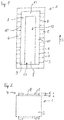
- FIG. 1 shows a plan view of an electrical component. 1
- FIG. 2 shows a cross section of the device FIG. 1 ,
- the electrical component 1 is preferably a piezoelectric component, in particular a piezoelectric actuator.
- the component 1 is designed as a multilayer component.
- the component 1 has a main body 2, in which first and second internal electrodes 3, 4 and functional layers 5 are alternately stacked along a stacking direction S.
- the inner electrodes 3, 4 extend alternately to an outer side 6 of the main body 2 and are spaced from an opposite outer side (not shown).
- the internal electrodes 3, 4 contain copper, silver, or silver-palladium.
- the functional layers 5 are formed, for example, as dielectric layers, in particular as piezoelectric layers.
- the functional layers 5 may be formed of a ceramic material, in particular be formed as piezoceramic layers.
- the device 1 expands upon application of a voltage between the internal electrodes 3, 4. The expansion takes place, for example, in the stacking direction S.
- an external contact 7 is arranged on an outer side 6 of the main body 2.
- the external contact 7 has a first metallization 8 and a second metallization 9.
- the first metallization 8 is in direct contact with the functional layers 5 and the first internal electrodes 3.
- the second metallization 9 is arranged on the first metallization 8 and is in direct contact with the first metallization 8.
- the metallizations 8, 9 are formed in layers.
- the second metallization 9 covers the outside of the first metallization 8, on which it is arranged, that is, the side facing away from the base 2 outside of the first metallization 8, only partially and leaves portions of the outside of the first metallization 8 uncovered.
- Both metallizations 8, 9 are designed as Einbrandmetallmaschineen.
- the metallizations 8, 9 are produced by applying and baking a metallic paste.
- the first metallization 8 is first applied and baked, for example by screen printing.
- the second metallization 9, for example by screen printing, applied and baked.
- Both metallizations 8, 9 contain a metal.
- at least one of the metallizations 8, 9 contains copper.
- the metallizations 8, 9 may contain silver or silver-palladium.
- the metallizations 8, 9 may also contain different metals.
- one of the metallizations may contain copper and the other metallization silver.
- the first metallization 8 contains a glass component, in particular a glass frit.
- the glass content preferably ensures the adhesion of the metallization 8 on the outside 6 of the main body 2, for example on a ceramic material of the main body 2.
- the glass content in the first metallization 8 is between 3 and 10 weight percent (wt .-%).
- the glass content is 6 wt .-%.
- the glass content in the first metallization 8 has the consequence that the wettability of the first metallization 8 with a solder material is low.
- the second metallization 9 has no glass content or has a smaller glass content than the first metallization 8.
- a small proportion of glass from the first metallization 8 can diffuse into the second metallization 9, so that even if a paste without glass content is used to produce the second metallization 9, a small amount of glass after burning in the second Metallization 9 may be present.
- the first metallization 8 may have a higher porosity than the second metallization 9.
- the second metallization 9 is made of a metal.
- the second metallization 9 has a good wettability with a solder material due to the lack of or low glass content.
- the first metallization 8 is in the form of a rectangular area.
- the first metallization 8 has no recesses, so it is formed over its entire surface.
- the second metallization 9 has two strip-shaped subregions 10, 11 which run parallel to one another.
- the partial regions 10, 11 extend in the stacking direction S. Between the partial regions 10, 11, the second metallization 9 has a recess 12, through which the first metallization 8 can be seen.
- the two partial areas 10, 11 are connected to one another by a third partial area 13.
- the third subregion 13 runs perpendicular to the stacking direction S.
- the second metallization 9 is in total U-shaped.
- the second metallization 9 is frame-shaped, wherein an opening 17 is provided in the frame shape.
- the first metallization 8 in the baked state preferably has a thickness d 1 (see FIG. 2 ) in the range of 5 microns to 30 microns.
- the thickness d 1 is 20 microns.
- the second metallization 9 has, for example, a thickness d 2 (see FIG. 2 ) in the range of 10 .mu.m to 60 .mu.m.
- the thickness d 2 is 40 microns.
- the thicknesses d 1 and d 2 may also be the same. For example, both thicknesses d 1 , d 2 can be 20 ⁇ m.
- the area of the first metallization 8 is greater than the area of the second metallization 9. Due to the large area of the first metallization 8, good adhesion of the external contact 7 to the outside 6 can be ensured. Due to the smaller area of the second metallization 9, a contact element in a smaller attachment area the second metallization 9 are attached. Due to the different degree of wettability of the first and second metallization 8, 9, a contact element can be attached in a simple manner only to the second metallization 8 and not, or only to a slight degree, to the first metallization 9. This allows, for example, an attachment of the contact element only in the second metallization 9 defined attachment areas.
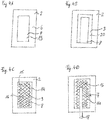
- FIG. 3 shows a plan view of an electrical component 1 with a contact element 14th
- the electrical component 1 is like that in the Figures 1 and 2 formed component, wherein the external contact 7 additionally has a contact element 14 which is arranged on the second metallization 9 here.
- the inner electrodes are not shown here for reasons of clarity.
- the contact element 14 has a net-like structure, in particular a fabric structure.
- the contact element 14 has a plurality of interwoven metallic wires.
- the contact element 14 is soldered to the second metallization 9. Due to the different wettability of the first and second metallization 8, 9 with a solder material, the solder material adheres well to the second metallization 9, but poorly or not at all to the first metallization 8. Thus, a mounting portion 15, in which the contact element 14 with the underlying metallization 8, 9 is determined by the geometry of the second metallization 9. Thus, for soldering the contact element 14 in the contact region 15, a solder material over a large area on the contact element 14 or the Metallizations 8, 9 be applied. Due to the good wettability of the second metallization 9, the contact element 14 is firmly connected to the second metallization 9 by the solder material.
- the contact element 14 Due to the poor wettability of the first metallization 8, the contact element 14 is not connected or only with low adhesion to the first metallization 8. Thus, the contact element 14 can be fastened in a simple manner only in a desired attachment region 15. In particular, the contact element 14 may be only partially, that is attached only in parts of its outer surface, while in a region of low adhesion 16, the contact element 14 is not connected or only with low adhesion 16 to the base body 2. This allows, for example, the electrical bridging of cracks in the main body 2, which can occur during a polarization of the device 1 or during operation.
- the contact element 14 is flexible, so that it occurs when mechanical stresses occur, the z. B. generated by a crack in the body 2, is stretched without tearing.
- a further contact 18 for example a contact pin, can be attached to the external contact 7 (see FIG Figure 4D ).
- the further contact 18 extends beyond the opening 17 into the frame shape of the second metallization 9.
- the further contact 18 is not arranged in an area above the second metallization 9.
- FIGS. 1 to 3 shown component 1.
- a basic body 2 of a component 1 is provided.
- a first metallic paste 19 is applied, for example in a screen printing process, to form a first metallization.
- the first metallic paste 19 is applied in the form of a full-surface filled rectangle.
- the first metallic paste 19 contains a metal, such as copper, and a glass portion. Subsequently, the first metallic paste 19 is baked.
- the burn-in step takes place at a temperature of 760 ° C. in an N 2 atmosphere.
- first metallization 8 is according to FIG. 4B to form the second metallization 9, a second metallic paste 20 is applied, for example in a screen printing process.
- the second metallic paste 8 is U-shaped.
- the second metallic paste 8 contains a metal, for example copper, but no glass component.
- the second metallic paste 20 is baked. For example, the firing step also takes place at 760 ° C.
- One or more further, thin metallic layers are optionally applied to the obtained second metallization 9.
- These layers can be designed to protect the second metallization 9, in particular in the case of a copper having second metallization 9.
- the layers are sputtered on.
- a copper layer and above a silver layer on the second metallization 9 are applied.
- the copper layer is for example, 0.3 microns thick and the silver layer 0.4 microns thick.
- the silver layer preferably dissolves in a solder material.
- a contact element 14 is arranged above the first and second metallization 8, 9.
- the contact element 14 is formed for example as wire mesh.
- the contact element 14 may already be provided with a solder material before being arranged on the main body 2.
- the contact element 14 is galvanized with the solder material.
- the contact element 14 may be provided with solder material on its entire surface facing the main body 2.
- the contact element 14 Due to the poor wettability of the first metallization 9 with the solder material, the contact element 14 is not connected to the first metallization 8 or only with low adhesion strength. Thus, a region of low adhesion strength 16 is formed in a region above the first metallization 8, which is not covered by the second metallization 9.
- the contact element 14 When soldering the contact element 14, the contact element 14 is preferably pressed against the base body 2. Characterized in that the second metallization 9 is arranged on the first metallization 8 and thus a step between the first and second metallization 8, 9 is formed, the contact pressure on the second metallization 9 is higher than on the first metallization 8. Due to the different contact pressure, the different adhesive strength of the contact element on the second metallization 9 is additionally supported.
- the outer geometric dimension of the contact element 14 is preferably slightly smaller than the outer dimension of the second metallization 9.
- the contact element 14 does not protrude laterally beyond the second metallization 9.
- lateral edge regions of the contact element 14 are soldered to the second metallization 9.
- the reliability of the device 1 can be increased.
- it can be prevented that protruding areas of the contact element 14 are damaged, lead to the detachment of the contact element 14 or lead to a short circuit.
- a further contact 18 can be attached to the outer contact 7.
- the RotherWallet réelle 18 may be formed as a contact pin.
- the RotherWallet réelle 18 is placed on the contact element 14 and welded, for example, with the contact element 14.
- the further contact 18 extends through the opening 17 of the second metallization 9 into a central region above the U-shaped second metallization 9. With such an arrangement of the further contact 18, the further contact 18 can be fastened particularly reliably to the contact element 16. In the welding process, the further contact 18 can be pressed against the contact element 14, wherein by the flexibility of the Contact element 14 in the region of low adhesion 16 good contact between the further contact 18 and the contact element 14 can be made. Furthermore, with an arrangement of the further contact 18 such that the contact pin is not arranged above the second metallization 9, the risk of damage to the external contact 7 during the welding process is reduced. In addition, a further contact 18 arranged in this way does not impair or only slightly affect an expansion of the component 1.
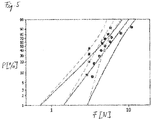
- FIG. 5 shows a diagram in which the frequency P of a deduction of various external contacts against an applied force F is shown.
- a deduction of an external contact falls, for example, a crack of a Jerusalemerressmaschine, a partial detachment of a metallization or a replacement ofmannerWallet réelle of the metallization.
- a device 1 according to FIG. 3 comprising a further contacting 18 in the form of a wire mesh.
- the second metallization 9 was taped with Kapton foil, so that in this area the further contacting 18 was not soldered to the second metallization 9. Subsequently, the non-soldered piece of further contact 18 was attacked during the withdrawal test while exerting various forces. The speed at peeling was 12.5 mm / min.
- the same test was performed with a device 1 in which the first metallization 8 is U-shaped, that is not as in the FIG. 3 the component 1 shown is formed over the entire surface in the form of a rectangle
- the measured values for a full-surface first metallization 8 are represented by circular symbols.
- a Weibull distribution is adjusted, which is represented by dashed lines.
- the measured values for a U-shaped first metallization 8 are represented by the rectangular symbols.
- a Weibull distribution is adjusted, which is represented by solid lines.
- the pull-off average for a full-face first metallization 8 was 5.7 N with a standard deviation of 2.4 N. For a force F of 5.6 N, this was 50% and for a force of 8.2 N was in 90% of cases the external contact 7 deducted.
- the pull-off average for a U-shaped first metallization 8 was 4.1 N with a standard deviation of 1.2 N. For a force F of 4.1 N, 50% and a force of 5.6 N In 90% of cases the external contact 7 had been deducted.
Landscapes
- Engineering & Computer Science (AREA)
- Manufacturing & Machinery (AREA)
- Physics & Mathematics (AREA)
- Electromagnetism (AREA)
- Electric Connection Of Electric Components To Printed Circuits (AREA)
- Connections Effected By Soldering, Adhesion, Or Permanent Deformation (AREA)
- Contacts (AREA)
- Piezo-Electric Or Mechanical Vibrators, Or Delay Or Filter Circuits (AREA)
Claims (15)
- Composant électrique (1), réalisé sous la forme d'un composant multicouche comportant des couches fonctionnelles (5) et des électrodes intérieures (3, 4) disposées entre celles-ci, comportant au moins un contact extérieur (7) présentant une première métallisation (8) et une deuxième métallisation (9), qui est disposée sur la première métallisation (8), dans lequel les première et deuxième métallisations (8, 9) sont cuites, dans lequel la deuxième métallisation (9) ne recouvre qu'en partie la première métallisation (8),
caractérisé en ce que la deuxième métallisation (9) est réalisée en forme de U. - Composant électrique selon la revendication 1, dans lequel les première et deuxième métallisations (8, 9) présentent des mouillabilités différentes avec un matériau de brasage.
- Composant électrique selon l'une des revendications précédentes, dans lequel la première métallisation (8) présente une fraction de verre et dans lequel la deuxième métallisation (9) ne présente aucune fraction de verre ou présente une fraction de verre inférieure à celle de la première métallisation (8) .
- Composant électrique selon l'une des revendications précédentes, dans lequel la deuxième métallisation (9) présente au moins un évidement (12).
- Composant électrique selon la revendication 4, dans lequel la première métallisation (8) se trouve dans l'évidement (12).
- Composant électrique selon l'une des revendications précédentes, dans lequel la première métallisation (8) est réalisée de manière à s'étendre sur la totalité de la surface.
- Composant électrique selon l'une des revendications précédentes, dans lequel un élément de contact (14) est fixé à la deuxième métallisation (9).
- Composant électrique selon la revendication 7, dans lequel l'élément de contact (14) est brasé.
- Composant électrique selon l'une des revendications 7 ou 8, dans lequel l'élément de contact (14) présente une structure de tissu.
- Composant électrique selon l'une des revendications 7 à 9, comportant un prolongateur de contact (18) qui est fixé à l'élément de contact (14).
- Composant électrique selon la revendication 10, dans lequel le prolongateur de contact (18) n'est pas disposé au-dessus de la deuxième métallisation (9).
- Composant électrique selon l'une des revendications 10 ou 11, dans lequel le prolongement de contact (18) s'étend au-dessus d'une ouverture (17) de la forme en U à l'intérieur de la forme en U.
- Composant électrique selon l'une des revendications 10 à 12, dans lequel le prolongement de contact (18) est réalisé sous la forme d'une broche de contact.
- Composant électrique selon l'une des revendications précédentes, qui est réalisé sous la forme d'un actionneur piézoélectrique.
- Procédé d'établissement d'un contact électrique d'un composant électrique selon l'une des revendications précédentes, comportant les étapes consistant à :A) fournir un corps de base (2) du composant électrique (1) et déposer une première pâte métallique (19) sur une face extérieure (6) du corps de base (2),B) cuire la première pâte métallique (19) pour former la première métallisation (8),C) déposer une deuxième pâte métallique (20) sur la première métallisation (8),D) cuire la deuxième pâte métallique (20) pour former la deuxième métallisation (9).
Applications Claiming Priority (2)
| Application Number | Priority Date | Filing Date | Title |
|---|---|---|---|
| DE102012109250.8A DE102012109250B4 (de) | 2012-09-28 | 2012-09-28 | Elektrisches Bauelement und Verfahren zur Herstellung einer Kontaktierung eines Elektrischen Bauelements |
| PCT/EP2013/068633 WO2014048713A2 (fr) | 2012-09-28 | 2013-09-09 | Composant électrique et procédé d'établissement d'une mise en contact électrique d'un composant électrique |
Publications (2)
| Publication Number | Publication Date |
|---|---|
| EP2901504A2 EP2901504A2 (fr) | 2015-08-05 |
| EP2901504B1 true EP2901504B1 (fr) | 2018-08-15 |
Family
ID=49165729
Family Applications (1)
| Application Number | Title | Priority Date | Filing Date |
|---|---|---|---|
| EP13762093.6A Active EP2901504B1 (fr) | 2012-09-28 | 2013-09-09 | Composant électrique et procédé d'établissement d'une mise en contact électrique d'un composant électrique |
Country Status (6)
| Country | Link |
|---|---|
| US (1) | US9613773B2 (fr) |
| EP (1) | EP2901504B1 (fr) |
| JP (2) | JP6486273B2 (fr) |
| CN (1) | CN104662685B (fr) |
| DE (1) | DE102012109250B4 (fr) |
| WO (1) | WO2014048713A2 (fr) |
Families Citing this family (2)
| Publication number | Priority date | Publication date | Assignee | Title |
|---|---|---|---|---|
| US10658565B2 (en) * | 2016-08-29 | 2020-05-19 | The Boeing Company | Actuator assemblies, mechanical assemblies including the actuator assemblies, and methods of fabricating the same |
| US11296272B2 (en) * | 2017-07-20 | 2022-04-05 | Taiyo Yuden Co., Ltd. | Multilayer piezoelectric element, piezoelectric vibration apparatus, and electronic device |
Family Cites Families (24)
| Publication number | Priority date | Publication date | Assignee | Title |
|---|---|---|---|---|
| JPS63120450A (ja) * | 1986-11-10 | 1988-05-24 | Shinko Electric Ind Co Ltd | 半導体装置の製造方法およびこれに用いるリ−ドフレ−ム |
| DE19648545B4 (de) | 1996-11-25 | 2009-05-07 | Ceramtec Ag | Monolithischer Vielschichtaktor mit Außenelektroden |
| DE19917728A1 (de) * | 1999-04-20 | 2000-10-26 | Bosch Gmbh Robert | Piezoelektrischer Aktor |
| DE60103445T2 (de) * | 2000-03-29 | 2005-06-02 | Nec Tokin Ceramics Corp. | Vielschicht-Piezoaktor mit Elektroden mit verstärkter Leitfähigkeit |
| US20010033125A1 (en) * | 2000-04-20 | 2001-10-25 | Tokin Corporation | Multilayer piezoelectric actuator device having a conductive member attached to an external electrode thereof |
| JP3964184B2 (ja) * | 2000-12-28 | 2007-08-22 | 株式会社デンソー | 積層型圧電アクチュエータ |
| DE10327902A1 (de) | 2002-07-19 | 2004-06-24 | Ceramtec Ag Innovative Ceramic Engineering | Außenelektrode an einem piezokeramischen Vielschichtaktor |
| DE10356961A1 (de) * | 2003-12-05 | 2005-06-30 | Robert Bosch Gmbh | Aktormodul |
| US7385337B2 (en) * | 2004-06-18 | 2008-06-10 | Tdk Corporation | Multilayer piezoelectric element |
| JP4706209B2 (ja) * | 2004-08-30 | 2011-06-22 | 株式会社デンソー | 積層型圧電体素子及びその製造方法並びに導電性接着剤 |
| JP2006303045A (ja) * | 2005-04-18 | 2006-11-02 | Denso Corp | 積層型圧電体素子 |
| EP2003707B1 (fr) * | 2006-03-31 | 2012-03-14 | Murata Manufacturing Co. Ltd. | Actionneur piezo-electrique |
| JP5087914B2 (ja) * | 2006-12-06 | 2012-12-05 | Tdk株式会社 | 積層型圧電素子 |
| JP2008243924A (ja) * | 2007-03-26 | 2008-10-09 | Ngk Spark Plug Co Ltd | 積層型圧電アクチュエータ素子及び積層型圧電アクチュエータ |
| JP2009123750A (ja) * | 2007-11-12 | 2009-06-04 | Denso Corp | 積層型圧電素子 |
| KR20100138931A (ko) | 2008-03-21 | 2010-12-31 | 엔지케이 인슐레이터 엘티디 | 압전/전왜 소자 및 그 제조 방법 |
| EP2259352B1 (fr) * | 2008-04-11 | 2012-08-29 | Murata Manufacturing Co. Ltd. | Actionneur piézo-électrique laminé |
| DE102008062021A1 (de) | 2008-08-18 | 2010-03-04 | Epcos Ag | Piezoaktor in Vielschichtbauweise |
| CN102132432A (zh) * | 2008-08-26 | 2011-07-20 | 京瓷株式会社 | 层叠型压电元件及使用该层叠型压电元件的喷射装置以及燃料喷射系统 |
| US8991723B2 (en) | 2009-05-26 | 2015-03-31 | Kyocera Corporation | Multi-layer piezoelectric element, and injection device and fuel injection system incorporating the multi-layer piezoelectric element |
| JP5421373B2 (ja) * | 2009-07-28 | 2014-02-19 | 京セラ株式会社 | 積層型圧電素子およびこれを用いた噴射装置ならびに燃料噴射システム |
| CN103098251B (zh) * | 2010-10-28 | 2015-04-01 | 京瓷株式会社 | 层叠型压电元件以及使用其的喷射装置和燃料喷射系统 |
| CN104350624B (zh) * | 2012-10-29 | 2017-04-05 | 京瓷株式会社 | 层叠型压电元件及具备其的压电致动器、喷射装置以及燃料喷射系统 |
| JP6185608B2 (ja) * | 2014-01-30 | 2017-08-23 | 京セラ株式会社 | 積層型圧電素子およびこれを備えた噴射装置ならびに燃料噴射システム |
-
2012
- 2012-09-28 DE DE102012109250.8A patent/DE102012109250B4/de active Active
-
2013
- 2013-09-09 US US14/431,726 patent/US9613773B2/en active Active
- 2013-09-09 EP EP13762093.6A patent/EP2901504B1/fr active Active
- 2013-09-09 CN CN201380050759.4A patent/CN104662685B/zh active Active
- 2013-09-09 WO PCT/EP2013/068633 patent/WO2014048713A2/fr not_active Ceased
- 2013-09-09 JP JP2015533517A patent/JP6486273B2/ja active Active
-
2017
- 2017-07-14 JP JP2017138300A patent/JP6629796B2/ja active Active
Non-Patent Citations (1)
| Title |
|---|
| None * |
Also Published As
| Publication number | Publication date |
|---|---|
| WO2014048713A2 (fr) | 2014-04-03 |
| EP2901504A2 (fr) | 2015-08-05 |
| WO2014048713A3 (fr) | 2014-06-05 |
| CN104662685B (zh) | 2017-08-15 |
| CN104662685A (zh) | 2015-05-27 |
| US20150255237A1 (en) | 2015-09-10 |
| DE102012109250A1 (de) | 2014-04-03 |
| JP2015531548A (ja) | 2015-11-02 |
| JP6629796B2 (ja) | 2020-01-15 |
| JP6486273B2 (ja) | 2019-03-20 |
| JP2017201714A (ja) | 2017-11-09 |
| DE102012109250B4 (de) | 2020-07-16 |
| US9613773B2 (en) | 2017-04-04 |
Similar Documents
| Publication | Publication Date | Title |
|---|---|---|
| EP2316142B1 (fr) | Actionneur piézoélectrique de conception multicouche | |
| EP3371565B1 (fr) | Élément capteur et procédé de fabrication d'un élément capteur | |
| EP2057647B1 (fr) | Ensemble composant | |
| EP2011170B1 (fr) | Procédé de production d'un actionneur piézo | |
| EP2345095B1 (fr) | Actionneur piézoélectrique de construction multicouche et procédé de fixation d'une électrode extérieure sur un actionneur piézoélectrique | |
| DE3638286A1 (de) | Elektrisches bauelement aus keramik mit mehrlagenmetallisierung und verfahren zu seiner herstellung | |
| DE102004031878B3 (de) | Elektrisches Mehrschichtbauelement mit zuverlässigem Lötkontakt | |
| DE102004006778A1 (de) | Gestapelte piezoelektrische Vorrichtung | |
| EP2901504B1 (fr) | Composant électrique et procédé d'établissement d'une mise en contact électrique d'un composant électrique | |
| EP3033756B1 (fr) | Procede de fabrication d'un composant multicouche comportant un element de mise en contact exterieur | |
| DE102010022925B4 (de) | Piezoelektrisches Vielschichtbauelement und Verfahren zur Ausbildung einer Außenelektrode bei einem piezoelektrischen Vielschichtbauelement | |
| EP1774543B1 (fr) | Composant électrique et procédé pour produire un composant électrique | |
| DE19635276C2 (de) | Elektro-keramisches Vielschichtbauelement und Verfahren zu seiner Herstellung | |
| EP1714328A2 (fr) | Actionneur piezo-electrique et procede de production correspondant | |
| DE102012105517B4 (de) | Vielschichtbauelement mit einer Außenkontaktierung und Verfahren zur Herstellung eines Vielschichtbauelements mit einer Außenkontaktierung | |
| DE102012110556B4 (de) | Vielschichtbauelement und Verfahren zu dessen Herstellung | |
| DE102014217938B4 (de) | Elektronisches Bauelement | |
| DE102018123594B4 (de) | Verfahren zur Herstellung eines keramischen Bauelements | |
| DE19634488A1 (de) | Elektro-keramisches Bauelement und Verfahren zu seiner Herstellung | |
| WO2020064403A1 (fr) | Composant en céramique et son procédé de fabrication |
Legal Events
| Date | Code | Title | Description |
|---|---|---|---|
| PUAI | Public reference made under article 153(3) epc to a published international application that has entered the european phase |
Free format text: ORIGINAL CODE: 0009012 |
|
| 17P | Request for examination filed |
Effective date: 20150209 |
|
| AK | Designated contracting states |
Kind code of ref document: A2 Designated state(s): AL AT BE BG CH CY CZ DE DK EE ES FI FR GB GR HR HU IE IS IT LI LT LU LV MC MK MT NL NO PL PT RO RS SE SI SK SM TR |
|
| AX | Request for extension of the european patent |
Extension state: BA ME |
|
| DAX | Request for extension of the european patent (deleted) | ||
| RAP1 | Party data changed (applicant data changed or rights of an application transferred) |
Owner name: EPCOS AG |
|
| GRAP | Despatch of communication of intention to grant a patent |
Free format text: ORIGINAL CODE: EPIDOSNIGR1 |
|
| INTG | Intention to grant announced |
Effective date: 20180508 |
|
| GRAS | Grant fee paid |
Free format text: ORIGINAL CODE: EPIDOSNIGR3 |
|
| GRAA | (expected) grant |
Free format text: ORIGINAL CODE: 0009210 |
|
| AK | Designated contracting states |
Kind code of ref document: B1 Designated state(s): AL AT BE BG CH CY CZ DE DK EE ES FI FR GB GR HR HU IE IS IT LI LT LU LV MC MK MT NL NO PL PT RO RS SE SI SK SM TR |
|
| REG | Reference to a national code |
Ref country code: CH Ref legal event code: EP Ref country code: GB Ref legal event code: FG4D Free format text: NOT ENGLISH Ref country code: AT Ref legal event code: REF Ref document number: 1030779 Country of ref document: AT Kind code of ref document: T Effective date: 20180815 |
|
| REG | Reference to a national code |
Ref country code: IE Ref legal event code: FG4D Free format text: LANGUAGE OF EP DOCUMENT: GERMAN |
|
| REG | Reference to a national code |
Ref country code: DE Ref legal event code: R096 Ref document number: 502013010879 Country of ref document: DE |
|
| REG | Reference to a national code |
Ref country code: DE Ref legal event code: R082 Ref document number: 502013010879 Country of ref document: DE Representative=s name: EPPING HERMANN FISCHER PATENTANWALTSGESELLSCHA, DE Ref country code: DE Ref legal event code: R081 Ref document number: 502013010879 Country of ref document: DE Owner name: TDK ELECTRONICS AG, DE Free format text: FORMER OWNER: EPCOS AG, 81671 MUENCHEN, DE |
|
| REG | Reference to a national code |
Ref country code: NL Ref legal event code: MP Effective date: 20180815 |
|
| REG | Reference to a national code |
Ref country code: LT Ref legal event code: MG4D |
|
| PG25 | Lapsed in a contracting state [announced via postgrant information from national office to epo] |
Ref country code: GR Free format text: LAPSE BECAUSE OF FAILURE TO SUBMIT A TRANSLATION OF THE DESCRIPTION OR TO PAY THE FEE WITHIN THE PRESCRIBED TIME-LIMIT Effective date: 20181116 Ref country code: SE Free format text: LAPSE BECAUSE OF FAILURE TO SUBMIT A TRANSLATION OF THE DESCRIPTION OR TO PAY THE FEE WITHIN THE PRESCRIBED TIME-LIMIT Effective date: 20180815 Ref country code: BG Free format text: LAPSE BECAUSE OF FAILURE TO SUBMIT A TRANSLATION OF THE DESCRIPTION OR TO PAY THE FEE WITHIN THE PRESCRIBED TIME-LIMIT Effective date: 20181115 Ref country code: NL Free format text: LAPSE BECAUSE OF FAILURE TO SUBMIT A TRANSLATION OF THE DESCRIPTION OR TO PAY THE FEE WITHIN THE PRESCRIBED TIME-LIMIT Effective date: 20180815 Ref country code: LT Free format text: LAPSE BECAUSE OF FAILURE TO SUBMIT A TRANSLATION OF THE DESCRIPTION OR TO PAY THE FEE WITHIN THE PRESCRIBED TIME-LIMIT Effective date: 20180815 Ref country code: FI Free format text: LAPSE BECAUSE OF FAILURE TO SUBMIT A TRANSLATION OF THE DESCRIPTION OR TO PAY THE FEE WITHIN THE PRESCRIBED TIME-LIMIT Effective date: 20180815 Ref country code: RS Free format text: LAPSE BECAUSE OF FAILURE TO SUBMIT A TRANSLATION OF THE DESCRIPTION OR TO PAY THE FEE WITHIN THE PRESCRIBED TIME-LIMIT Effective date: 20180815 Ref country code: IS Free format text: LAPSE BECAUSE OF FAILURE TO SUBMIT A TRANSLATION OF THE DESCRIPTION OR TO PAY THE FEE WITHIN THE PRESCRIBED TIME-LIMIT Effective date: 20181215 Ref country code: NO Free format text: LAPSE BECAUSE OF FAILURE TO SUBMIT A TRANSLATION OF THE DESCRIPTION OR TO PAY THE FEE WITHIN THE PRESCRIBED TIME-LIMIT Effective date: 20181115 |
|
| PG25 | Lapsed in a contracting state [announced via postgrant information from national office to epo] |
Ref country code: AL Free format text: LAPSE BECAUSE OF FAILURE TO SUBMIT A TRANSLATION OF THE DESCRIPTION OR TO PAY THE FEE WITHIN THE PRESCRIBED TIME-LIMIT Effective date: 20180815 Ref country code: HR Free format text: LAPSE BECAUSE OF FAILURE TO SUBMIT A TRANSLATION OF THE DESCRIPTION OR TO PAY THE FEE WITHIN THE PRESCRIBED TIME-LIMIT Effective date: 20180815 Ref country code: LV Free format text: LAPSE BECAUSE OF FAILURE TO SUBMIT A TRANSLATION OF THE DESCRIPTION OR TO PAY THE FEE WITHIN THE PRESCRIBED TIME-LIMIT Effective date: 20180815 |
|
| PG25 | Lapsed in a contracting state [announced via postgrant information from national office to epo] |
Ref country code: RO Free format text: LAPSE BECAUSE OF FAILURE TO SUBMIT A TRANSLATION OF THE DESCRIPTION OR TO PAY THE FEE WITHIN THE PRESCRIBED TIME-LIMIT Effective date: 20180815 Ref country code: IT Free format text: LAPSE BECAUSE OF FAILURE TO SUBMIT A TRANSLATION OF THE DESCRIPTION OR TO PAY THE FEE WITHIN THE PRESCRIBED TIME-LIMIT Effective date: 20180815 Ref country code: EE Free format text: LAPSE BECAUSE OF FAILURE TO SUBMIT A TRANSLATION OF THE DESCRIPTION OR TO PAY THE FEE WITHIN THE PRESCRIBED TIME-LIMIT Effective date: 20180815 Ref country code: ES Free format text: LAPSE BECAUSE OF FAILURE TO SUBMIT A TRANSLATION OF THE DESCRIPTION OR TO PAY THE FEE WITHIN THE PRESCRIBED TIME-LIMIT Effective date: 20180815 Ref country code: CZ Free format text: LAPSE BECAUSE OF FAILURE TO SUBMIT A TRANSLATION OF THE DESCRIPTION OR TO PAY THE FEE WITHIN THE PRESCRIBED TIME-LIMIT Effective date: 20180815 Ref country code: PL Free format text: LAPSE BECAUSE OF FAILURE TO SUBMIT A TRANSLATION OF THE DESCRIPTION OR TO PAY THE FEE WITHIN THE PRESCRIBED TIME-LIMIT Effective date: 20180815 |
|
| REG | Reference to a national code |
Ref country code: CH Ref legal event code: PL |
|
| REG | Reference to a national code |
Ref country code: DE Ref legal event code: R097 Ref document number: 502013010879 Country of ref document: DE |
|
| PG25 | Lapsed in a contracting state [announced via postgrant information from national office to epo] |
Ref country code: SK Free format text: LAPSE BECAUSE OF FAILURE TO SUBMIT A TRANSLATION OF THE DESCRIPTION OR TO PAY THE FEE WITHIN THE PRESCRIBED TIME-LIMIT Effective date: 20180815 Ref country code: DK Free format text: LAPSE BECAUSE OF FAILURE TO SUBMIT A TRANSLATION OF THE DESCRIPTION OR TO PAY THE FEE WITHIN THE PRESCRIBED TIME-LIMIT Effective date: 20180815 Ref country code: SM Free format text: LAPSE BECAUSE OF FAILURE TO SUBMIT A TRANSLATION OF THE DESCRIPTION OR TO PAY THE FEE WITHIN THE PRESCRIBED TIME-LIMIT Effective date: 20180815 |
|
| REG | Reference to a national code |
Ref country code: BE Ref legal event code: MM Effective date: 20180930 |
|
| PLBE | No opposition filed within time limit |
Free format text: ORIGINAL CODE: 0009261 |
|
| STAA | Information on the status of an ep patent application or granted ep patent |
Free format text: STATUS: NO OPPOSITION FILED WITHIN TIME LIMIT |
|
| REG | Reference to a national code |
Ref country code: IE Ref legal event code: MM4A |
|
| PG25 | Lapsed in a contracting state [announced via postgrant information from national office to epo] |
Ref country code: LU Free format text: LAPSE BECAUSE OF NON-PAYMENT OF DUE FEES Effective date: 20180909 Ref country code: MC Free format text: LAPSE BECAUSE OF FAILURE TO SUBMIT A TRANSLATION OF THE DESCRIPTION OR TO PAY THE FEE WITHIN THE PRESCRIBED TIME-LIMIT Effective date: 20180815 |
|
| 26N | No opposition filed |
Effective date: 20190516 |
|
| GBPC | Gb: european patent ceased through non-payment of renewal fee |
Effective date: 20181115 |
|
| PG25 | Lapsed in a contracting state [announced via postgrant information from national office to epo] |
Ref country code: IE Free format text: LAPSE BECAUSE OF NON-PAYMENT OF DUE FEES Effective date: 20180909 |
|
| PG25 | Lapsed in a contracting state [announced via postgrant information from national office to epo] |
Ref country code: FR Free format text: LAPSE BECAUSE OF NON-PAYMENT OF DUE FEES Effective date: 20181015 Ref country code: LI Free format text: LAPSE BECAUSE OF NON-PAYMENT OF DUE FEES Effective date: 20180930 Ref country code: CH Free format text: LAPSE BECAUSE OF NON-PAYMENT OF DUE FEES Effective date: 20180930 Ref country code: SI Free format text: LAPSE BECAUSE OF FAILURE TO SUBMIT A TRANSLATION OF THE DESCRIPTION OR TO PAY THE FEE WITHIN THE PRESCRIBED TIME-LIMIT Effective date: 20180815 Ref country code: BE Free format text: LAPSE BECAUSE OF NON-PAYMENT OF DUE FEES Effective date: 20180930 |
|
| REG | Reference to a national code |
Ref country code: AT Ref legal event code: MM01 Ref document number: 1030779 Country of ref document: AT Kind code of ref document: T Effective date: 20180909 |
|
| PG25 | Lapsed in a contracting state [announced via postgrant information from national office to epo] |
Ref country code: GB Free format text: LAPSE BECAUSE OF NON-PAYMENT OF DUE FEES Effective date: 20181115 |
|
| PG25 | Lapsed in a contracting state [announced via postgrant information from national office to epo] |
Ref country code: AT Free format text: LAPSE BECAUSE OF NON-PAYMENT OF DUE FEES Effective date: 20180909 Ref country code: MT Free format text: LAPSE BECAUSE OF FAILURE TO SUBMIT A TRANSLATION OF THE DESCRIPTION OR TO PAY THE FEE WITHIN THE PRESCRIBED TIME-LIMIT Effective date: 20180815 |
|
| PG25 | Lapsed in a contracting state [announced via postgrant information from national office to epo] |
Ref country code: TR Free format text: LAPSE BECAUSE OF FAILURE TO SUBMIT A TRANSLATION OF THE DESCRIPTION OR TO PAY THE FEE WITHIN THE PRESCRIBED TIME-LIMIT Effective date: 20180815 |
|
| PG25 | Lapsed in a contracting state [announced via postgrant information from national office to epo] |
Ref country code: PT Free format text: LAPSE BECAUSE OF FAILURE TO SUBMIT A TRANSLATION OF THE DESCRIPTION OR TO PAY THE FEE WITHIN THE PRESCRIBED TIME-LIMIT Effective date: 20180815 |
|
| PG25 | Lapsed in a contracting state [announced via postgrant information from national office to epo] |
Ref country code: HU Free format text: LAPSE BECAUSE OF FAILURE TO SUBMIT A TRANSLATION OF THE DESCRIPTION OR TO PAY THE FEE WITHIN THE PRESCRIBED TIME-LIMIT; INVALID AB INITIO Effective date: 20130909 Ref country code: MK Free format text: LAPSE BECAUSE OF NON-PAYMENT OF DUE FEES Effective date: 20180815 Ref country code: CY Free format text: LAPSE BECAUSE OF FAILURE TO SUBMIT A TRANSLATION OF THE DESCRIPTION OR TO PAY THE FEE WITHIN THE PRESCRIBED TIME-LIMIT Effective date: 20180815 |
|
| REG | Reference to a national code |
Ref country code: DE Ref legal event code: R079 Ref document number: 502013010879 Country of ref document: DE Free format text: PREVIOUS MAIN CLASS: H01L0041047000 Ipc: H10N0030870000 |
|
| P01 | Opt-out of the competence of the unified patent court (upc) registered |
Effective date: 20230521 |
|
| PGFP | Annual fee paid to national office [announced via postgrant information from national office to epo] |
Ref country code: DE Payment date: 20250923 Year of fee payment: 13 |