EP2902996A1 - Dispositif d'affichage et procédé de commande de celui-ci - Google Patents
Dispositif d'affichage et procédé de commande de celui-ci Download PDFInfo
- Publication number
- EP2902996A1 EP2902996A1 EP13841236.6A EP13841236A EP2902996A1 EP 2902996 A1 EP2902996 A1 EP 2902996A1 EP 13841236 A EP13841236 A EP 13841236A EP 2902996 A1 EP2902996 A1 EP 2902996A1
- Authority
- EP
- European Patent Office
- Prior art keywords
- image data
- refreshing
- image
- section
- data
- Prior art date
- Legal status (The legal status is an assumption and is not a legal conclusion. Google has not performed a legal analysis and makes no representation as to the accuracy of the status listed.)
- Withdrawn
Links
- 238000000034 method Methods 0.000 title claims description 37
- 238000012937 correction Methods 0.000 claims abstract description 107
- 230000015572 biosynthetic process Effects 0.000 claims description 131
- 238000013500 data storage Methods 0.000 claims description 42
- 230000008859 change Effects 0.000 abstract description 38
- 239000004973 liquid crystal related substance Substances 0.000 description 142
- 238000010586 diagram Methods 0.000 description 24
- 230000007423 decrease Effects 0.000 description 16
- 230000003247 decreasing effect Effects 0.000 description 12
- 230000008901 benefit Effects 0.000 description 11
- 239000004065 semiconductor Substances 0.000 description 8
- 239000000470 constituent Substances 0.000 description 5
- 230000008569 process Effects 0.000 description 5
- 239000010409 thin film Substances 0.000 description 5
- GYHNNYVSQQEPJS-UHFFFAOYSA-N Gallium Chemical compound [Ga] GYHNNYVSQQEPJS-UHFFFAOYSA-N 0.000 description 4
- 229910052733 gallium Inorganic materials 0.000 description 4
- 229910052738 indium Inorganic materials 0.000 description 4
- APFVFJFRJDLVQX-UHFFFAOYSA-N indium atom Chemical compound [In] APFVFJFRJDLVQX-UHFFFAOYSA-N 0.000 description 4
- XUIMIQQOPSSXEZ-UHFFFAOYSA-N Silicon Chemical compound [Si] XUIMIQQOPSSXEZ-UHFFFAOYSA-N 0.000 description 3
- HCHKCACWOHOZIP-UHFFFAOYSA-N Zinc Chemical compound [Zn] HCHKCACWOHOZIP-UHFFFAOYSA-N 0.000 description 3
- QVGXLLKOCUKJST-UHFFFAOYSA-N atomic oxygen Chemical compound [O] QVGXLLKOCUKJST-UHFFFAOYSA-N 0.000 description 3
- 229910052760 oxygen Inorganic materials 0.000 description 3
- 239000001301 oxygen Substances 0.000 description 3
- 229910052710 silicon Inorganic materials 0.000 description 3
- 239000010703 silicon Substances 0.000 description 3
- 229910052725 zinc Inorganic materials 0.000 description 3
- 239000011701 zinc Substances 0.000 description 3
- 229910021417 amorphous silicon Inorganic materials 0.000 description 2
- 239000011575 calcium Substances 0.000 description 2
- 238000006243 chemical reaction Methods 0.000 description 2
- 239000010949 copper Substances 0.000 description 2
- 230000003111 delayed effect Effects 0.000 description 2
- 230000000694 effects Effects 0.000 description 2
- 230000006870 function Effects 0.000 description 2
- OYPRJOBELJOOCE-UHFFFAOYSA-N Calcium Chemical compound [Ca] OYPRJOBELJOOCE-UHFFFAOYSA-N 0.000 description 1
- RYGMFSIKBFXOCR-UHFFFAOYSA-N Copper Chemical compound [Cu] RYGMFSIKBFXOCR-UHFFFAOYSA-N 0.000 description 1
- ATJFFYVFTNAWJD-UHFFFAOYSA-N Tin Chemical compound [Sn] ATJFFYVFTNAWJD-UHFFFAOYSA-N 0.000 description 1
- 229910052782 aluminium Inorganic materials 0.000 description 1
- XAGFODPZIPBFFR-UHFFFAOYSA-N aluminium Chemical compound [Al] XAGFODPZIPBFFR-UHFFFAOYSA-N 0.000 description 1
- 229910052791 calcium Inorganic materials 0.000 description 1
- 238000004364 calculation method Methods 0.000 description 1
- 239000003086 colorant Substances 0.000 description 1
- 238000007796 conventional method Methods 0.000 description 1
- 229910052802 copper Inorganic materials 0.000 description 1
- 238000013461 design Methods 0.000 description 1
- 230000006866 deterioration Effects 0.000 description 1
- 238000011161 development Methods 0.000 description 1
- 229910052732 germanium Inorganic materials 0.000 description 1
- GNPVGFCGXDBREM-UHFFFAOYSA-N germanium atom Chemical compound [Ge] GNPVGFCGXDBREM-UHFFFAOYSA-N 0.000 description 1
- 239000004615 ingredient Substances 0.000 description 1
- 239000011159 matrix material Substances 0.000 description 1
- 229910021424 microcrystalline silicon Inorganic materials 0.000 description 1
- 229910021420 polycrystalline silicon Inorganic materials 0.000 description 1
- 229920005591 polysilicon Polymers 0.000 description 1
- 238000012545 processing Methods 0.000 description 1
- 230000004044 response Effects 0.000 description 1
- 230000009131 signaling function Effects 0.000 description 1
- JBQYATWDVHIOAR-UHFFFAOYSA-N tellanylidenegermanium Chemical compound [Te]=[Ge] JBQYATWDVHIOAR-UHFFFAOYSA-N 0.000 description 1
Images






Classifications
-
- G—PHYSICS
- G09—EDUCATION; CRYPTOGRAPHY; DISPLAY; ADVERTISING; SEALS
- G09G—ARRANGEMENTS OR CIRCUITS FOR CONTROL OF INDICATING DEVICES USING STATIC MEANS TO PRESENT VARIABLE INFORMATION
- G09G5/00—Control arrangements or circuits for visual indicators common to cathode-ray tube indicators and other visual indicators
- G09G5/18—Timing circuits for raster scan displays
-
- G—PHYSICS
- G09—EDUCATION; CRYPTOGRAPHY; DISPLAY; ADVERTISING; SEALS
- G09G—ARRANGEMENTS OR CIRCUITS FOR CONTROL OF INDICATING DEVICES USING STATIC MEANS TO PRESENT VARIABLE INFORMATION
- G09G3/00—Control arrangements or circuits, of interest only in connection with visual indicators other than cathode-ray tubes
- G09G3/20—Control arrangements or circuits, of interest only in connection with visual indicators other than cathode-ray tubes for presentation of an assembly of a number of characters, e.g. a page, by composing the assembly by combination of individual elements arranged in a matrix no fixed position being assigned to or needed to be assigned to the individual characters or partial characters
- G09G3/34—Control arrangements or circuits, of interest only in connection with visual indicators other than cathode-ray tubes for presentation of an assembly of a number of characters, e.g. a page, by composing the assembly by combination of individual elements arranged in a matrix no fixed position being assigned to or needed to be assigned to the individual characters or partial characters by control of light from an independent source
- G09G3/36—Control arrangements or circuits, of interest only in connection with visual indicators other than cathode-ray tubes for presentation of an assembly of a number of characters, e.g. a page, by composing the assembly by combination of individual elements arranged in a matrix no fixed position being assigned to or needed to be assigned to the individual characters or partial characters by control of light from an independent source using liquid crystals
- G09G3/3611—Control of matrices with row and column drivers
- G09G3/3614—Control of polarity reversal in general
-
- G—PHYSICS
- G09—EDUCATION; CRYPTOGRAPHY; DISPLAY; ADVERTISING; SEALS
- G09G—ARRANGEMENTS OR CIRCUITS FOR CONTROL OF INDICATING DEVICES USING STATIC MEANS TO PRESENT VARIABLE INFORMATION
- G09G3/00—Control arrangements or circuits, of interest only in connection with visual indicators other than cathode-ray tubes
- G09G3/20—Control arrangements or circuits, of interest only in connection with visual indicators other than cathode-ray tubes for presentation of an assembly of a number of characters, e.g. a page, by composing the assembly by combination of individual elements arranged in a matrix no fixed position being assigned to or needed to be assigned to the individual characters or partial characters
- G09G3/34—Control arrangements or circuits, of interest only in connection with visual indicators other than cathode-ray tubes for presentation of an assembly of a number of characters, e.g. a page, by composing the assembly by combination of individual elements arranged in a matrix no fixed position being assigned to or needed to be assigned to the individual characters or partial characters by control of light from an independent source
- G09G3/36—Control arrangements or circuits, of interest only in connection with visual indicators other than cathode-ray tubes for presentation of an assembly of a number of characters, e.g. a page, by composing the assembly by combination of individual elements arranged in a matrix no fixed position being assigned to or needed to be assigned to the individual characters or partial characters by control of light from an independent source using liquid crystals
- G09G3/3611—Control of matrices with row and column drivers
-
- G—PHYSICS
- G09—EDUCATION; CRYPTOGRAPHY; DISPLAY; ADVERTISING; SEALS
- G09G—ARRANGEMENTS OR CIRCUITS FOR CONTROL OF INDICATING DEVICES USING STATIC MEANS TO PRESENT VARIABLE INFORMATION
- G09G5/00—Control arrangements or circuits for visual indicators common to cathode-ray tube indicators and other visual indicators
- G09G5/02—Control arrangements or circuits for visual indicators common to cathode-ray tube indicators and other visual indicators characterised by the way in which colour is displayed
-
- G—PHYSICS
- G09—EDUCATION; CRYPTOGRAPHY; DISPLAY; ADVERTISING; SEALS
- G09G—ARRANGEMENTS OR CIRCUITS FOR CONTROL OF INDICATING DEVICES USING STATIC MEANS TO PRESENT VARIABLE INFORMATION
- G09G2310/00—Command of the display device
- G09G2310/02—Addressing, scanning or driving the display screen or processing steps related thereto
- G09G2310/0202—Addressing of scan or signal lines
-
- G—PHYSICS
- G09—EDUCATION; CRYPTOGRAPHY; DISPLAY; ADVERTISING; SEALS
- G09G—ARRANGEMENTS OR CIRCUITS FOR CONTROL OF INDICATING DEVICES USING STATIC MEANS TO PRESENT VARIABLE INFORMATION
- G09G2310/00—Command of the display device
- G09G2310/04—Partial updating of the display screen
-
- G—PHYSICS
- G09—EDUCATION; CRYPTOGRAPHY; DISPLAY; ADVERTISING; SEALS
- G09G—ARRANGEMENTS OR CIRCUITS FOR CONTROL OF INDICATING DEVICES USING STATIC MEANS TO PRESENT VARIABLE INFORMATION
- G09G2330/00—Aspects of power supply; Aspects of display protection and defect management
- G09G2330/02—Details of power systems and of start or stop of display operation
- G09G2330/021—Power management, e.g. power saving
Definitions
- the present invention relates to display devices, and more particularly to a display device which performs intermission driving, and a method of driving the same.
- a liquid crystal display device which performs intermission driving alternately repeats a drive period for scanning lines and writing data voltage thereby refreshing an image, and an intermission period for bringing all the scanning lines into a de-selected state thereby stopping the writing of data voltage.
- a voltage applied to a liquid crystal layer in each pixel formation portion during an immediately preceding drive period (hereinafter called "liquid crystal application voltage") is maintained, so the displayed image is maintained.
- liquid crystal application voltage a voltage applied to a liquid crystal layer in each pixel formation portion during an immediately preceding drive period
- Patent Literature 1 discloses a liquid crystal display device which performs such an intermission driving as described above.
- the liquid crystal display device uses a liquid crystal panel, which is composed of two electrode panels sandwiching a liquid crystal layer in between.
- a voltage is applied to the liquid crystal layer, liquid crystal molecules in the liquid crystal layer change their alignment direction (orientation of the long axis) due to dielectric constant anisotropy of the liquid crystal.
- the liquid crystal molecules change their alignment direction, light which passes through the liquid crystal layer is polarized in a different direction. It is possible, using this principle, to control the amount of light which passes through the liquid crystal layer by controlling the voltage applied to the liquid crystal layer. Therefore it is possible to control brightness of each pixel formation portion to a desired gradation level, and thereby display an image in the liquid crystal panel.
- the liquid crystal layer is sandwiched by two electrodes, one of which is a pixel electrode which is supplied with the data voltage via a thin film transistor (TFT) while the other of the electrodes sandwiching the liquid crystal layer is a common electrode, which is supplied with a common voltage that is common to all of the pixel formation portions.
- the common voltage is a voltage which is used as a baseline for the liquid crystal application voltage in the liquid crystal display device.
- PATENT LITERATURE 1 Japanese Unexamined Patent Application Publication No. 2001-312253
- FIG. 15 is for describing an intermission driving based on AC driving performed by a conventional liquid crystal display device.
- liquid crystal application voltages which are applied to the liquid crystal layer respectively have positive polarity, negative polarity, positive polarity, and negative polarity.
- a coercive refreshing is performed during the intermission period in the same fashion as the counter refreshing during the third intermission driving cycle, i.e., a positive-polarity data voltage is used for the writing.
- the focus pixel does not have a change in its gradation value while other pixels have changes in their gradation values.
- a pixel sub-pixel in case of a color image
- unchanged pixel a pixel which experiences a change in gradation value by the image update
- changed pixel The focus pixel in FIG.
- FIG. 16 shows how a liquid crystal application voltage (absolute value) and brightness change in the intermission driving shown in FIG. 15 .
- a normally-black method is utilized in the liquid crystal panel.
- a period from the second counter refreshing from the left to the third counter refreshing from the left corresponds to the third intermission driving cycle in FIG. 15 .
- the liquid crystal application voltage increases when a data voltage is written to the pixel formation portion at the time of refreshing, and then decreases as time passes during the intermission period. This is due to a change in the dielectric constant resulting from responses by the liquid crystals.
- liquid crystal application voltage increases or decreases means that "the absolute value of the liquid crystal application voltage increases or decreases".
- change in the liquid crystal application voltage during that intermission driving cycle is substantially the same as changes during the other intermission driving cycles, and therefore an effective value of the liquid crystal application voltage is also substantially the same.
- the brightness is substantially consistent throughout all the intermission driving cycles if there is no image update.
- the liquid crystal application voltage increases as a data voltage is written in the counter refreshing; then the liquid crystal application voltage begins decreasing as time passes; but on its way down, a coercive refreshing takes place. Since the coercive refreshing makes writing of a data voltage which has the same polarity and the same magnitude as the one used for the counter refreshing, the liquid crystal application voltage increases again. For this reason, in an intermission driving cycle in which the image is updated, the liquid crystal application voltage has a greater effective value than in intermission driving cycles in which the image is not updated, by a value represented by a hatched area in FIG. 16 . As a result, an unintended brightness change takes place.
- an unintended brightness increase takes place. It should be noted here that in cases where the liquid crystal panel utilizes a normally-white method, then the brightness change to the liquid crystal application voltage takes place in the inversed pattern, so there is an unintended decrease in the brightness.
- a first aspect of the present invention provides a display device which includes a display section having pixel formation portions, and performs an intermission driving of alternately repeating: a drive period for refreshing a screen of the display section by writing data voltages which are based on externally received image data to the pixel formation portions; and an intermission period for stopping writing of the data voltages to the pixel formation portions.
- the display device further includes: a driving section configured to write the data voltages to the pixel formation portions; and a display controller configured to provide the drive period at a predetermined timing, and control the driving section so that, when an image represented by the externally received image data is updated during the intermission period, the intermission period is aborted and the drive period is performed coercively.
- the display controller includes:
- a second aspect of the present invention provides the first aspect of the present invention, and in this arrangement:
- the driving section writes to the pixel formation portions data voltages which are based on the image data that have undergone the gradation value correction made by the gradation correction section, in the coercively provided drive period.
- a third aspect of the present invention provides the second aspect of the present invention, and in this arrangement:
- the gradation correction section outputs the image data outputted from the image data storage section based on the active first refreshing signal, without correcting gradation values, and the polarity instruction section causes the driving section to invert the data voltage polarity based on the active polarity inversion signal.
- a fourth aspect of the present invention provides the third aspect of the present invention, and in this arrangement:
- a fifth aspect of the present invention provides the fourth aspect of the present invention, and in this arrangement:
- a sixth aspect of the present invention provides the fifth aspect of the present invention, and in this arrangement:
- a seventh aspect of the present invention provides the fifth aspect of the present invention, and in this arrangement:
- An eighth aspect of the present invention provides the fifth aspect of the present invention, and in this arrangement:
- a ninth aspect of the present invention provides the third aspect of the present invention, and in this arrangement:
- a tenth aspect of the present invention provides the third aspect of the present invention, and in this arrangement:
- An eleventh aspect of the present invention provides the tenth aspect of the present invention, and in this arrangement:
- a twelfth aspect of the present invention provides the third aspect of the present invention, and in this arrangement:
- a thirteenth aspect of the present invention provides the first aspect of the present invention, and in this arrangement:
- a fourteenth aspect of the present invention provides the thirteenth aspect of the present invention, and in this arrangement:
- a fifteenth aspect of the present invention provides the fourteenth aspect of the present invention, and in this arrangement:
- a sixteenth aspect of the present invention provides a driving method of a display device which comprises a display section including pixel formation portions, and performs an intermission driving of alternately repeating a drive period for refreshing a screen of the display section by writing data voltages which are based on externally received image data to the pixel formation portions, and an intermission period for stopping writing of the data voltages to the pixel formation portions.
- the method includes: a writing step of aborting the intermission period and providing the drive period coercively when an image represented by externally received image data is updated during the intermission period, thereby writing the data voltages to the pixel formation portions in the coercively provided drive period, with a same data voltage polarity as in an immediately preceding drive period; and a gradation correction step of receiving at least part of the image data; correcting pixel gradation values for those pixels which constitute the image which is updated during the intermission period but do not have their gradation values changed due to the image update, so that data voltages to be written to their pixel formation portions in the coercively provided drive period have values closer to a baseline common voltage than do data voltages written to said pixel formation portions in an immediately preceding drive period; and outputting at least part of corrected image data.
- a writing step of aborting the intermission period and providing the drive period coercively when an image represented by externally received image data is updated during the intermission period, thereby writing the data voltages to the
- pixel formation portions which form pixels whose gradation values are not changed by the image update are supplied, by writing in a coercively provided drive period, with data voltages that have the same polarity as of data voltages written in the immediately preceding drive period but have values closer to the common voltage than values of the data voltages written in the immediately preceding drive period.
- the drive period and the intermission period are provided universally across the screen, and the same advantages are offered as does the first aspect of the present invention.
- the third aspect of the present invention it is possible to perform refreshing by following the first refreshing signal thereby writing to pixel formation portions data voltages which are based on image data stored in the frame memory in the drive period provided at the predetermined timing. This makes it possible to periodically bring the pixel formation portion application voltages, which change with time during the intermission period, back to the original values. This keeps the image displayed in the screen. It is also possible to ensure polarity balance by determining data voltage polarity based on the polarity inversion signal, for each drive period which is provided at the predetermined timing.
- the gradation correction section reads out the image data which is stored in the image data storage section, based on the second refreshing signal in the coercively provided drive period. In this way, in the coercively provided drive period, it is possible to make application voltages in the pixel formation portion smaller than the application voltages in the immediately preceding drive period.
- the fifth aspect of the present invention it is possible to determine if an image has been updated, by comparing on framful of image data between the current frame and the previous frame.
- a sum of gradation values of externally received one frameful of image data is stored in the image information storage section, as information of the image.
- the sum of gradation values of externally received one frameful of image data has a relatively small data size. Therefore, it is possible to use the image information storage section of a relatively small memory size.
- a histogram of gradation values of externally received one frameful of image data is stored in the image information storage section, as information of the image. Therefore, it is possible to increase accuracy of the image update identification performed by the coercive refreshing determination section, over the sixth aspect of the present invention.
- the eighth aspect of the present invention externally received one frameful of image data is stored in the image information storage section, as information of the image. Therefore, it is possible to increase accuracy of the image update identification performed by the coercive refreshing determination section, with more accurate calculation than in the seventh aspect of the present invention.
- the ninth aspect of the present invention it is possible to provide the drive period at a predetermined timing based on the externally received synchronizing signal.
- the eleventh aspect of the present invention it is possible to provide the drive period at a predetermined timing without receiving a synchronizing signal externally, by generating a clock signal internally.
- external image data is supplied directly to the gradation correction section at the time of the coercively provided drive period, which makes it possible to perform data voltage writing immediately based on corrected image data corrected by the gradation correction section upon image update.
- pixels included in the updated region but not having their gradation values changed by the image update have their respective pixel formation portions supplied, through writing, with data voltages that have the same polarity as data voltages written in the immediately preceding drive period but have values closer to the common voltage in the coercively provided drive period, than do the data voltages written in the immediately preceding drive period.
- the arrangement reduces increase in application voltage in the coercively provided drive period for the pixels which are included in the updated region but not having their gradation values changed by the image update; therefore, the arrangement also reduces increase in the effective value of the application voltage in the pixel formation portion. Since brightness change is therefore prevented from occurring in the updated region at the time of image update, it is possible to suppress brightness difference between the updated region and the other regions.
- the same advantages are provided as offered by the third aspect of the present invention in the arrangement that, the drive period is provided coercively only for updated regions in the screen while the intermission period is continued for the other regions in the screen, at the time of image update.
- the same advantages are provided as offered by the fourth aspect of the present invention in the arrangement that, the drive period is provided coercively only for updated regions in the screen while the intermission period is continued for the other regions in the screen, at the time of image update.
- the same advantages are provided as offered by the first aspect of the present invention, in a driving method of the display device.
- a constituent element which is designed to output an active signal may output a non-active signal or stop signal output when the constituent element is not outputting an active signal.
- the direction in which the data lines extend will be called column direction, whereas the direction in which the scanning lines extend will be called row direction.
- an array of constituent elements along the column direction may sometimes be called “column”, whereas an array of constituent elements along the row direction may be called "row”.
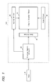
- FIG. 1 is a block diagram for describing a configuration of a liquid crystal display device 100 according to a first embodiment of the present invention.
- the liquid crystal display device 100 includes a liquid crystal panel 10, a display control circuit 20, a source driver 30, a gate driver 40, and a Vcom driver 50.
- the display control circuit 20 represents the display controller.
- the source driver 30 represents the data line drive circuit.
- the gate driver 40 represents the scanning line drive circuit.
- the Vcom driver 50 represents the common electrode drive circuit.
- the source driver 30, the gate driver 40 and the Vcom driver 50 constitute the driving section.
- One or both of the source driver 30 and the gate driver 40 may be formed integrally with the liquid crystal panel 10.
- a host 110 which is constituted primarily by a central Processing unit (CPU).
- CPU central Processing unit
- the liquid crystal panel 10 is formed with a plurality of data lines, a plurality of gate lines, and a plurality of pixel formation portions each corresponding to one of intersections made by the data lines and the gate lines.
- the pixel formation portions are disposed in a matrix pattern. Each pixel formation portion is connected to one of the data lines and one of the gate lines which pass through a corresponding one of the intersections.
- the liquid crystal panel 10 is also formed with a common electrode arranged commonly to the plurality of pixel formation portions. In the present embodiment, the liquid crystal panel 10 is provided by one which employs a normally-black method.
- the display control circuit 20 receives image data and a synchronization signal from the external host 110. In the present DESCRIPTION, it is assumed that the image data represents an image expressed in 8-bit gradation (using 256 gradation levels). Based on the image data and the synchronization signal received, the display control circuit 20 generates and outputs various signals for controlling the source driver 30 and the gate driver 40. The display control circuit 20 also outputs the image data to the source driver 30 at times of counter refreshing and coercive refreshing. The display control circuit 20 may also generate and output various signals for controlling the Vcom driver 50.
- the display control circuit 20 controls the source driver 30 and the gate driver 40 to implement an intermission driving based on AC driving by alternately repeating a drive period for refreshing the screen of liquid crystal panel 10 by writing data voltages based on the image data from the host 110 to the pixel formation portions, and an intermission period for stopping data voltage writing to the pixel formation portions. While the display control circuit 20 provides the drive period at a predetermined timing, it also provides the drive period coercively when the image, which is represented by the image data from the host 110, is updated during the intermission period; in this case, the intermission period is aborted. In other words, the display control circuit 20 performs counter refreshing and coercive refreshing.
- the display control circuit 20 sets the drive period and the intermission period universally across the screen.
- the display control circuit 20 makes the source driver 30 and the gate driver 40 respectively drive the data lines and the scanning lines in the drive period, while making the source driver 30 and the gate driver 40 respectively stop driving of the data lines and scanning lines in the intermission period.
- the source driver 30 generates data voltages based on various signals and the image data from the display control circuit 20, and supplies these data voltages to the data lines, in the drive period.
- the gate driver 40 selects the scanning lines sequentially based on various signals from the display control circuit 20, in the drive period.
- the Vcom driver 50 gives the common electrode a common voltage.
- the data voltage is written to one of the pixel formation portions connected to a selected one of the scanning lines. In this way, a data voltage is written into each pixel formation portion, whereby screen refreshing is performed. In the intermission period, data voltage writing is not performed, so screen refreshing does not take place.
- the source driver 30 performs dot-inversion driving, i.e. a type of the AC driving, based on control by the display control circuit 20.
- the source driver 30 controls data voltage polarity as follows: Specifically, the source driver 30 inverts data voltage polarity for each data line, and also inverts polarity for each scanning line selection period (1 horizontal period) in which one scanning line is selected. In other words, data voltage polarity is inverted for every column and every row.
- the source driver 30 also inverts polarity of data voltage to be written to each pixel formation portion, for every counter refreshing. With details to be described later, at the time of coercive refreshing, the source driver 30 makes polarity of the data voltage to be written for each pixel formation portion identical with the polarity of data voltage which was written to the pixel formation portion in the immediately preceding counter refreshing.
- the source driver 30 performs line-inversion driving of inverting data voltage polarity for each predetermined number of rows, or column-inversion driving of inverting data voltage polarity for each predetermined number of columns.
- the source driver 30 inverts the polarity of data voltage to be written to each pixel formation portion, like in the dot-inversion driving, i.e., for every counter refreshing.
- the source driver 30 may perform frame-inversion driving in which all pixel formation portions are given data voltages of the same polarity, and the polarity of data voltage to be written to pixel formation portion is inverted for every counter refreshing.
- FIG. 2 is an equivalent circuit diagram of a pixel formation portion 11 which is included in the liquid crystal panel shown in FIG. 1 .
- the pixel formation portion 11 includes: a TFT 12 which has its gate terminal as a control terminal connected to a scanning line GL that passes through the corresponding intersection, and has its source terminal as a first conduction terminal connected to a data line SL that passes through said corresponding intersection; a pixel electrode 13 which is connected to a drain terminal, serving as a second conduction terminal, of the TFT 12; a common electrode 14 which is provided commonly to a plurality of the pixel formation portions 11; and a liquid crystal layer which is sandwiched between the pixel electrode 13 and the common electrode 14 and is common to the pixel formation portions 11.
- the pixel electrode 13 and the common electrode 14 form a liquid crystal capacitance Clc, which constitutes a pixel capacitance.
- a liquid crystal capacitance Clc which constitutes a pixel capacitance.
- an auxiliary capacitance in parallel with the liquid crystal capacitance Clc in order to ensure a voltage held in the pixel capacitance; however, for the sake of descriptive convenience, the present DESCRIPTION assumes that the pixel capacitance consists only of the liquid crystal capacitance Clc.
- the liquid crystal capacitance Clc holds a liquid crystal application voltage, which is determined by the data voltage and the common voltage, or more specifically, is given by a difference, right after refreshing, between the data voltage and the common voltage. Note, however, that after the refreshing, liquid crystal dielectric constant changes as the liquid crystal responds to the input, and therefore the liquid crystal application voltage becomes smaller than the difference between the data voltage and the common voltage.
- VA Vertical Alignment
- TN Twisted Nematic
- MVA Multi-domain Vertical Alignment
- IPS In-Plane Switching
- the source driver 30 performs dot-inversion driving in the present embodiment, and therefore the common voltage which the Vcom driver 50 gives to the common electrode 14 has a fixed value. For this reason, the present DESCRIPTION will sometimes treat "holding a data voltage" to be identical with "holding a liquid crystal application voltage".
- the Vcom driver 50 changes the common voltage value according to e.g. refreshing rate, but these will not be covered here.
- the source driver 30 performs line-inversion driving
- the TFT 12 functions as a switching element which assumes an ON state to allow writing of a data voltage to the liquid crystal capacitance Clc, and an OFF state to keep holding the written data voltage (in other words, an electric potential of the pixel electrode 13).
- the TFT 12 may be provided, for example, by an oxide TFT which has its channel layer formed of an oxide semiconductor. Particularly suitable among many oxide TFTs is a TFT whose channel layer is formed of InGaZnOx oxide, i.e., an oxide semiconductor containing indium (In), gallium (Ga), zinc (Zn), and oxygen (O) as primary ingredients (hereinafter called "IGZO-TFT").
- IGZO-TFTs feature a significantly smaller off-leak current than silicon TFTs which use, e.g., amorphous silicon to form the channel layer. Therefore, IGZO-TFTs can hold a data voltage for a long time once it is written to the liquid crystal capacitance Clc.
- oxide semiconductors include at least one of indium, gallium, zinc, copper (Cu), silicon (Si), tin (Sn), aluminum (Al), calcium (Ca), germanium (Ge), and lead (Pb).
- FIG. 3 is a block diagram for describing a configuration of the display control circuit 20 in FIG. 1 .
- the display control circuit 20 includes a frame memory 101, an image information obtaining section 102, an image information storage section 103, a coercive refreshing determination section 104, the refreshing circuit 105, an undershoot circuit 106, a refreshing counter 107, a polarity instruction section 108, and a timing generator 109.
- the frame memory 101 represents the image data storage section.
- the coercive refreshing determination section 104 represents the second refreshing controller.
- the refreshing circuit 105 represents the refreshing section.
- the undershoot circuit 106 represents the gradation correction section.
- the refreshing counter 107 represents the first refreshing controller.
- the frame memory 101 receives one frameful of image data (hereinafter, may also simply called "image data" from the host 110, and stores this one frameful of image data. It should be noted here that frames in the image data are identified, for example, on the basis of a synchronization signal outputted from the host 110; no detailed description therefor will be made here.
- the frame memory 101 receives an active output control signal to be described later from the refreshing circuit 105, whereupon it outputs the stored one frameful of image data to the undershoot circuit 106.
- the image information obtaining section 102 receives one frameful of image data from the host 110, like the frame memory 101.
- the image information obtaining section 102 obtains information of an image (hereinafter called "image information") indicated by the one frameful of image data received, and then outputs the image information to the image information storage section 103 and the coercive refreshing determination section 104.
- image information information of an image
- the image information obtaining section 102 obtains a sum of gradation values of the received one frameful of image, and provides the sum as the image information.
- the image information obtaining section 102 obtains a check sum value of the gradation values in the one frameful of image data, and uses this check sum value as the image information.
- the check sum value has a relatively small data size.
- the image information storage section 103 receives the image information from the image information obtaining section 102, and stores the image information.
- the image information storage section 103 outputs the stored image information to the coercive refreshing determination section 104 in the next frame. Storage of image information received from the image information obtaining section 102 takes place after older image information, which is already in storage, has been outputted to the coercive refreshing determination section 104.
- the coercive refreshing determination section 104 receives current-frame image information and previous-frame image information respectively from the image information obtaining section 102 and the image information storage section 103, and compares the two pieces of image information. If the current-frame image information is different from the previous-frame image information, the coercive refreshing determination section 104 determines that the image represented by the image data has been updated, and then outputs an active coercive refreshing signal to the refreshing circuit 105 and outputs an active correction instruction signal to the undershoot circuit 106. It should be noted here that the coercive refreshing determination section 104 may be designed to determine that the image represented by the image data is not updated if the current-frame image information differs only slightly from the previous-frame image information.
- the coercive refreshing signal represents the second refreshing signal. In the present embodiment, timing for performing a coercive refreshing can be specified by the image information obtaining section 102, the image information storage section 103 and the coercive refreshing determination section 104.
- the refreshing circuit 105 receives the active coercive refreshing signal from the coercive refreshing determination section 104, and an active counter refreshing signal to be described later from the refreshing counter 107, and upon reception of whichever of these, outputs an active output control signal to the frame memory 101. It should be noted here that when an image is updated, then data stored in the frame memory 101 is updated. However, if the image data stored in the frame memory 101 is outputted to the undershoot circuit 106 right after the coercive refreshing determination section 104 determines that the image is updated, then there can be a cases where old image data which represents an image before the update will be outputted to the undershoot circuit 106.
- a certain amount of time e.g., one frame period, is provided between the time when the refreshing circuit 105 receives an active coercive refreshing signal to the time when it outputs the active output control signal to the frame memory 101.
- a certain amount of time e.g., one frame period
- the output of the active coercive refreshing signal from the coercive refreshing determination section 104 is delayed by one frame period.
- the undershoot circuit 106 receives the image data stored in the frame memory 101. If an active correction instruction signal is received from the coercive refreshing determination section 104, then the undershoot circuit 106 makes correction by performing a subtraction operation to the image data received from the frame memory 101, and outputs the corrected image data to the timing generator 109. Specifically, the undershoot circuit 106 decreases gradation values of image data received from the frame memory 101.
- the unit used in changing the gradation value (hereinafter called "gradation unit”) is one gradation.
- decreasing the gradation value by one gradation from a 128-gradation image data will give a 127-gradation image data as a result of the correction
- decreasing the gradation value by two gradations will yield a 126-gradation image data as the corrected data.
- the image data has a smaller gradation value than the gradation value of the image data used in the immediately preceding counter refreshing.
- the data voltage to be written to the liquid crystal capacitance Clc at the time of coercive refreshing has a value closer to the common voltage than does the data voltage written to the liquid crystal capacitance Clc at the time of immediately preceding counter refreshing. If the common voltage is expressed as 0V, a positive-polarity data voltage is expressed as a positive voltage, and a negative-polarity data voltage as a negative voltage, then "the data voltage has a value closer to the common voltage" means that the data voltage has a decreased absolute value.
- a smaller gradation value as a result of the correction performed by the undershoot circuit 106 means that the data voltage to be written to the liquid crystal capacitance Clc at the time of coercive refreshing has a smaller absolute value than the original value. In other words, the data voltage is undershot.
- the undershoot circuit 106 should decrease the gradation value only for the unchanged pixels among the pixels of the updated image; there is no need for decreasing the gradation value for the changed pixels.
- decreasing the gradation value for all of the pixels of an updated image provides an advantage that it is no longer necessary to differentiate the unchanged pixels from the changed pixels, which simplifies the process performed in the undershoot circuit 106.
- the undershoot circuit 106 in the present embodiment decreases the gradation value of the image data from the frame memory 101 for all the pixels if an active correction instruction signal is received from the coercive refreshing determination section 104.
- the present invention is not limited to this, however:
- the undershoot circuit 106 may differentiate unchanged pixels from changed pixels, and decrease gradation values only for the unchanged pixels.
- the undershoot circuit 106 decreases the gradation value of image data received from the frame memory 101 for all pixels, it is not necessary that the amount of change in the gradation value is the same in all of the pixels. Even so, if the undershoot circuit 106 decreases the gradation value of image data received from the frame memory 101 for all pixels, by the same amount of change in the gradation value in all of the pixels, the process to be performed in the undershoot circuit 106 becomes even more simplified.
- the refreshing counter 107 receives the synchronization signal from the host 110, and based on the synchronization signal, increments, for each frame, a count value used for determining the timing to perform counter refreshing. When the count value reaches a predetermined value, the refreshing counter 107 outputs an active counter-refreshing signal to the refreshing circuit 105, and outputs an active polarity-inversion signal for inverting data voltage polarity to the polarity instruction section 108.
- the counter refreshing signal represents the first refreshing signal.
- the refreshing counter 107 resets the count value once the count value reaches the predetermined value.
- the polarity instruction section 108 outputs a polarity signal which indicates data voltage polarity, to the source driver 30.
- the polarity instruction section 108 Upon reception of an active polarity inversion signal from the refreshing counter 107, the polarity instruction section 108 inverts a polarity indicated by the polarity signal. This causes data voltage polarity inversion per counter refreshing. At the time of coercive refreshing, however, the polarity instruction section 108 does not receive an active polarity inversion signal, so data voltage polarity is not inverted.
- the timing generator 109 receives the synchronization signal from the host 110 both in the drive period and in the intermission period, and receives image data from the undershoot circuit 106 in the drive period.
- the image data which the timing generator 109 receives at the time of coercive refreshing is corrected image data corrected by the undershoot circuit 106.
- the undershoot circuit 106 does not receive an active correction instruction signal, so it does not make correction to the image data received from the frame memory 101, and outputs the received image data to the timing generator 109 without making any correction.
- the timing generator 109 generates source control signals such as a source start pulse signal and a source clock signal based on the synchronization signal received and outputs these signals to the source driver 30 while it also generates gate control signals such as a gate start pulse signal and a gate clock signal and output them to the gate driver 40.
- the timing generator 109 adjusts an output timing based on the synchronization signal, and outputs the image data to the source driver 30.
- the timing generator 109 does not receive image data, it makes the source driver 30 and the gate driver 40 stop driving the data lines and scanning lines respectively. For example, the timing generator 109 may stop outputting of the gate control signal and the source control signal when it does not receive image data. This enables to cause the source driver 30 and the gate driver 40 to stop driving the data lines and the scanning lines respectively.
- the timing generator 109 outputs, when it receives image data, an active enable signal to the source driver 30 and the gate driver 40 to allow the source driver 30 and the gate driver 40 to drive the data lines and the scanning lines respectively, whereas the timing generator 109 does not output such an active enable signal when it does not receive image data thereby causing the source driver 30 and the gate driver 40 to stop driving of the data lines and the scanning lines.
- the active enable signal may be outputted by the refreshing counter 107, for example, to the source driver 30 and the gate driver 40, rather than by the timing generator 109.
- FIG. 4 is a diagram for describing an intermission driving according to the present embodiment. Since FIG. 4 is identical with FIG. 15 except for a data voltage at the time of coercive refreshing, description common to both will be appropriately omitted. A focus pixel here is an unchanged pixel.
- data voltages which are applied to the liquid crystal capacitance Clc respectively have positive polarity, negative polarity, positive polarity, and negative polarity. Therefore, in the respective counter refreshings during the first through the fourth intermission driving cycle, liquid crystal application voltages which are applied to the liquid crystal layer respectively have positive polarity, negative polarity, positive polarity, and negative polarity.
- the liquid crystal application voltage changes with time during the intermission period if the image is not updated, and counter refreshing periodically brings the liquid crystal application voltage back to the original value. This keeps the image displayed in the screen.
- a coercive refreshing is performed during the intermission period, in the same fashion as the counter refreshing during the third intermission driving cycle, i.e., a positive-polarity data voltage is used for the writing.
- the undershoot circuit 106 corrects the gradation value of the image data at the time of coercive refreshing and therefore, the data voltage to be written to the liquid crystal capacitance Clc has a value closer to the common voltage than does the data voltage written to the liquid crystal capacitance Clc at the time of counter refreshing in the third intermission driving cycle.
- a liquid crystal application voltage which has a smaller magnitude than the one in the counter refreshing during the third intermission driving cycle is applied to the liquid crystal layer.
- the data voltage to be written to the liquid crystal capacitance Clc at the time of coercive refreshing in the third intermission driving cycle has the same polarity as the data voltage written at the time of counter refreshing in the third intermission driving cycle, but has a value closer to the common voltage than said data voltage, unlike the intermission driving shown in FIG. 15 .
- FIG. 5 shows how the liquid crystal application voltage (absolute value) and brightness change in the intermission driving shown in FIG. 4 .
- a period from the second counter refreshing from the left to the third counter refreshing from the left corresponds to the third intermission driving cycle in FIG. 4 .
- the liquid crystal application voltage increases when a data voltage is written to the liquid crystal capacitance Clc at the time of refreshing, and then decreases as time passes.
- the liquid crystal application voltage increases as a data voltage is written in the counter refreshing; then the liquid crystal application voltage begins decreasing as time passes; but on its way down, a coercive refreshing takes place.
- the present embodiment differs from the example shown in FIG. 15 and FIG. 16 ; i.e., at the time of coercive refreshing, a data voltage which has the same polarity as the data voltage written in the immediately preceding counter refreshing but has a value closer to the common voltage than does that data voltage is written to the liquid crystal capacitance Clc.
- This reduces increase in the liquid crystal application voltage at the time of coercive refreshing, and therefore reduces increase in the effective value of the liquid crystal application voltage. Consequently, as shown in FIG. 5 , it is possible to suppress brightness change which can occur at the time of image update.
- FIG. 5 shows a slight difference between the liquid crystal application voltage at the time of the coercive refreshing and the voltage immediately before that. It is desirable to design the image data gradation value correction so that these two liquid crystal application voltages will be identical with each other by taking into account how the liquid crystal application voltage will change after the counter refreshing. In other words, it is desirable that the amount of correction to be made to the gradation value in the undershoot circuit 106 should be the amount which makes the liquid crystal application voltage at the time of the coercive refreshing identical with the liquid crystal application voltage immediately before that.
- the undershoot circuit 106 converts 8-bit gradation image data (i.e., image data having 256 gradation levels) into 10-bit gradation image data (image data having 1024 gradation levels), so that image data correction can be made using a gradation unit which is practically 1/4 of the original size.
- 8-bit gradation image data image data having 2 X gradation levels
- X-bit gradation image data image data having 2 X gradation levels
- 1 gradation in the 10-bit gradation expression is equal to 0.25 gradations in the 8-bit gradation expression, and therefore conversion from 8-bit gradation image data to 10-bit gradation image data makes the gradation unit 1/4 in effect. For example, if 512 gradations in the 10-bit gradation expression is decreased by 6 gradations, to 506 gradations, the result in effect is 126.5 gradations in the 8-bit gradation expression.
- intermission driving based on AC driving is performed and the drive period and the intermission period are provided universally across the screen in the liquid crystal display device 100.
- a pixel formation portion provides an unchanged pixel at the time of coercive refreshing
- a data voltage which is written to the liquid crystal capacitance Clc has the same polarity as of the data voltage written in the immediately preceding counter refreshing, and a value which is closer to the common voltage than does that data voltage.
- This reduces increase in the liquid crystal application voltage at the time of coercive refreshing, and therefore reduces increase in the effective value of the liquid crystal application voltage. Therefore it is possible to suppress potential brightness change at the time of image update.
- a check sum value of gradation values of one frameful of image data is stored in the image information storage section 103 as image information. Since the check sum value has a relatively small data size, the arrangement allows the image information storage section 103 to be of a relatively small memory size.
- the TFT 12 is provided by an IGZO-TFT. Since IGZO-TFTs feature a significantly small off-leak current, the liquid crystal application voltage does not change significantly. This makes it possible to extend the intermission period for decreased power consumption.
- the image information obtaining section 102 obtains a gradation value histogram (hereinafter called "gradation histogram") of one frameful of image data received by the host 110, and uses this as the image information.
- FIG. 6 shows an example of the gradation histogram according to the present variation.
- the vertical axis and the horizontal axis represent frequency (number of times) and gradation respectively.
- the image information obtaining section 102 obtains gradation values of one frameful of image data received from the host 110, and uses this as the image information. Specifically, the image information obtaining section 102 uses one frameful of image data received from the host 110, as the image information. Therefore, according to the present variation, the image information storage section 103 has the same configuration as the frame memory 101.
- the first variation of the first embodiment can increase image update identification accuracy by the coercive refreshing determination section 104 over the first embodiment, two color images will be determined as the same if, for example, all pixels have the same gradation, even if the two images have different colors. Also, for example, an image in which pixels in the left half of the image have a white gradation and pixels in the right half of the image have a black gradation is misjudged as the same as an image in which pixels in the left half of the image have a black gradation and pixels in the right half of the image have a white gradation.
- the image information is provided by one frameful of image data, so it is possible to compare color data for each pixel.
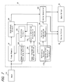
- FIG. 7 is a block diagram for describing a configuration of a display control circuit 20 according to a third variation of the first embodiment.
- image data and a synchronization signal are outputted from the host 110 only at the time of image update. Due to this arrangement, the refreshing counter 107 in the present variation cannot increment the count value based on the synchronization signal, so it has an internal clock generation circuit 107a to generate an internal clock signal.
- the internal clock signal functions as an equivalent of the synchronization signal in the first embodiment.
- the refreshing counter 107 operates in the same way as it operates in the first embodiment based on synchronization signal.
- the timing generator 109 in the present variation cannot operate as it does in the first embodiment based on the synchronization signal, so it receives the internal clock signal from the internal clock generation circuit 107a, and operates in the same way as in the first embodiment.
- the synchronization signal which is outputted from the host 110 only at the time of image update is utilized, as described earlier, to identify frames in the image data. This synchronization signal may be given to the refreshing counter 107 or to the timing generator 109.
- the host 110 outputs image data and a synchronization signal only at the time of image update, and writing of the image data to the frame memory 101 takes place. Therefore, it is possible to decrease power consumption.
- FIG. 8 is a block diagram for describing a configuration of a display control circuit 20 according to a fourth variation of the first embodiment.
- the display control circuit 20 in the present variation is the one according to the third variation of the first embodiment which does not include, however, the image information obtaining section 102, the image information storage section 103, and the coercive refreshing determination section 104. Since the host 110 outputs image data and a synchronization signal only at the time of image update as described above, it is possible to specify the coercive refreshing timing without the image information obtaining section 102, the image information storage section 103 and the coercive refreshing determination section 104. In this way, according to the present variation, it is possible to reduce the circuit size of the display control circuit 20 by eliminating the image information obtaining section 102, the image information storage section 103 and the coercive refreshing determination section 104.
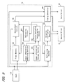
- FIG. 9 is a block diagram for describing a configuration of a display control circuit 20 according to a fifth variation of the first embodiment.
- the display control circuit 20 in the present variation gives image data which is outputted from the host 110 according to the first embodiment, not only to the frame memory 101 and the image information obtaining section 102 but also to the undershoot circuit 106.
- the coercive refreshing determination section 104 outputs an active correction instruction signal but does not output an active coercive refreshing signal upon determination that image data indicates that the image represented thereby is updated. Because of this arrangement, in the present variation, image data stored in the frame memory 101 is not outputted to the undershoot circuit 106 at the time of coercive refreshing.
- the undershoot circuit 106 receives imaged data from the host 110 and therefore, at the time of coercive refreshing, it corrects gradation values of the image data received from the host 10, and outputs the corrected image data to the timing generator 109. It should be noted here that the undershoot circuit 106 does not correct image data from the host 110 and output the corrected data, nor does it output image data as received from the host 110, unless it receives an active correction signal.
- the undershoot circuit 106 receives image data which is stored in the frame memory 101 at the time of coercive refreshing. Therefore, as described earlier, it is necessary that a certain amount of time, e.g., one frame period, is provided between the time when the refreshing circuit 105 receives an active coercive refreshing signal to the time when it outputs the active output control signal to the frame memory 101, or that the output of the active coercive refreshing signal from the coercive refreshing determination section 104 is delayed by about one frame period.
- the undershoot circuit 106 receives image data which is outputted from the host 110, at the time of coercive refreshing. Therefore, it is possible to perform data voltage writing based on the corrected image data corrected by the undershoot circuit 106, immediately at the time of an image update.
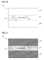
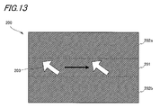
- FIG. 10 is a diagram for describing the partial intermission driving.
- the vertical direction is the column direction and the horizontal direction is the row direction.
- a screen 200 is divided into an updated region 201, and two non-updated regions 202a, 202b sandwiching the updated region 201 in the column direction. As shown in FIG.
- the updated region 201 and the non-updated regions 202a, 202b are identified for each row.
- the update of the image causes a pointer symbol 203 to move from left to right in FIG. 10 .
- the updated region 201 includes both changed pixels and unchanged pixels, and at the time of coercive refreshing, compares with the entire screen according to the first embodiment.
- the updated region 201 is a region constituted by scanning lines GL each connected to pixel formation portions 11 which form the updated region 201 and is a region where these scanning lines GL are taken collectively for sequential selection, at the time of coercive refreshing.
- the present embodiment also assume, like the first embodiment, that it uses a liquid crystal panel 10 of a normally-black method.
- FIG. 11 is a drawing for describing the case where the conventional intermission driving shown in FIG. 15 and FIG. 16 is applied to the partial intermission driving shown in FIG. 10 .
- Image data indicates an image where all the pixels have the same gradation value, except for those pixels that constitute the pointer symbol 203.
- each unchanged pixel in the updated region 201 i.e., the liquid crystal capacitance Clc of the pixel formation portion 11, is given the same data voltage of the same polarity and the same magnitude as of the immediately preceding counter refreshing.
- the liquid crystal application voltage increases again, and the effective value of the liquid crystal application voltage increases.
- this causes brightness change in the unchanged pixels, causing the unchanged pixels in the updated region 201 to be displayed more brightly than those in the non-updated regions 202a, 202b. Therefore, in the second embodiment of the present invention, the intermission driving according to the first embodiment is applied to the partial intermission driving shown in FIG. 10 .
- the two non-updated regions 202a, 202b may be indicated simply by a number 202 when they are not differentiated from each other.
- FIG. 12 is a block diagram for describing a configuration of a display control circuit 20 according to the second embodiment of the present invention. Constituent elements of the present embodiment which are identical with those in the first embodiment will be indicated with the same reference symbols, without repeating description thereof when appropriate.
- the display control circuit 20 in the present embodiment has basically the same configuration as in the first embodiment, but the image information storage section 103 is capable of storing image information for each line. Specifically, as shown in FIG. 12 , the image information storage section 103 has per-line image information storage sub-sections 103a for storage of one-line amount of image information, as many as the number of scanning lines GL.
- the present embodiment performs counter refreshing identically as the first embodiment, so description hereafter will only cover an operation in coercive refreshing.
- the coercive refreshing determination section 104 makes line-by-line comparison between current-frame image information received from the image information obtaining section 102 and previous-frame image information received from the image information storage section 103, and determines that a line is included in the updated region 201 if the comparison reveals difference in image information. At this point, the coercive refreshing determination section 104 outputs an active coercive refreshing signal to the refreshing circuit 105 and outputs an active correction instruction signal to the undershoot circuit 106 like the first embodiment. In this way, determination is made as to whether or not part of the image is updated. The coercive refreshing determination section 104 determines that the line is included in the non-updated region 202 if the current frame and the previous frame have the same image information.
- the coercive refreshing determination section 104 outputs a region signal, for example, for each line to indicates which of the updated region 201 and the non-updated region 202 the line belongs to, to the timing generator 109. Further, it is desirable that the coercive refreshing determination section 104 outputs the region signal also to the refreshing circuit 105 or to the undershoot circuit 106.
- the refreshing circuit 105 Upon reception of the active coercive refreshing signal from the coercive refreshing determination section 104, the refreshing circuit 105 outputs an active output control signal to the frame memory 101. Also, in cases when the coercive refreshing determination section 104 outputs the region signal to the refreshing circuit 105, the refreshing circuit 105 outputs a region indication signal for causing the frame memory 101 to output part of the image data that represents the updated region 201 (hereinafter called "updated-region data”), to the frame memory 101 together with the active output control signal.
- updated-region data a region indication signal for causing the frame memory 101 to output part of the image data that represents the updated region 201
- the frame memory 101 If only the active coercive refreshing signal comes from the refreshing circuit 105, the frame memory 101 outputs one frameful of image data from its storage to the undershoot circuit 106. If the active coercive refreshing signal and the region indication signal come from the refreshing circuit 105, the frame memory 101 outputs updated-region data out of one frameful of image data from its storage, to the undershoot circuit 106.
- the undershoot circuit 106 receives only the updated-region data from the frame memory 101 in the case when it receives only the active correction instruction signal from the coercive refreshing determination section 104. In this way it is possible to make gradation value correction only to the updated-region data.
- the undershoot circuit 106 may receive one frameful of image data or only the updated-region data from the frame memory 101. In this way it is possible to make gradation value correction only to the updated-region data.
- the undershoot circuit 106 outputs corrected updated-region data to the timing generator 109.
- the undershoot circuit 106 may make gradation value correction to the entire frameful of image data, and then output the corrected image data to the timing generator 109. In this case, however, part of the corrected image data representing the non-updated region 202 does not contribute to the refreshing.
- the timing generator 109 instructs the gate driver 40 to scan those scanning lines (included in the updated region 201). For example, the timing generator 109 outputs the above-mentioned active enable signal to the gate driver 40 for each line, thereby instructing the gate driver 40 which of the scanning lines to be scanned.
- the gate driver 40 operates its internal shift registers, it operates each buffer amplifier located between the scanning line which must be scanned and the corresponding stage of the shift register whereas it stops the other buffer amplifiers, to implement scanning of the desired scanning lines.
- the method for scanning desired scanning lines is not limited to the one described here, but any conventional methods maybe employed appropriately.
- the timing generator 109 Based on the updated-region data or image data received from the undershoot circuit 106 and also on the synchronization signal received from the host 110, the timing generator 109 operates the same way as it does in the first embodiment based on image data received from the undershoot circuit 106 and the synchronization signal received from the host 110, so description thereof will not be repeated here. As described above, it is possible to perform coercive refreshing only in the updated region 201 while continuing intermission period in the non-the updated region 201.
- FIG. 13 is a diagram for describing the partial intermission driving according to the present embodiment.
- the updated region 201 undergoes the same driving as in the first embodiment at the time of coercive refreshing.
- data voltages to be written to the liquid crystal capacitances Clc in the pixel formation portions 11 of the unchanged pixels within the updated region 201 are closer to the common voltage than data voltages written to the liquid crystal capacitance Clc in the immediately preceding counter refreshing.
- smaller liquid crystal application voltages than those used at the time of the immediately preceding counter refreshing are applied to the liquid crystal layer at the time of coercive refreshing.
- the arrangement reduces increase in the liquid crystal application voltage at the time of coercive refreshing, and therefore reduces increase in the effective value of the liquid crystal application voltage.
- brightness change which can occur in the updated region 201 at the time of image update is suppressed.
- the present embodiment it is possible to reduce power consumption more than in the first embodiment by employing partial intermission driving. Also, since the updated region 201 is driven in the same way as in the first embodiment at the time of coercive refreshing, brightness change which can occur in the updated region 201 at the time of image update is suppressed like in the first embodiment. Thus, it is possible as shown in FIG. 13 , to suppress brightness difference between the updated region 201 and the non-updated region 202.
- the present embodiment is applicable to whichever of the driving like in the first embodiment where drive period and intermission period are set universally across the screen, and the driving like in the second embodiment where partial intermission driving is employed. Note that the present embodiment also assume, like the first and the second embodiments, that it uses a liquid crystal panel 10 of a normally-black method.
- FIG. 14 is a diagram for describing an intermission driving according to the present embodiment.
- An operation at the time of coercive refreshing is the same as in the first embodiment or the second embodiment described already, and therefore will not be repeated here.
- the drive period at the time of counter refreshing consists of a plurality of drive frames, or more specifically, consists of two drive frames.
- the first drive frame is an overshoot drive frame for writing overshot data voltages.
- the overshoot drive frame is followed by a drive frame, or a normal driving frame, for writing normal data voltages which are not overshoot.
- the drive period at the time of counter refreshing may consist of three or more drive frames, with two or more (but less than the total number of drive frames for the counter refreshing) drive frames performed as overshoot drive frames.
- each overshoot drive frame may use different voltage values.
- Gradation value correction for the overshooting can be implemented as follows, using the configuration in the first embodiment ( FIG. 3 ) or in the second embodiment ( FIG. 12 ) :
- the undershoot circuit 106 performs the gradation value correction for the overshooting.
- the undershoot circuit 106 functions as an overshoot circuit at the time of overshoot drive frame, receiving image data outputted from the frame memory 101 based on an active output control signal, correcting the received image data by performing an adding operation, and then outputting the corrected image data to the timing generator 109.
- the undershoot circuit 106 increases the gradation values of image data received from the frame memory 101.
- data voltages based on the corrected image data have values farther from the common voltage than do data voltages based on the image data received from the frame memory 101.
- the common voltage is expressed as 0V
- a positive-polarity data voltage is expressed as a positive voltage
- a negative-polarity data voltage as a negative voltage
- the data voltages based on the corrected image data have greater absolute values than absolute values of data voltages based on the image data which are received from the frame memory 101.
- the data voltage is overshot.
- the undershoot circuit 106 outputs the received image data to the timing generator 109 without making corrections. In this way, driving as shown in FIG. 14 is implemented.
- the undershoot circuit 106 receives a signal which indicates whether the drive frame during the counter refreshing is an overshoot drive frame or the normal driving frame, from the refreshing circuit 105, the refreshing counter 103 or others.
- an overshoot circuit may be provided separately from the undershoot circuit 106, to perform gradation value correction for the overshoot circuit to overshoot.
- the undershoot circuit 106 and the overshoot circuit constitute the gradation correction circuit.
- image data gradation values are corrected in the overshoot drive frame at the time of counter refreshing, and the data voltages are overshot. Therefore, it is possible to suppress brightness change which can occur at the time of polarity-inverting counter refreshing.
- the present invention is not limited to the embodiments described thus far, but may be varied in many ways within the scope of the present invention. For example, description was made only for cases where coercive refreshing is performed only once in an intermission period; however, coercive refreshing may be performed for a plurality of times in an intermission period. In this case, the first coercive refreshing is performed in the same way as described so far.
- data voltage polarity is the same as in the immediately preceding counter refreshing, like in the first coercive refreshing, but data voltage are set to values closer to the common voltage previous data voltages used in the immediately preceding coercive refreshing, or data voltage values which are more or less the same as used in the immediately preceding coercive refreshing are used.
- the liquid crystal panel 10 employs a normally-black method, so gradation value correction performed by the undershoot circuit 106 at the time of coercive refreshing is to decrease the values.
- gradation value correction performed by the undershoot circuit 106 at the time of coercive refreshing is to increase the values.
- the undershoot circuit 106 (or the overshoot circuit) performs correction to decrease the gradation values in the overshoot drive frame.
- the TFT 12 is provided by an oxide TFT such as a IGZO-TFT; however, the present invention is not limited by this.
- the TFT 12 may be provided by such a TFT as an amorphous silicon TFT, a microcrystalline silicon TFT, a continuous grain silicon TFT and a low-temperature polysilicon TFT.
- the second and the third embodiments may be combined with any of the variations according to the first embodiment.
- a display device which comprises a display section including pixel formation portions, and performs an intermission driving of alternately repeating a drive period for refreshing a screen of the display section by writing data voltages which are based on externally received image data to the pixel formation portions; and an intermission period for stopping writing of the data voltages to the pixel formation portions, the display device further comprising a driving section configured to write the data voltages to the pixel formation portions; and a display controller configured to provide the drive period at a predetermined timing, and control the driving section so that, when part of an image represented by the externally received image data is updated during the intermission period, the intermission period is aborted and the drive period is performed coercively in an updated region which includes said updated part, wherein the display controller includes:
- a drive period coercively only to an updated region in the screen (i.e., a region which includes part of the updated image, and more specifically, a region where the scanning lines each connected to corresponding ones of the pixel formation portions are taken collectively for sequential selection) while continuing an ongoing intermission period to the other regions in the screen.
- Pixels included in the updated region but not having their gradation values changed by the image update have their respective pixel formation portions supplied, through writing, with data voltages that have the same polarity as data voltages written in the immediately preceding drive period but have values closer to the common voltage in the coercively provided drive period, than do the data voltages written in the immediately preceding drive period.
- the arrangement reduces increase in application voltage in the coercively provided drive period for the pixels included in the updated region but not having their gradation values changed by the image update; therefore, the arrangement also reduces increase in the effective value of the application voltage in the pixel formation portion. Since brightness change is thus prevented from occurring in the updated region at the time of image update, it is possible to suppress brightness difference between the updated region and the other regions.
- a display device which comprises a display section including pixel formation portions, and performs an intermission driving of alternately repeating a drive period for refreshing a screen of the display section by writing data voltages which are based on externally received image data to the pixel formation portion; and an intermission period for stopping writing of the data voltages to the pixel formation portions, the display device further comprising a driving section configured to write the data voltages to the pixel formation portions; and a display controller configured to provide the drive period at a predetermined timing, and control the driving section so that, when an image represented by the externally received image data is updated during the intermission period, the intermission period is aborted and the drive period is performed coercively, wherein the display controller includes:
- pixel formation portions which form pixels whose gradation values are not changed by the image update are supplied, by writing in a coercively provided drive period, with data voltages that have the same polarity as of data voltages written in the immediately preceding drive period but have values closer to the common voltage than values of the data voltages written in the immediately preceding drive period.
- a thin film transistor which has its channel layer formed of an oxide semiconductor is utilized. Since this thin film transistor features a very small off-leak current, pixel electrode potential change is suppressed. This makes it possible to make the intermission period for decreased power consumption.
- the display device wherein the oxide semiconductor contains indium, gallium, zinc, and oxygen as its principal components.
- the same advantages as offered by Appendix 2 are provided with the use of a thin film transistor which has its channel layer formed of an oxide semiconductor containing indium, gallium, zinc, and oxygen as its primary components.
- a display device which comprises a display section including pixel formation portions, and performs an intermission driving of alternately repeating a drive period for refreshing a screen of the display section by writing data voltages which are based on externally received image data to the pixel formation portions; and an intermission period for stopping writing of the data voltages to the pixel formation portions, the display device further comprising a driving section configured to write the data voltages to the pixel formation portions; and a display controller configured to provide the drive period at a predetermined timing, and control the driving section so that, when an image represented by the externally received image data is updated during the intermission period, the intermission period is aborted and the drive period is performed coercively, wherein the display controller includes:
- pixel formation portions which form pixels whose gradation values are not changed by the image update are supplied, by writing performed in a coercively provided drive period, with data voltages that have the same polarity as of data voltages written in the immediately preceding drive period but have values closer to the common voltage than values of the data voltages written in the immediately preceding drive period.
- gradation values are corrected so that data voltages to be written to the pixel formation portions have values farther from the common voltage than do data voltages based on the image data outputted from the image data storage section in at least the first drive frame of the drive period which is provided at the predetermined timing. This suppresses brightness change which can occur in the drive period which is provided at a predetermined timing.
- a display device which comprises a display section including pixel formation portions, and performs an intermission driving of alternately repeating a drive period for refreshing a screen of the display section by writing data voltages which are based on externally received image data to the pixel formation portions; and an intermission period for stopping writing of the data voltages to the pixel formation portions, the display device further comprising a driving section configured to write the data voltages to the pixel formation portions; and a display controller configured to provide the drive period at a predetermined timing, and control the driving section so that, when part of an image represented by the externally received image data is updated during the intermission period, the intermission period is aborted and the drive period is performed coercively in an updated region which includes said updated part, wherein the display controller includes:
- the display device disclosed in Appendix 5 provides the same advantages as offered by the display device according to Appendix 4, in the arrangement that, at the time of image update, a drive period is provided coercively only for updated regions in the screen, and an intermission period is continued for the other regions in the screen.
- the present invention is applicable to display devices which perform intermission driving, and methods of driving these display devices.
Landscapes
- Engineering & Computer Science (AREA)
- Physics & Mathematics (AREA)
- Computer Hardware Design (AREA)
- General Physics & Mathematics (AREA)
- Theoretical Computer Science (AREA)
- Chemical & Material Sciences (AREA)
- Crystallography & Structural Chemistry (AREA)
- Multimedia (AREA)
- Control Of Indicators Other Than Cathode Ray Tubes (AREA)
- Liquid Crystal Display Device Control (AREA)
- Liquid Crystal (AREA)
Applications Claiming Priority (2)
| Application Number | Priority Date | Filing Date | Title |
|---|---|---|---|
| JP2012211741 | 2012-09-26 | ||
| PCT/JP2013/070392 WO2014050291A1 (fr) | 2012-09-26 | 2013-07-26 | Dispositif d'affichage et procédé de commande de celui-ci |
Publications (2)
| Publication Number | Publication Date |
|---|---|
| EP2902996A1 true EP2902996A1 (fr) | 2015-08-05 |
| EP2902996A4 EP2902996A4 (fr) | 2015-09-16 |
Family
ID=50387705
Family Applications (1)
| Application Number | Title | Priority Date | Filing Date |
|---|---|---|---|
| EP13841236.6A Withdrawn EP2902996A4 (fr) | 2012-09-26 | 2013-07-26 | Dispositif d'affichage et procédé de commande de celui-ci |
Country Status (8)
| Country | Link |
|---|---|
| US (1) | US9390686B2 (fr) |
| EP (1) | EP2902996A4 (fr) |
| JP (1) | JP5889421B2 (fr) |
| KR (1) | KR101657023B1 (fr) |
| CN (1) | CN104641409A (fr) |
| MY (1) | MY168478A (fr) |
| TW (1) | TW201413699A (fr) |
| WO (1) | WO2014050291A1 (fr) |
Families Citing this family (12)
| Publication number | Priority date | Publication date | Assignee | Title |
|---|---|---|---|---|
| US9626920B2 (en) * | 2012-11-20 | 2017-04-18 | Sharp Kabushiki Kaisha | Liquid crystal display device and method for driving same |
| JP6270411B2 (ja) * | 2013-10-25 | 2018-01-31 | シャープ株式会社 | 表示装置、電子機器、および表示装置の制御方法 |
| US9922613B2 (en) * | 2014-07-11 | 2018-03-20 | Sharp Kabushiki Kaisha | Image display device |
| KR20160044144A (ko) * | 2014-10-14 | 2016-04-25 | 삼성디스플레이 주식회사 | 표시장치 및 그것의 구동 방법 |
| WO2017018241A1 (fr) * | 2015-07-24 | 2017-02-02 | シャープ株式会社 | Dispositif d'affichage et son procédé d'excitation |
| KR102445816B1 (ko) * | 2015-08-31 | 2022-09-22 | 삼성디스플레이 주식회사 | 표시 장치 |
| JP6744791B2 (ja) * | 2015-11-11 | 2020-08-19 | 株式会社Joled | 表示装置、表示装置の補正方法、表示装置の製造方法、および表示装置の表示方法 |
| CN105679279B (zh) * | 2016-04-18 | 2018-01-19 | 京东方科技集团股份有限公司 | 自刷新显示驱动装置、驱动方法及显示装置 |
| TWI587280B (zh) * | 2016-10-18 | 2017-06-11 | 友達光電股份有限公司 | 信號控制方法與應用此方法的顯示面板 |
| WO2019053769A1 (fr) * | 2017-09-12 | 2019-03-21 | シャープ株式会社 | Dispositif d'affichage et procédé de commande associé |
| JP7123097B2 (ja) * | 2020-08-20 | 2022-08-22 | シャープ株式会社 | 表示装置 |
| CN113554967A (zh) * | 2021-07-06 | 2021-10-26 | 北京奕斯伟计算技术有限公司 | 像素数据的处理方法、装置、电子设备及存储介质 |
Family Cites Families (20)
| Publication number | Priority date | Publication date | Assignee | Title |
|---|---|---|---|---|
| JP3639588B2 (ja) | 1998-08-18 | 2005-04-20 | 日本碍子株式会社 | ディスプレイの駆動装置及びディスプレイの駆動方法 |
| JP3762568B2 (ja) | 1998-08-18 | 2006-04-05 | 日本碍子株式会社 | ディスプレイの駆動装置及びディスプレイの駆動方法 |
| JP3766926B2 (ja) | 2000-04-28 | 2006-04-19 | シャープ株式会社 | 表示装置の駆動方法およびそれを用いた表示装置ならびに携帯機器 |
| CN1220098C (zh) | 2000-04-28 | 2005-09-21 | 夏普株式会社 | 显示器件、显示器件驱动方法和装有显示器件的电子设备 |
| JP3730159B2 (ja) * | 2001-01-12 | 2005-12-21 | シャープ株式会社 | 表示装置の駆動方法および表示装置 |
| JP2005140959A (ja) * | 2003-11-06 | 2005-06-02 | Rohm Co Ltd | 表示装置及びこれを用いた携帯機器 |
| JP4599049B2 (ja) * | 2003-11-06 | 2010-12-15 | ローム株式会社 | 表示装置及びこれを用いた携帯機器 |
| JP2006184357A (ja) * | 2004-12-27 | 2006-07-13 | Sharp Corp | 外部画像入力装置および外部画像入力処理方法 |
| US8384639B2 (en) * | 2006-02-07 | 2013-02-26 | Sharp Kabushiki Kaisha | Liquid crystal display device and method for emphasizing temporal signal change on a video signal based on at least a polarity for the video signal |
| KR101388588B1 (ko) | 2007-03-14 | 2014-04-23 | 삼성디스플레이 주식회사 | 액정표시장치 |
| KR101222987B1 (ko) * | 2007-05-11 | 2013-01-17 | 엘지디스플레이 주식회사 | 액정표시장치와 그 구동방법 |
| TW200949822A (en) * | 2007-11-26 | 2009-12-01 | Tpo Displays Corp | Display system and method for reducing power consumption of same |
| CN107886916B (zh) * | 2009-12-18 | 2021-09-21 | 株式会社半导体能源研究所 | 液晶显示装置及其驱动方法 |
| JP5734951B2 (ja) * | 2010-03-03 | 2015-06-17 | シャープ株式会社 | 表示装置およびその駆動方法、ならびに液晶表示装置 |
| JP5394305B2 (ja) * | 2010-04-14 | 2014-01-22 | 株式会社メガチップス | 画像処理装置 |
| JP5002041B2 (ja) * | 2010-07-12 | 2012-08-15 | シャープ株式会社 | 液晶表示装置 |
| US9478186B2 (en) * | 2010-10-28 | 2016-10-25 | Sharp Kabushiki Kaisha | Display device with idle periods for data signals |
| JP5236131B1 (ja) * | 2011-09-06 | 2013-07-17 | シャープ株式会社 | 表示装置およびその駆動方法 |
| US9378694B2 (en) * | 2012-01-30 | 2016-06-28 | Sharp Kabushiki Kaisha | Drive control device, display device including the same, and drive control method |
| US20150228239A1 (en) * | 2012-02-07 | 2015-08-13 | Sharp Kabushiki Kaisha | Display device and method of driving the same |
-
2013
- 2013-07-26 WO PCT/JP2013/070392 patent/WO2014050291A1/fr not_active Ceased
- 2013-07-26 KR KR1020157009478A patent/KR101657023B1/ko not_active Expired - Fee Related
- 2013-07-26 CN CN201380048033.7A patent/CN104641409A/zh active Pending
- 2013-07-26 MY MYPI2015000714A patent/MY168478A/en unknown
- 2013-07-26 US US14/428,010 patent/US9390686B2/en not_active Expired - Fee Related
- 2013-07-26 JP JP2014538248A patent/JP5889421B2/ja not_active Expired - Fee Related
- 2013-07-26 EP EP13841236.6A patent/EP2902996A4/fr not_active Withdrawn
- 2013-09-26 TW TW102134866A patent/TW201413699A/zh unknown
Also Published As
| Publication number | Publication date |
|---|---|
| KR20150055034A (ko) | 2015-05-20 |
| MY168478A (en) | 2018-11-09 |
| EP2902996A4 (fr) | 2015-09-16 |
| JP5889421B2 (ja) | 2016-03-22 |
| CN104641409A (zh) | 2015-05-20 |
| US9390686B2 (en) | 2016-07-12 |
| KR101657023B1 (ko) | 2016-09-12 |
| US20150255040A1 (en) | 2015-09-10 |
| WO2014050291A1 (fr) | 2014-04-03 |
| JPWO2014050291A1 (ja) | 2016-08-22 |
| TW201413699A (zh) | 2014-04-01 |
Similar Documents
| Publication | Publication Date | Title |
|---|---|---|
| US9390686B2 (en) | Display device and method for driving the same | |
| US9449571B2 (en) | Display device driving method, display device, and liquid crystal display device | |
| KR101245944B1 (ko) | 액정패널, 이를 구비한 액정표시장치 및 그 구동 방법 | |
| US10497329B2 (en) | Device for changing driving frequency | |
| US8232946B2 (en) | Liquid crystal display and driving method thereof | |
| JP4271414B2 (ja) | 画像表示装置および表示駆動方法 | |
| US9928796B2 (en) | Display device and display method | |
| EP2905772A1 (fr) | Dispositif d'affichage à cristaux liquides et son procédé de pilotage | |
| US9653013B2 (en) | Liquid crystal display device, data line drive circuit, and drive method for liquid crystal display device | |
| US9123306B2 (en) | Gamma voltage generating device, LCD device, and method of driving the LCD device | |
| US20160196789A1 (en) | Liquid crystal display device and driving method therefor | |
| US9530384B2 (en) | Display device that compensates for changes in driving frequency and drive method thereof | |
| US10909938B2 (en) | Display device and method of driving the same | |
| KR20100069900A (ko) | 액정표시장치의 구동장치 및 그 구동방법 | |
| US9349338B2 (en) | Display device and method for driving same | |
| EP2479746A1 (fr) | Dispositif d'affichage à cristaux liquides et son procédé de commande | |
| KR101451740B1 (ko) | 액정표시장치의 구동 장치 | |
| KR101386569B1 (ko) | 액정표시장치의 응답속도 개선 장치 및 방법 | |
| US8564521B2 (en) | Data processing device, method of driving the same and display device having the same | |
| KR20110070549A (ko) | 액정표시장치 | |
| JP2016170443A (ja) | 液晶表示装置、データ線駆動回路、および液晶表示装置の駆動方法 | |
| KR20050055159A (ko) | 액정표시장치 및 그 구동방법 | |
| JP2007316380A (ja) | 電気光学装置、電気光学装置の駆動方法および電子機器 | |
| JP2015197579A (ja) | 電気光学装置、電子機器、及び電子光学装置の駆動方法 | |
| KR20060003610A (ko) | 액정 표시 장치 및 영상 신호 보정 방법 |
Legal Events
| Date | Code | Title | Description |
|---|---|---|---|
| PUAI | Public reference made under article 153(3) epc to a published international application that has entered the european phase |
Free format text: ORIGINAL CODE: 0009012 |
|
| 17P | Request for examination filed |
Effective date: 20150327 |
|
| AK | Designated contracting states |
Kind code of ref document: A1 Designated state(s): AL AT BE BG CH CY CZ DE DK EE ES FI FR GB GR HR HU IE IS IT LI LT LU LV MC MK MT NL NO PL PT RO RS SE SI SK SM TR |
|
| AX | Request for extension of the european patent |
Extension state: BA ME |
|
| RA4 | Supplementary search report drawn up and despatched (corrected) |
Effective date: 20150818 |
|
| RIC1 | Information provided on ipc code assigned before grant |
Ipc: G09G 3/20 20060101ALN20150812BHEP Ipc: G09G 3/36 20060101AFI20150812BHEP |
|
| DAX | Request for extension of the european patent (deleted) | ||
| 17Q | First examination report despatched |
Effective date: 20160704 |
|
| STAA | Information on the status of an ep patent application or granted ep patent |
Free format text: STATUS: THE APPLICATION IS DEEMED TO BE WITHDRAWN |
|
| 18D | Application deemed to be withdrawn |
Effective date: 20161115 |