EP2904648B1 - Couches de passivation pour dispositifs électroniques organiques - Google Patents
Couches de passivation pour dispositifs électroniques organiques Download PDFInfo
- Publication number
- EP2904648B1 EP2904648B1 EP13755966.2A EP13755966A EP2904648B1 EP 2904648 B1 EP2904648 B1 EP 2904648B1 EP 13755966 A EP13755966 A EP 13755966A EP 2904648 B1 EP2904648 B1 EP 2904648B1
- Authority
- EP
- European Patent Office
- Prior art keywords
- layer
- organic
- electronic device
- organic electronic
- polymer
- Prior art date
- Legal status (The legal status is an assumption and is not a legal conclusion. Google has not performed a legal analysis and makes no representation as to the accuracy of the status listed.)
- Not-in-force
Links
- 238000002161 passivation Methods 0.000 title claims description 76
- 229920000642 polymer Polymers 0.000 claims description 126
- 239000000463 material Substances 0.000 claims description 39
- 239000000203 mixture Substances 0.000 claims description 39
- 125000003118 aryl group Chemical group 0.000 claims description 28
- 239000000178 monomer Substances 0.000 claims description 26
- 239000002904 solvent Substances 0.000 claims description 26
- 238000004132 cross linking Methods 0.000 claims description 25
- 238000000151 deposition Methods 0.000 claims description 18
- 229920002313 fluoropolymer Polymers 0.000 claims description 18
- 239000004811 fluoropolymer Substances 0.000 claims description 14
- 239000004065 semiconductor Substances 0.000 claims description 14
- ZWEHNKRNPOVVGH-UHFFFAOYSA-N 2-Butanone Chemical compound CCC(C)=O ZWEHNKRNPOVVGH-UHFFFAOYSA-N 0.000 claims description 12
- 238000004519 manufacturing process Methods 0.000 claims description 12
- 125000003710 aryl alkyl group Chemical group 0.000 claims description 11
- 238000013086 organic photovoltaic Methods 0.000 claims description 11
- 238000006116 polymerization reaction Methods 0.000 claims description 11
- 239000000758 substrate Substances 0.000 claims description 11
- 239000004593 Epoxy Substances 0.000 claims description 10
- 229940114081 cinnamate Drugs 0.000 claims description 9
- WBYWAXJHAXSJNI-VOTSOKGWSA-M trans-cinnamate Chemical compound [O-]C(=O)\C=C\C1=CC=CC=C1 WBYWAXJHAXSJNI-VOTSOKGWSA-M 0.000 claims description 9
- 125000000391 vinyl group Chemical group [H]C([*])=C([H])[H] 0.000 claims description 9
- 229920002554 vinyl polymer Polymers 0.000 claims description 9
- YBYIRNPNPLQARY-UHFFFAOYSA-N 1H-indene Natural products C1=CC=C2CC=CC2=C1 YBYIRNPNPLQARY-UHFFFAOYSA-N 0.000 claims description 8
- 230000005669 field effect Effects 0.000 claims description 8
- CATSNJVOTSVZJV-UHFFFAOYSA-N heptan-2-one Chemical compound CCCCCC(C)=O CATSNJVOTSVZJV-UHFFFAOYSA-N 0.000 claims description 8
- 125000003454 indenyl group Chemical group C1(C=CC2=CC=CC=C12)* 0.000 claims description 8
- 125000002496 methyl group Chemical group [H]C([H])([H])* 0.000 claims description 8
- PEEHTFAAVSWFBL-UHFFFAOYSA-N Maleimide Chemical compound O=C1NC(=O)C=C1 PEEHTFAAVSWFBL-UHFFFAOYSA-N 0.000 claims description 7
- 238000006243 chemical reaction Methods 0.000 claims description 7
- 239000003989 dielectric material Substances 0.000 claims description 7
- 125000000524 functional group Chemical group 0.000 claims description 7
- 239000003960 organic solvent Substances 0.000 claims description 7
- LLHKCFNBLRBOGN-UHFFFAOYSA-N propylene glycol methyl ether acetate Chemical group COCC(C)OC(C)=O LLHKCFNBLRBOGN-UHFFFAOYSA-N 0.000 claims description 7
- XEKOWRVHYACXOJ-UHFFFAOYSA-N Ethyl acetate Chemical compound CCOC(C)=O XEKOWRVHYACXOJ-UHFFFAOYSA-N 0.000 claims description 6
- 125000005842 heteroatom Chemical group 0.000 claims description 6
- 125000000538 pentafluorophenyl group Chemical group FC1=C(F)C(F)=C(*)C(F)=C1F 0.000 claims description 6
- 125000001997 phenyl group Chemical group [H]C1=C([H])C([H])=C(*)C([H])=C1[H] 0.000 claims description 6
- 125000000332 coumarinyl group Chemical group O1C(=O)C(=CC2=CC=CC=C12)* 0.000 claims description 5
- 125000003518 norbornenyl group Chemical group C12(C=CC(CC1)C2)* 0.000 claims description 5
- 239000010409 thin film Substances 0.000 claims description 5
- OAYXUHPQHDHDDZ-UHFFFAOYSA-N 2-(2-butoxyethoxy)ethanol Chemical compound CCCCOCCOCCO OAYXUHPQHDHDDZ-UHFFFAOYSA-N 0.000 claims description 4
- BGTOWKSIORTVQH-UHFFFAOYSA-N cyclopentanone Chemical compound O=C1CCCC1 BGTOWKSIORTVQH-UHFFFAOYSA-N 0.000 claims description 4
- 125000001495 ethyl group Chemical group [H]C([H])([H])C([H])([H])* 0.000 claims description 4
- 239000012212 insulator Substances 0.000 claims description 4
- 239000003381 stabilizer Substances 0.000 claims description 4
- 239000002318 adhesion promoter Substances 0.000 claims description 3
- 125000000956 methoxy group Chemical group [H]C([H])([H])O* 0.000 claims description 3
- 125000000843 phenylene group Chemical group C1(=C(C=CC=C1)*)* 0.000 claims description 3
- 125000004400 (C1-C12) alkyl group Chemical group 0.000 claims description 2
- PDFYOLXVKFUEPM-UHFFFAOYSA-N 1,1,2,2,3,3,4,4,4a,4b,5,5,6,6,7,7,8,8,8a,9,9,9a-docosafluorofluorene Chemical compound FC1(F)C(F)(F)C(F)(F)C(F)(F)C2(F)C1(F)C(F)(F)C1(F)C(F)(F)C(F)(F)C(F)(F)C(F)(F)C12F PDFYOLXVKFUEPM-UHFFFAOYSA-N 0.000 claims description 2
- 125000001140 1,4-phenylene group Chemical group [H]C1=C([H])C([*:2])=C([H])C([H])=C1[*:1] 0.000 claims description 2
- 238000000018 DNA microarray Methods 0.000 claims description 2
- CTQNGGLPUBDAKN-UHFFFAOYSA-N O-Xylene Chemical compound CC1=CC=CC=C1C CTQNGGLPUBDAKN-UHFFFAOYSA-N 0.000 claims description 2
- 239000003431 cross linking reagent Substances 0.000 claims description 2
- 238000000059 patterning Methods 0.000 claims description 2
- 229950011087 perflunafene Drugs 0.000 claims description 2
- UWEYRJFJVCLAGH-IJWZVTFUSA-N perfluorodecalin Chemical compound FC1(F)C(F)(F)C(F)(F)C(F)(F)[C@@]2(F)C(F)(F)C(F)(F)C(F)(F)C(F)(F)[C@@]21F UWEYRJFJVCLAGH-IJWZVTFUSA-N 0.000 claims description 2
- QKENRHXGDUPTEM-UHFFFAOYSA-N perfluorophenanthrene Chemical group FC1(F)C(F)(F)C(F)(F)C(F)(F)C2(F)C3(F)C(F)(F)C(F)(F)C(F)(F)C(F)(F)C3(F)C(F)(F)C(F)(F)C21F QKENRHXGDUPTEM-UHFFFAOYSA-N 0.000 claims description 2
- 239000008096 xylene Substances 0.000 claims description 2
- 125000000325 methylidene group Chemical group [H]C([H])=* 0.000 claims 6
- 239000010410 layer Substances 0.000 description 137
- -1 photoinitiators Substances 0.000 description 63
- 238000000034 method Methods 0.000 description 35
- 239000011230 binding agent Substances 0.000 description 25
- 238000007639 printing Methods 0.000 description 15
- 125000000217 alkyl group Chemical group 0.000 description 13
- 125000001570 methylene group Chemical group [H]C([H])([*:1])[*:2] 0.000 description 12
- 230000008569 process Effects 0.000 description 12
- 230000005855 radiation Effects 0.000 description 12
- 229920001577 copolymer Polymers 0.000 description 11
- JFNLZVQOOSMTJK-KNVOCYPGSA-N norbornene Chemical compound C1[C@@H]2CC[C@H]1C=C2 JFNLZVQOOSMTJK-KNVOCYPGSA-N 0.000 description 10
- 239000000243 solution Substances 0.000 description 10
- YTPLMLYBLZKORZ-UHFFFAOYSA-N Divinylene sulfide Natural products C=1C=CSC=1 YTPLMLYBLZKORZ-UHFFFAOYSA-N 0.000 description 9
- 125000001183 hydrocarbyl group Chemical group 0.000 description 9
- 229910052739 hydrogen Inorganic materials 0.000 description 9
- 238000000576 coating method Methods 0.000 description 8
- 229910052731 fluorine Inorganic materials 0.000 description 8
- 238000004528 spin coating Methods 0.000 description 8
- 239000004971 Cross linker Substances 0.000 description 7
- HSFWRNGVRCDJHI-UHFFFAOYSA-N alpha-acetylene Natural products C#C HSFWRNGVRCDJHI-UHFFFAOYSA-N 0.000 description 7
- 125000002534 ethynyl group Chemical group [H]C#C* 0.000 description 7
- 125000004435 hydrogen atom Chemical group [H]* 0.000 description 7
- 238000012546 transfer Methods 0.000 description 7
- 150000003923 2,5-pyrrolediones Chemical class 0.000 description 6
- 238000005229 chemical vapour deposition Methods 0.000 description 6
- 239000011248 coating agent Substances 0.000 description 6
- ZYGHJZDHTFUPRJ-UHFFFAOYSA-N coumarin Chemical compound C1=CC=C2OC(=O)C=CC2=C1 ZYGHJZDHTFUPRJ-UHFFFAOYSA-N 0.000 description 6
- 239000001257 hydrogen Substances 0.000 description 6
- 229930192474 thiophene Natural products 0.000 description 6
- 125000002023 trifluoromethyl group Chemical group FC(F)(F)* 0.000 description 6
- 0 *OC(C(C1)N2C=CC1C2)=O Chemical compound *OC(C(C1)N2C=CC1C2)=O 0.000 description 5
- 239000000654 additive Substances 0.000 description 5
- 239000000460 chlorine Substances 0.000 description 5
- 150000001875 compounds Chemical class 0.000 description 5
- 229910052736 halogen Inorganic materials 0.000 description 5
- 150000002367 halogens Chemical class 0.000 description 5
- 238000007641 inkjet printing Methods 0.000 description 5
- 239000007788 liquid Substances 0.000 description 5
- 238000005240 physical vapour deposition Methods 0.000 description 5
- UFHFLCQGNIYNRP-UHFFFAOYSA-N Hydrogen Chemical compound [H][H] UFHFLCQGNIYNRP-UHFFFAOYSA-N 0.000 description 4
- PPBRXRYQALVLMV-UHFFFAOYSA-N Styrene Chemical compound C=CC1=CC=CC=C1 PPBRXRYQALVLMV-UHFFFAOYSA-N 0.000 description 4
- 125000005605 benzo group Chemical group 0.000 description 4
- 229910052801 chlorine Inorganic materials 0.000 description 4
- 150000002118 epoxides Chemical class 0.000 description 4
- 239000010408 film Substances 0.000 description 4
- 229910052751 metal Inorganic materials 0.000 description 4
- 239000002184 metal Substances 0.000 description 4
- YCWSUKQGVSGXJO-NTUHNPAUSA-N nifuroxazide Chemical group C1=CC(O)=CC=C1C(=O)N\N=C\C1=CC=C([N+]([O-])=O)O1 YCWSUKQGVSGXJO-NTUHNPAUSA-N 0.000 description 4
- 229910052757 nitrogen Inorganic materials 0.000 description 4
- 229910052760 oxygen Inorganic materials 0.000 description 4
- 238000012545 processing Methods 0.000 description 4
- 229910052709 silver Inorganic materials 0.000 description 4
- 239000000126 substance Substances 0.000 description 4
- 229910052717 sulfur Inorganic materials 0.000 description 4
- OKTJSMMVPCPJKN-UHFFFAOYSA-N Carbon Chemical group [C] OKTJSMMVPCPJKN-UHFFFAOYSA-N 0.000 description 3
- PXGOKWXKJXAPGV-UHFFFAOYSA-N Fluorine Chemical compound FF PXGOKWXKJXAPGV-UHFFFAOYSA-N 0.000 description 3
- KFZMGEQAYNKOFK-UHFFFAOYSA-N Isopropanol Chemical compound CC(C)O KFZMGEQAYNKOFK-UHFFFAOYSA-N 0.000 description 3
- OKKJLVBELUTLKV-UHFFFAOYSA-N Methanol Chemical compound OC OKKJLVBELUTLKV-UHFFFAOYSA-N 0.000 description 3
- 239000004809 Teflon Substances 0.000 description 3
- 229920006362 Teflon® Polymers 0.000 description 3
- 125000002947 alkylene group Chemical group 0.000 description 3
- XYLMUPLGERFSHI-UHFFFAOYSA-N alpha-Methylstyrene Chemical compound CC(=C)C1=CC=CC=C1 XYLMUPLGERFSHI-UHFFFAOYSA-N 0.000 description 3
- 230000015572 biosynthetic process Effects 0.000 description 3
- 229960000956 coumarin Drugs 0.000 description 3
- 235000001671 coumarin Nutrition 0.000 description 3
- 230000008021 deposition Effects 0.000 description 3
- 239000007772 electrode material Substances 0.000 description 3
- 238000001704 evaporation Methods 0.000 description 3
- 230000008020 evaporation Effects 0.000 description 3
- 239000011737 fluorine Substances 0.000 description 3
- 125000001153 fluoro group Chemical group F* 0.000 description 3
- 125000005843 halogen group Chemical group 0.000 description 3
- 125000001072 heteroaryl group Chemical group 0.000 description 3
- 239000002346 layers by function Substances 0.000 description 3
- QSHDDOUJBYECFT-UHFFFAOYSA-N mercury Chemical compound [Hg] QSHDDOUJBYECFT-UHFFFAOYSA-N 0.000 description 3
- 229910052753 mercury Inorganic materials 0.000 description 3
- 150000002848 norbornenes Chemical class 0.000 description 3
- 229920005548 perfluoropolymer Polymers 0.000 description 3
- 229920003050 poly-cycloolefin Polymers 0.000 description 3
- 230000035945 sensitivity Effects 0.000 description 3
- 125000003107 substituted aryl group Chemical group 0.000 description 3
- 238000003786 synthesis reaction Methods 0.000 description 3
- 229910052724 xenon Inorganic materials 0.000 description 3
- FHNFHKCVQCLJFQ-UHFFFAOYSA-N xenon atom Chemical compound [Xe] FHNFHKCVQCLJFQ-UHFFFAOYSA-N 0.000 description 3
- 150000005072 1,3,4-oxadiazoles Chemical class 0.000 description 2
- HHBBIOLEJRWIGU-UHFFFAOYSA-N 4-ethoxy-1,1,1,2,2,3,3,4,5,6,6,6-dodecafluoro-5-(trifluoromethyl)hexane Chemical compound CCOC(F)(C(F)(C(F)(F)F)C(F)(F)F)C(F)(F)C(F)(F)C(F)(F)F HHBBIOLEJRWIGU-UHFFFAOYSA-N 0.000 description 2
- 125000001318 4-trifluoromethylbenzyl group Chemical group [H]C1=C([H])C(=C([H])C([H])=C1C([H])([H])*)C(F)(F)F 0.000 description 2
- UJOBWOGCFQCDNV-UHFFFAOYSA-N 9H-carbazole Chemical compound C1=CC=C2C3=CC=CC=C3NC2=C1 UJOBWOGCFQCDNV-UHFFFAOYSA-N 0.000 description 2
- XKRFYHLGVUSROY-UHFFFAOYSA-N Argon Chemical compound [Ar] XKRFYHLGVUSROY-UHFFFAOYSA-N 0.000 description 2
- KAKZBPTYRLMSJV-UHFFFAOYSA-N Butadiene Chemical compound C=CC=C KAKZBPTYRLMSJV-UHFFFAOYSA-N 0.000 description 2
- PCBPVYHMZBWMAZ-UHFFFAOYSA-N CC(C1)C2C=CC1C2 Chemical compound CC(C1)C2C=CC1C2 PCBPVYHMZBWMAZ-UHFFFAOYSA-N 0.000 description 2
- VLZOUOXVUMOUML-UHFFFAOYSA-N CCCCCC(C1OC1)C(C1)C2C=CC1C2 Chemical compound CCCCCC(C1OC1)C(C1)C2C=CC1C2 VLZOUOXVUMOUML-UHFFFAOYSA-N 0.000 description 2
- 239000004215 Carbon black (E152) Substances 0.000 description 2
- 229920001609 Poly(3,4-ethylenedioxythiophene) Polymers 0.000 description 2
- 239000004642 Polyimide Substances 0.000 description 2
- 239000004793 Polystyrene Substances 0.000 description 2
- BQCADISMDOOEFD-UHFFFAOYSA-N Silver Chemical compound [Ag] BQCADISMDOOEFD-UHFFFAOYSA-N 0.000 description 2
- XBDYBAVJXHJMNQ-UHFFFAOYSA-N Tetrahydroanthracene Natural products C1=CC=C2C=C(CCCC3)C3=CC2=C1 XBDYBAVJXHJMNQ-UHFFFAOYSA-N 0.000 description 2
- 125000003545 alkoxy group Chemical group 0.000 description 2
- MWPLVEDNUUSJAV-UHFFFAOYSA-N anthracene Chemical compound C1=CC=CC2=CC3=CC=CC=C3C=C21 MWPLVEDNUUSJAV-UHFFFAOYSA-N 0.000 description 2
- 239000003963 antioxidant agent Substances 0.000 description 2
- 125000004429 atom Chemical group 0.000 description 2
- 229910052794 bromium Inorganic materials 0.000 description 2
- 229910052799 carbon Inorganic materials 0.000 description 2
- 239000003054 catalyst Substances 0.000 description 2
- YCIMNLLNPGFGHC-UHFFFAOYSA-N catechol Chemical compound OC1=CC=CC=C1O YCIMNLLNPGFGHC-UHFFFAOYSA-N 0.000 description 2
- 239000003795 chemical substances by application Substances 0.000 description 2
- WDECIBYCCFPHNR-UHFFFAOYSA-N chrysene Chemical compound C1=CC=CC2=CC=C3C4=CC=CC=C4C=CC3=C21 WDECIBYCCFPHNR-UHFFFAOYSA-N 0.000 description 2
- 239000002131 composite material Substances 0.000 description 2
- 229910052802 copper Inorganic materials 0.000 description 2
- VPUGDVKSAQVFFS-UHFFFAOYSA-N coronene Chemical compound C1=C(C2=C34)C=CC3=CC=C(C=C3)C4=C4C3=CC=C(C=C3)C4=C2C3=C1 VPUGDVKSAQVFFS-UHFFFAOYSA-N 0.000 description 2
- 125000004093 cyano group Chemical group *C#N 0.000 description 2
- 125000004122 cyclic group Chemical group 0.000 description 2
- 125000000113 cyclohexyl group Chemical group [H]C1([H])C([H])([H])C([H])([H])C([H])(*)C([H])([H])C1([H])[H] 0.000 description 2
- 238000013461 design Methods 0.000 description 2
- ZUOUZKKEUPVFJK-UHFFFAOYSA-N diphenyl Chemical compound C1=CC=CC=C1C1=CC=CC=C1 ZUOUZKKEUPVFJK-UHFFFAOYSA-N 0.000 description 2
- 239000006185 dispersion Substances 0.000 description 2
- 125000003700 epoxy group Chemical group 0.000 description 2
- 150000002148 esters Chemical class 0.000 description 2
- 238000005530 etching Methods 0.000 description 2
- 238000009472 formulation Methods 0.000 description 2
- 239000011521 glass Substances 0.000 description 2
- 229910052737 gold Inorganic materials 0.000 description 2
- 238000007646 gravure printing Methods 0.000 description 2
- 125000000623 heterocyclic group Chemical group 0.000 description 2
- 229920001519 homopolymer Polymers 0.000 description 2
- 229930195733 hydrocarbon Natural products 0.000 description 2
- 150000002430 hydrocarbons Chemical class 0.000 description 2
- 239000003999 initiator Substances 0.000 description 2
- 229910052740 iodine Inorganic materials 0.000 description 2
- 238000001459 lithography Methods 0.000 description 2
- 238000005259 measurement Methods 0.000 description 2
- 150000002739 metals Chemical class 0.000 description 2
- JRZJOMJEPLMPRA-UHFFFAOYSA-N olefin Natural products CCCCCCCC=C JRZJOMJEPLMPRA-UHFFFAOYSA-N 0.000 description 2
- SLIUAWYAILUBJU-UHFFFAOYSA-N pentacene Chemical compound C1=CC=CC2=CC3=CC4=CC5=CC=CC=C5C=C4C=C3C=C21 SLIUAWYAILUBJU-UHFFFAOYSA-N 0.000 description 2
- 150000002989 phenols Chemical class 0.000 description 2
- 229910052698 phosphorus Inorganic materials 0.000 description 2
- 239000003504 photosensitizing agent Substances 0.000 description 2
- 230000000704 physical effect Effects 0.000 description 2
- 229920003023 plastic Polymers 0.000 description 2
- 239000004033 plastic Substances 0.000 description 2
- 229920003207 poly(ethylene-2,6-naphthalate) Polymers 0.000 description 2
- 229920000647 polyepoxide Polymers 0.000 description 2
- 239000011112 polyethylene naphthalate Substances 0.000 description 2
- 229920000139 polyethylene terephthalate Polymers 0.000 description 2
- 239000005020 polyethylene terephthalate Substances 0.000 description 2
- 229920001721 polyimide Polymers 0.000 description 2
- 229920002223 polystyrene Polymers 0.000 description 2
- BBEAQIROQSPTKN-UHFFFAOYSA-N pyrene Chemical compound C1=CC=C2C=CC3=CC=CC4=CC=C1C2=C43 BBEAQIROQSPTKN-UHFFFAOYSA-N 0.000 description 2
- 230000009467 reduction Effects 0.000 description 2
- 238000007152 ring opening metathesis polymerisation reaction Methods 0.000 description 2
- 238000010020 roller printing Methods 0.000 description 2
- 229910052710 silicon Inorganic materials 0.000 description 2
- 239000004332 silver Substances 0.000 description 2
- 238000007764 slot die coating Methods 0.000 description 2
- 238000010129 solution processing Methods 0.000 description 2
- 125000006850 spacer group Chemical group 0.000 description 2
- 238000010561 standard procedure Methods 0.000 description 2
- 125000000547 substituted alkyl group Chemical group 0.000 description 2
- 125000000999 tert-butyl group Chemical group [H]C([H])([H])C(*)(C([H])([H])[H])C([H])([H])[H] 0.000 description 2
- IFLREYGFSNHWGE-UHFFFAOYSA-N tetracene Chemical compound C1=CC=CC2=CC3=CC4=CC=CC=C4C=C3C=C21 IFLREYGFSNHWGE-UHFFFAOYSA-N 0.000 description 2
- 125000004178 (C1-C4) alkyl group Chemical group 0.000 description 1
- 125000004169 (C1-C6) alkyl group Chemical group 0.000 description 1
- QKAGYSDHEJITFV-UHFFFAOYSA-N 1,1,1,2,2,3,4,5,5,5-decafluoro-3-methoxy-4-(trifluoromethyl)pentane Chemical compound FC(F)(F)C(F)(F)C(F)(OC)C(F)(C(F)(F)F)C(F)(F)F QKAGYSDHEJITFV-UHFFFAOYSA-N 0.000 description 1
- OMCUOJTVNIHQTI-UHFFFAOYSA-N 1,4-bis(4-phenylphenyl)benzene Chemical group C1=CC=CC=C1C1=CC=C(C=2C=CC(=CC=2)C=2C=CC(=CC=2)C=2C=CC=CC=2)C=C1 OMCUOJTVNIHQTI-UHFFFAOYSA-N 0.000 description 1
- 125000004972 1-butynyl group Chemical group [H]C([H])([H])C([H])([H])C#C* 0.000 description 1
- DFUYAWQUODQGFF-UHFFFAOYSA-N 1-ethoxy-1,1,2,2,3,3,4,4,4-nonafluorobutane Chemical compound CCOC(F)(F)C(F)(F)C(F)(F)C(F)(F)F DFUYAWQUODQGFF-UHFFFAOYSA-N 0.000 description 1
- ZEMDSNVUUOCIED-UHFFFAOYSA-N 1-phenyl-4-[4-[4-(4-phenylphenyl)phenyl]phenyl]benzene Chemical group C1=CC=CC=C1C1=CC=C(C=2C=CC(=CC=2)C=2C=CC(=CC=2)C=2C=CC(=CC=2)C=2C=CC=CC=2)C=C1 ZEMDSNVUUOCIED-UHFFFAOYSA-N 0.000 description 1
- 125000000530 1-propynyl group Chemical group [H]C([H])([H])C#C* 0.000 description 1
- KAESVJOAVNADME-UHFFFAOYSA-N 1H-pyrrole Natural products C=1C=CNC=1 KAESVJOAVNADME-UHFFFAOYSA-N 0.000 description 1
- PDQRQJVPEFGVRK-UHFFFAOYSA-N 2,1,3-benzothiadiazole Chemical compound C1=CC=CC2=NSN=C21 PDQRQJVPEFGVRK-UHFFFAOYSA-N 0.000 description 1
- ZZUXQZPDUGRMGP-UHFFFAOYSA-N 2,7-dithiophen-2-yl-9h-carbazole Chemical compound C1=CSC(C=2C=C3C(C4=CC=C(C=C4N3)C=3SC=CC=3)=CC=2)=C1 ZZUXQZPDUGRMGP-UHFFFAOYSA-N 0.000 description 1
- RSZMWIIWUGESRQ-UHFFFAOYSA-N 2-(7-thiophen-2-yl-9h-fluoren-2-yl)thiophene Chemical compound C1=C2CC3=CC(C=4SC=CC=4)=CC=C3C2=CC=C1C1=CC=CS1 RSZMWIIWUGESRQ-UHFFFAOYSA-N 0.000 description 1
- 125000000069 2-butynyl group Chemical group [H]C([H])([H])C#CC([H])([H])* 0.000 description 1
- 125000000094 2-phenylethyl group Chemical group [H]C1=C([H])C([H])=C(C([H])=C1[H])C([H])([H])C([H])([H])* 0.000 description 1
- 125000003903 2-propenyl group Chemical group [H]C([*])([H])C([H])=C([H])[H] 0.000 description 1
- 125000001494 2-propynyl group Chemical group [H]C#CC([H])([H])* 0.000 description 1
- DHDHJYNTEFLIHY-UHFFFAOYSA-N 4,7-diphenyl-1,10-phenanthroline Chemical class C1=CC=CC=C1C1=CC=NC2=C1C=CC1=C(C=3C=CC=CC=3)C=CN=C21 DHDHJYNTEFLIHY-UHFFFAOYSA-N 0.000 description 1
- ZCYVEMRRCGMTRW-UHFFFAOYSA-N 7553-56-2 Chemical compound [I] ZCYVEMRRCGMTRW-UHFFFAOYSA-N 0.000 description 1
- 229920003026 Acene Polymers 0.000 description 1
- 125000006374 C2-C10 alkenyl group Chemical group 0.000 description 1
- 125000005865 C2-C10alkynyl group Chemical group 0.000 description 1
- 125000005915 C6-C14 aryl group Chemical group 0.000 description 1
- XMWRBQBLMFGWIX-UHFFFAOYSA-N C60 fullerene Chemical class C12=C3C(C4=C56)=C7C8=C5C5=C9C%10=C6C6=C4C1=C1C4=C6C6=C%10C%10=C9C9=C%11C5=C8C5=C8C7=C3C3=C7C2=C1C1=C2C4=C6C4=C%10C6=C9C9=C%11C5=C5C8=C3C3=C7C1=C1C2=C4C6=C2C9=C5C3=C12 XMWRBQBLMFGWIX-UHFFFAOYSA-N 0.000 description 1
- UFVCPOAYQVSZJB-UHFFFAOYSA-N CC(C(N1CCC(C2)C3C=CC2C3)=O)=C(C)C1=O Chemical compound CC(C(N1CCC(C2)C3C=CC2C3)=O)=C(C)C1=O UFVCPOAYQVSZJB-UHFFFAOYSA-N 0.000 description 1
- ZAMOUSCENKQFHK-UHFFFAOYSA-N Chlorine atom Chemical compound [Cl] ZAMOUSCENKQFHK-UHFFFAOYSA-N 0.000 description 1
- SNRUBQQJIBEYMU-UHFFFAOYSA-N Dodecane Natural products CCCCCCCCCCCC SNRUBQQJIBEYMU-UHFFFAOYSA-N 0.000 description 1
- 229920001780 ECTFE Polymers 0.000 description 1
- LFQSCWFLJHTTHZ-UHFFFAOYSA-N Ethanol Chemical group CCO LFQSCWFLJHTTHZ-UHFFFAOYSA-N 0.000 description 1
- HAUKRXFFBRKSCF-UHFFFAOYSA-N FC(c1ccc(CC(C2)C3C=CC2C3)cc1)(F)F Chemical compound FC(c1ccc(CC(C2)C3C=CC2C3)cc1)(F)F HAUKRXFFBRKSCF-UHFFFAOYSA-N 0.000 description 1
- PAYRUJLWNCNPSJ-UHFFFAOYSA-N N-phenyl amine Natural products NC1=CC=CC=C1 PAYRUJLWNCNPSJ-UHFFFAOYSA-N 0.000 description 1
- CBENFWSGALASAD-UHFFFAOYSA-N Ozone Chemical compound [O-][O+]=O CBENFWSGALASAD-UHFFFAOYSA-N 0.000 description 1
- 229910019142 PO4 Inorganic materials 0.000 description 1
- ABLZXFCXXLZCGV-UHFFFAOYSA-N Phosphorous acid Chemical class OP(O)=O ABLZXFCXXLZCGV-UHFFFAOYSA-N 0.000 description 1
- 230000010748 Photoabsorption Effects 0.000 description 1
- 239000004952 Polyamide Substances 0.000 description 1
- 239000004698 Polyethylene Substances 0.000 description 1
- 229920000265 Polyparaphenylene Polymers 0.000 description 1
- 239000004743 Polypropylene Substances 0.000 description 1
- 238000003848 UV Light-Curing Methods 0.000 description 1
- QYKIQEUNHZKYBP-UHFFFAOYSA-N Vinyl ether Chemical class C=COC=C QYKIQEUNHZKYBP-UHFFFAOYSA-N 0.000 description 1
- OBASDBHRXUCXKQ-UHFFFAOYSA-N [F].[Br] Chemical compound [F].[Br] OBASDBHRXUCXKQ-UHFFFAOYSA-N 0.000 description 1
- 239000002253 acid Substances 0.000 description 1
- 150000001252 acrylic acid derivatives Chemical class 0.000 description 1
- 239000012190 activator Substances 0.000 description 1
- 125000002252 acyl group Chemical group 0.000 description 1
- 230000000996 additive effect Effects 0.000 description 1
- 150000001298 alcohols Chemical class 0.000 description 1
- 125000003342 alkenyl group Chemical group 0.000 description 1
- 229920000180 alkyd Polymers 0.000 description 1
- 150000003973 alkyl amines Chemical group 0.000 description 1
- 125000000304 alkynyl group Chemical group 0.000 description 1
- 229910052782 aluminium Inorganic materials 0.000 description 1
- 150000001408 amides Chemical class 0.000 description 1
- 150000001412 amines Chemical class 0.000 description 1
- 150000001448 anilines Chemical class 0.000 description 1
- 125000002178 anthracenyl group Chemical group C1(=CC=CC2=CC3=CC=CC=C3C=C12)* 0.000 description 1
- 229910052786 argon Inorganic materials 0.000 description 1
- 150000004982 aromatic amines Chemical group 0.000 description 1
- 150000004945 aromatic hydrocarbons Chemical class 0.000 description 1
- 229920003235 aromatic polyamide Polymers 0.000 description 1
- 229910052785 arsenic Inorganic materials 0.000 description 1
- 239000012298 atmosphere Substances 0.000 description 1
- 230000008901 benefit Effects 0.000 description 1
- HFACYLZERDEVSX-UHFFFAOYSA-N benzidine Chemical class C1=CC(N)=CC=C1C1=CC=C(N)C=C1 HFACYLZERDEVSX-UHFFFAOYSA-N 0.000 description 1
- UMIVXZPTRXBADB-UHFFFAOYSA-N benzocyclobutene Chemical class C1=CC=C2CCC2=C1 UMIVXZPTRXBADB-UHFFFAOYSA-N 0.000 description 1
- 125000001797 benzyl group Chemical group [H]C1=C([H])C([H])=C(C([H])=C1[H])C([H])([H])* 0.000 description 1
- 235000010290 biphenyl Nutrition 0.000 description 1
- 239000004305 biphenyl Substances 0.000 description 1
- 229910052796 boron Inorganic materials 0.000 description 1
- MTAZNLWOLGHBHU-UHFFFAOYSA-N butadiene-styrene rubber Chemical compound C=CC=C.C=CC1=CC=CC=C1 MTAZNLWOLGHBHU-UHFFFAOYSA-N 0.000 description 1
- 125000004369 butenyl group Chemical group C(=CCC)* 0.000 description 1
- 125000005569 butenylene group Chemical group 0.000 description 1
- 125000000484 butyl group Chemical group [H]C([*])([H])C([H])([H])C([H])([H])C([H])([H])[H] 0.000 description 1
- 125000004432 carbon atom Chemical group C* 0.000 description 1
- 150000001735 carboxylic acids Chemical class 0.000 description 1
- 238000005266 casting Methods 0.000 description 1
- 239000001913 cellulose Substances 0.000 description 1
- 229920002678 cellulose Polymers 0.000 description 1
- 229920002301 cellulose acetate Polymers 0.000 description 1
- 239000002800 charge carrier Substances 0.000 description 1
- 238000007385 chemical modification Methods 0.000 description 1
- 238000000224 chemical solution deposition Methods 0.000 description 1
- 229910052804 chromium Inorganic materials 0.000 description 1
- 229920000547 conjugated polymer Polymers 0.000 description 1
- 238000001723 curing Methods 0.000 description 1
- 125000000753 cycloalkyl group Chemical group 0.000 description 1
- 125000001511 cyclopentyl group Chemical group [H]C1([H])C([H])([H])C([H])([H])C([H])(*)C1([H])[H] 0.000 description 1
- 230000003247 decreasing effect Effects 0.000 description 1
- 125000002704 decyl group Chemical group [H]C([H])([H])C([H])([H])C([H])([H])C([H])([H])C([H])([H])C([H])([H])C([H])([H])C([H])([H])C([H])([H])C([H])([H])* 0.000 description 1
- 230000001627 detrimental effect Effects 0.000 description 1
- GYZLOYUZLJXAJU-UHFFFAOYSA-N diglycidyl ether Chemical class C1OC1COCC1CO1 GYZLOYUZLJXAJU-UHFFFAOYSA-N 0.000 description 1
- 239000003085 diluting agent Substances 0.000 description 1
- 238000010790 dilution Methods 0.000 description 1
- 239000012895 dilution Substances 0.000 description 1
- 239000004205 dimethyl polysiloxane Substances 0.000 description 1
- 238000003618 dip coating Methods 0.000 description 1
- 239000002612 dispersion medium Substances 0.000 description 1
- 238000007606 doctor blade method Methods 0.000 description 1
- 125000003438 dodecyl group Chemical group [H]C([H])([H])C([H])([H])C([H])([H])C([H])([H])C([H])([H])C([H])([H])C([H])([H])C([H])([H])C([H])([H])C([H])([H])C([H])([H])C([H])([H])* 0.000 description 1
- 238000001035 drying Methods 0.000 description 1
- 230000000694 effects Effects 0.000 description 1
- 238000010894 electron beam technology Methods 0.000 description 1
- 238000005516 engineering process Methods 0.000 description 1
- 230000007613 environmental effect Effects 0.000 description 1
- 125000005678 ethenylene group Chemical group [H]C([*:1])=C([H])[*:2] 0.000 description 1
- 150000002170 ethers Chemical class 0.000 description 1
- 239000011152 fibreglass Substances 0.000 description 1
- 238000007775 flexo coating Methods 0.000 description 1
- GVEPBJHOBDJJJI-UHFFFAOYSA-N fluoranthrene Natural products C1=CC(C2=CC=CC=C22)=C3C2=CC=CC3=C1 GVEPBJHOBDJJJI-UHFFFAOYSA-N 0.000 description 1
- 238000003682 fluorination reaction Methods 0.000 description 1
- 125000004216 fluoromethyl group Chemical group [H]C([H])(F)* 0.000 description 1
- 229910003472 fullerene Inorganic materials 0.000 description 1
- 230000009477 glass transition Effects 0.000 description 1
- 229910002804 graphite Inorganic materials 0.000 description 1
- 239000010439 graphite Substances 0.000 description 1
- 238000007756 gravure coating Methods 0.000 description 1
- 230000026030 halogenation Effects 0.000 description 1
- 238000005658 halogenation reaction Methods 0.000 description 1
- 125000003187 heptyl group Chemical group [H]C([*])([H])C([H])([H])C([H])([H])C([H])([H])C([H])([H])C([H])([H])C([H])([H])[H] 0.000 description 1
- 125000006038 hexenyl group Chemical group 0.000 description 1
- 125000004051 hexyl group Chemical group [H]C([H])([H])C([H])([H])C([H])([H])C([H])([H])C([H])([H])C([H])([H])* 0.000 description 1
- 229920001903 high density polyethylene Polymers 0.000 description 1
- 239000004700 high-density polyethylene Substances 0.000 description 1
- 125000002887 hydroxy group Chemical group [H]O* 0.000 description 1
- 150000002466 imines Chemical class 0.000 description 1
- AMGQUBHHOARCQH-UHFFFAOYSA-N indium;oxotin Chemical compound [In].[Sn]=O AMGQUBHHOARCQH-UHFFFAOYSA-N 0.000 description 1
- 239000011147 inorganic material Substances 0.000 description 1
- 239000011810 insulating material Substances 0.000 description 1
- 239000011630 iodine Substances 0.000 description 1
- 125000000959 isobutyl group Chemical group [H]C([H])([H])C([H])(C([H])([H])[H])C([H])([H])* 0.000 description 1
- 125000001449 isopropyl group Chemical group [H]C([H])([H])C([H])(*)C([H])([H])[H] 0.000 description 1
- 238000001540 jet deposition Methods 0.000 description 1
- 238000007644 letterpress printing Methods 0.000 description 1
- 125000005647 linker group Chemical group 0.000 description 1
- 239000007791 liquid phase Substances 0.000 description 1
- 125000005439 maleimidyl group Chemical group C1(C=CC(N1*)=O)=O 0.000 description 1
- 239000012528 membrane Substances 0.000 description 1
- 229910044991 metal oxide Inorganic materials 0.000 description 1
- 150000004706 metal oxides Chemical class 0.000 description 1
- 238000001465 metallisation Methods 0.000 description 1
- SYSQUGFVNFXIIT-UHFFFAOYSA-N n-[4-(1,3-benzoxazol-2-yl)phenyl]-4-nitrobenzenesulfonamide Chemical class C1=CC([N+](=O)[O-])=CC=C1S(=O)(=O)NC1=CC=C(C=2OC3=CC=CC=C3N=2)C=C1 SYSQUGFVNFXIIT-UHFFFAOYSA-N 0.000 description 1
- 125000001624 naphthyl group Chemical group 0.000 description 1
- 125000001971 neopentyl group Chemical group [H]C([*])([H])C(C([H])([H])[H])(C([H])([H])[H])C([H])([H])[H] 0.000 description 1
- 229910052759 nickel Inorganic materials 0.000 description 1
- 125000000449 nitro group Chemical group [O-][N+](*)=O 0.000 description 1
- 125000001400 nonyl group Chemical group [H]C([*])([H])C([H])([H])C([H])([H])C([H])([H])C([H])([H])C([H])([H])C([H])([H])C([H])([H])C([H])([H])[H] 0.000 description 1
- 125000002347 octyl group Chemical group [H]C([*])([H])C([H])([H])C([H])([H])C([H])([H])C([H])([H])C([H])([H])C([H])([H])C([H])([H])[H] 0.000 description 1
- 239000011368 organic material Substances 0.000 description 1
- 125000002524 organometallic group Chemical group 0.000 description 1
- MPQXHAGKBWFSNV-UHFFFAOYSA-N oxidophosphanium Chemical class [PH3]=O MPQXHAGKBWFSNV-UHFFFAOYSA-N 0.000 description 1
- 125000004430 oxygen atom Chemical group O* 0.000 description 1
- GPRIERYVMZVKTC-UHFFFAOYSA-N p-quaterphenyl Chemical group C1=CC=CC=C1C1=CC=C(C=2C=CC(=CC=2)C=2C=CC=CC=2)C=C1 GPRIERYVMZVKTC-UHFFFAOYSA-N 0.000 description 1
- 238000007649 pad printing Methods 0.000 description 1
- 229910052763 palladium Inorganic materials 0.000 description 1
- 239000002245 particle Substances 0.000 description 1
- 125000001147 pentyl group Chemical group C(CCCC)* 0.000 description 1
- 125000002080 perylenyl group Chemical group C1(=CC=C2C=CC=C3C4=CC=CC5=CC=CC(C1=C23)=C45)* 0.000 description 1
- CSHWQDPOILHKBI-UHFFFAOYSA-N peryrene Natural products C1=CC(C2=CC=CC=3C2=C2C=CC=3)=C3C2=CC=CC3=C1 CSHWQDPOILHKBI-UHFFFAOYSA-N 0.000 description 1
- ISWSIDIOOBJBQZ-UHFFFAOYSA-N phenol group Chemical group C1(=CC=CC=C1)O ISWSIDIOOBJBQZ-UHFFFAOYSA-N 0.000 description 1
- 235000021317 phosphate Nutrition 0.000 description 1
- 150000003003 phosphines Chemical class 0.000 description 1
- 125000005538 phosphinite group Chemical group 0.000 description 1
- AQSJGOWTSHOLKH-UHFFFAOYSA-N phosphite(3-) Chemical class [O-]P([O-])[O-] AQSJGOWTSHOLKH-UHFFFAOYSA-N 0.000 description 1
- XRBCRPZXSCBRTK-UHFFFAOYSA-N phosphonous acid Chemical class OPO XRBCRPZXSCBRTK-UHFFFAOYSA-N 0.000 description 1
- 150000003013 phosphoric acid derivatives Chemical class 0.000 description 1
- 229910052697 platinum Inorganic materials 0.000 description 1
- 229920000435 poly(dimethylsiloxane) Polymers 0.000 description 1
- 229920003229 poly(methyl methacrylate) Polymers 0.000 description 1
- 229920000052 poly(p-xylylene) Polymers 0.000 description 1
- 229920000553 poly(phenylenevinylene) Polymers 0.000 description 1
- 229920002492 poly(sulfone) Polymers 0.000 description 1
- 229920002647 polyamide Polymers 0.000 description 1
- 229920000767 polyaniline Polymers 0.000 description 1
- 229920000323 polyazulene Polymers 0.000 description 1
- 229920002098 polyfluorene Polymers 0.000 description 1
- 229920000414 polyfuran Polymers 0.000 description 1
- 229920001470 polyketone Polymers 0.000 description 1
- 239000002861 polymer material Substances 0.000 description 1
- 239000004926 polymethyl methacrylate Substances 0.000 description 1
- 229920001155 polypropylene Polymers 0.000 description 1
- 229920000128 polypyrrole Polymers 0.000 description 1
- 229920001296 polysiloxane Polymers 0.000 description 1
- 229920001343 polytetrafluoroethylene Polymers 0.000 description 1
- 239000004810 polytetrafluoroethylene Substances 0.000 description 1
- 229920002635 polyurethane Polymers 0.000 description 1
- 239000004814 polyurethane Substances 0.000 description 1
- 239000004800 polyvinyl chloride Substances 0.000 description 1
- 229920000915 polyvinyl chloride Polymers 0.000 description 1
- 239000002243 precursor Substances 0.000 description 1
- 125000004368 propenyl group Chemical group C(=CC)* 0.000 description 1
- 125000006410 propenylene group Chemical group 0.000 description 1
- 125000001436 propyl group Chemical group [H]C([*])([H])C([H])([H])C([H])([H])[H] 0.000 description 1
- 238000000746 purification Methods 0.000 description 1
- 150000003219 pyrazolines Chemical class 0.000 description 1
- 150000003233 pyrroles Chemical class 0.000 description 1
- 150000003254 radicals Chemical class 0.000 description 1
- 239000011541 reaction mixture Substances 0.000 description 1
- 230000009257 reactivity Effects 0.000 description 1
- 238000007650 screen-printing Methods 0.000 description 1
- 125000002914 sec-butyl group Chemical group [H]C([H])([H])C([H])([H])C([H])(*)C([H])([H])[H] 0.000 description 1
- 229910052711 selenium Inorganic materials 0.000 description 1
- 238000004904 shortening Methods 0.000 description 1
- 150000004756 silanes Chemical class 0.000 description 1
- 239000010703 silicon Substances 0.000 description 1
- 229920002379 silicone rubber Polymers 0.000 description 1
- 239000002356 single layer Substances 0.000 description 1
- 230000002269 spontaneous effect Effects 0.000 description 1
- 238000005507 spraying Methods 0.000 description 1
- 238000004544 sputter deposition Methods 0.000 description 1
- 239000010421 standard material Substances 0.000 description 1
- PJANXHGTPQOBST-UHFFFAOYSA-N stilbene Chemical class C=1C=CC=CC=1C=CC1=CC=CC=C1 PJANXHGTPQOBST-UHFFFAOYSA-N 0.000 description 1
- 238000006467 substitution reaction Methods 0.000 description 1
- 125000004434 sulfur atom Chemical group 0.000 description 1
- 229910052714 tellurium Inorganic materials 0.000 description 1
- 238000002207 thermal evaporation Methods 0.000 description 1
- 150000007970 thio esters Chemical class 0.000 description 1
- 125000004001 thioalkyl group Chemical group 0.000 description 1
- 150000003568 thioethers Chemical class 0.000 description 1
- 150000003573 thiols Chemical class 0.000 description 1
- 150000003577 thiophenes Chemical class 0.000 description 1
- 229910052723 transition metal Inorganic materials 0.000 description 1
- 150000003624 transition metals Chemical class 0.000 description 1
- 150000003918 triazines Chemical class 0.000 description 1
- 238000001771 vacuum deposition Methods 0.000 description 1
Images


Classifications
-
- H—ELECTRICITY
- H10—SEMICONDUCTOR DEVICES; ELECTRIC SOLID-STATE DEVICES NOT OTHERWISE PROVIDED FOR
- H10K—ORGANIC ELECTRIC SOLID-STATE DEVICES
- H10K10/00—Organic devices specially adapted for rectifying, amplifying, oscillating or switching; Organic capacitors or resistors having potential barriers
- H10K10/80—Constructional details
- H10K10/88—Passivation; Containers; Encapsulations
-
- H—ELECTRICITY
- H10—SEMICONDUCTOR DEVICES; ELECTRIC SOLID-STATE DEVICES NOT OTHERWISE PROVIDED FOR
- H10K—ORGANIC ELECTRIC SOLID-STATE DEVICES
- H10K85/00—Organic materials used in the body or electrodes of devices covered by this subclass
- H10K85/10—Organic polymers or oligomers
- H10K85/111—Organic polymers or oligomers comprising aromatic, heteroaromatic, or aryl chains, e.g. polyaniline, polyphenylene or polyphenylene vinylene
-
- H—ELECTRICITY
- H10—SEMICONDUCTOR DEVICES; ELECTRIC SOLID-STATE DEVICES NOT OTHERWISE PROVIDED FOR
- H10K—ORGANIC ELECTRIC SOLID-STATE DEVICES
- H10K85/00—Organic materials used in the body or electrodes of devices covered by this subclass
- H10K85/10—Organic polymers or oligomers
- H10K85/141—Organic polymers or oligomers comprising aliphatic or olefinic chains, e.g. poly N-vinylcarbazol, PVC or PTFE
-
- H—ELECTRICITY
- H10—SEMICONDUCTOR DEVICES; ELECTRIC SOLID-STATE DEVICES NOT OTHERWISE PROVIDED FOR
- H10K—ORGANIC ELECTRIC SOLID-STATE DEVICES
- H10K85/00—Organic materials used in the body or electrodes of devices covered by this subclass
- H10K85/10—Organic polymers or oligomers
- H10K85/151—Copolymers
-
- C—CHEMISTRY; METALLURGY
- C08—ORGANIC MACROMOLECULAR COMPOUNDS; THEIR PREPARATION OR CHEMICAL WORKING-UP; COMPOSITIONS BASED THEREON
- C08L—COMPOSITIONS OF MACROMOLECULAR COMPOUNDS
- C08L45/00—Compositions of homopolymers or copolymers of compounds having no unsaturated aliphatic radicals in side chain, and having one or more carbon-to-carbon double bonds in a carbocyclic or in a heterocyclic ring system; Compositions of derivatives of such polymers
-
- C—CHEMISTRY; METALLURGY
- C08—ORGANIC MACROMOLECULAR COMPOUNDS; THEIR PREPARATION OR CHEMICAL WORKING-UP; COMPOSITIONS BASED THEREON
- C08L—COMPOSITIONS OF MACROMOLECULAR COMPOUNDS
- C08L79/00—Compositions of macromolecular compounds obtained by reactions forming in the main chain of the macromolecule a linkage containing nitrogen with or without oxygen or carbon only, not provided for in groups C08L61/00 - C08L77/00
- C08L79/04—Polycondensates having nitrogen-containing heterocyclic rings in the main chain; Polyhydrazides; Polyamide acids or similar polyimide precursors
- C08L79/08—Polyimides; Polyester-imides; Polyamide-imides; Polyamide acids or similar polyimide precursors
- C08L79/085—Unsaturated polyimide precursors
-
- H—ELECTRICITY
- H10—SEMICONDUCTOR DEVICES; ELECTRIC SOLID-STATE DEVICES NOT OTHERWISE PROVIDED FOR
- H10K—ORGANIC ELECTRIC SOLID-STATE DEVICES
- H10K10/00—Organic devices specially adapted for rectifying, amplifying, oscillating or switching; Organic capacitors or resistors having potential barriers
- H10K10/40—Organic transistors
- H10K10/46—Field-effect transistors, e.g. organic thin-film transistors [OTFT]
- H10K10/462—Insulated gate field-effect transistors [IGFETs]
- H10K10/464—Lateral top-gate IGFETs comprising only a single gate
-
- H—ELECTRICITY
- H10—SEMICONDUCTOR DEVICES; ELECTRIC SOLID-STATE DEVICES NOT OTHERWISE PROVIDED FOR
- H10K—ORGANIC ELECTRIC SOLID-STATE DEVICES
- H10K10/00—Organic devices specially adapted for rectifying, amplifying, oscillating or switching; Organic capacitors or resistors having potential barriers
- H10K10/40—Organic transistors
- H10K10/46—Field-effect transistors, e.g. organic thin-film transistors [OTFT]
- H10K10/462—Insulated gate field-effect transistors [IGFETs]
- H10K10/466—Lateral bottom-gate IGFETs comprising only a single gate
-
- H—ELECTRICITY
- H10—SEMICONDUCTOR DEVICES; ELECTRIC SOLID-STATE DEVICES NOT OTHERWISE PROVIDED FOR
- H10K—ORGANIC ELECTRIC SOLID-STATE DEVICES
- H10K2102/00—Constructional details relating to the organic devices covered by this subclass
- H10K2102/301—Details of OLEDs
- H10K2102/351—Thickness
-
- H—ELECTRICITY
- H10—SEMICONDUCTOR DEVICES; ELECTRIC SOLID-STATE DEVICES NOT OTHERWISE PROVIDED FOR
- H10K—ORGANIC ELECTRIC SOLID-STATE DEVICES
- H10K71/00—Manufacture or treatment specially adapted for the organic devices covered by this subclass
- H10K71/20—Changing the shape of the active layer in the devices, e.g. patterning
-
- Y—GENERAL TAGGING OF NEW TECHNOLOGICAL DEVELOPMENTS; GENERAL TAGGING OF CROSS-SECTIONAL TECHNOLOGIES SPANNING OVER SEVERAL SECTIONS OF THE IPC; TECHNICAL SUBJECTS COVERED BY FORMER USPC CROSS-REFERENCE ART COLLECTIONS [XRACs] AND DIGESTS
- Y02—TECHNOLOGIES OR APPLICATIONS FOR MITIGATION OR ADAPTATION AGAINST CLIMATE CHANGE
- Y02E—REDUCTION OF GREENHOUSE GAS [GHG] EMISSIONS, RELATED TO ENERGY GENERATION, TRANSMISSION OR DISTRIBUTION
- Y02E10/00—Energy generation through renewable energy sources
- Y02E10/50—Photovoltaic [PV] energy
- Y02E10/549—Organic PV cells
Definitions
- the invention generally relates to passivation layers for use in organic electronic devices, and more specifically in organic field effect transistors, to processes for preparing such passivation layers, and to organic electronic devices and organic field effect transistors encompassing such passivation layers.
- a conventional bottom gate OFET comprises a gate electrode, a gate insulator layer made of a dielectric material (also referred to as “dielectric” or “gate dielectric”), source and drain electrodes, a semiconducting layer made of an organic semiconductor (OSC) material, and typically a passivation layer on top of the OSC layer to protect it against environmental influence and/or damage from subsequent device manufacturing steps.
- a dielectric material also referred to as "dielectric” or “gate dielectric”
- OSC organic semiconductor
- passivation layers For OFET devices in particular solution processable passivation layers are desired.
- the key requirements for materials used in such passivation layers are orthogonality of the passivation layer solvent with the OSC layer, and adhesion to the underlying layers.
- the passivation materials should be solution based and should be suitable for solution based deposition methods like spin-coating, or wider area printing methods including flexo, gravure and slot-die coating.
- the passivation layer comprises a layer of a fluorinated polymer and a second layer of a polycycloolefinic polymer comprising crosslinkable groups.
- the second layer increases the adhesion to further layers applied on top of the insulator.
- One aim of the present invention is to provide passivation layers and materials used therein which meet these requirements. Another aim is to provide improved methods of manufacturing such passivation layers. Another aim is to provide improved OE devices, in particular OFETs, more specifically bottom gate OFETs, comprising such passivation layers. Further aims are immediately evident to the person skilled in the art from the following description.
- Such a passivation layer stack was found to provide adequate adhesion to the OSC and between the individual passivation layers, to provide a top surface that is resistant to subsequent device manufacturing steps, especially to metal deposition and etching processes, and to be especially suitable for mass production of OFET devices.
- the bottom layer of the passivation layer stack can also be deposited onto a patterned OSC layer which is provided on an organic gate dielectric layer, so that the adhesion of the bottom layer to both the OSC and the underlying organic gate dielectric should be strong.
- the invention relates an organic electronic device comprising an organic semiconductor (OSC) layer and a passivation layer stack provided on the OSC layer, characterized in that the passivation layer stack comprises
- the organic electronic device is for example an Organic Field Effect Transistor (OFET), including Organic Thin Film Transistors (OTFT), an Organic Light Emitting Diode (OLED), an Organic Photovoltaic (OPV) device or an Organic Photodetector (OPD), especially a top gate OFET or bottom gate OFET, preferably a bottom gate OFET.
- OFET Organic Field Effect Transistor
- OTFT Organic Thin Film Transistors
- OLED Organic Light Emitting Diode
- OPD Organic Photovoltaic
- the invention further relates to a product or an assembly comprising an organic electronic device as described above and below.
- product or assembly is preferably an Integrated Circuit (IC), a Radio Frequency Identification (RFID) tag, a security marking or security device containing an RFID tag, a Flat Panel Display (FPD), a backplane of an FPD, a backlight of an FPD, an electrophotographic device, an electrophotographic recording device, an organic memory device, a sensor, a biosensor or a biochip.
- IC Integrated Circuit
- RFID Radio Frequency Identification
- FPD Flat Panel Display
- FPD Flat Panel Display
- backplane of an FPD a backlight of an FPD
- electrophotographic device an electrophotographic recording device
- organic memory device a sensor, a biosensor or a biochip.
- the invention further relates to a process of preparing a passivation layer stack as described hereinafter.
- the invention further relates to a process of preparing an organic electronic device, especially a top gate OFET or bottom gate OFET, comprising a passivation layer stack as described hereinafter.
- OFET Organic Field Effect Transistors
- dielectric and insulating are used interchangeably herein.
- insulating material or layer is inclusive of a dielectric material or layer.
- organic electronic device will be understood to be inclusive of the term “organic semiconductor device” and the several specific implementations of such devices such as the OFETs as defined above.
- orthogonal and “orthogonality” will be understood to mean chemical orthogonality.
- an orthogonal solvent means a solvent which, when used in the deposition of a layer of a material dissolved therein on a previously deposited layer, does not dissolve said previously deposited layer.
- polymer will be understood to mean a molecule that encompasses a backbone of one or more distinct types of repeating units (the smallest constitutional unit of the molecule) and is inclusive of the commonly known terms “oligomer”, “copolymer”, “homopolymer” and the like. Further, it will be understood that the term polymer is inclusive of, in addition to the polymer itself, residues from initiators, catalysts and other elements attendant to the synthesis of such a polymer, where such residues are understood as not being covalently incorporated thereto. Further, such residues and other elements, while normally removed during post polymerization purification processes, are typically mixed or co-mingled with the polymer such that they generally remain with the polymer when it is transferred between vessels or between solvents or dispersion media.
- polymer composition means at least one polymer and one or more other materials added to the at least one polymer to provide, or to modify, specific properties of the polymer composition and or the at least one polymer therein.
- a polymer composition is a vehicle for carrying the polymer to a substrate to enable the forming of layers or structures thereon.
- Exemplary materials include, but are not limited to, solvents, antioxidants, photoinitiators, photosensitizers, crosslinking moieties or agents, reactive diluents, acid scavengers, leveling agents and adhesion promoters.
- a polymer composition may, in addition to the aforementioned exemplary materials, also encompass a blend of two or more polymers.
- polycycloolefin As defined herein, the terms “polycycloolefin”, “polycyclic olefin”, and “norbornene-type” are used interchangeably and refer to addition polymerizable monomers, or the resulting repeating unit, encompassing at least one norbornene moiety such as shown by either Structure A1 or A2, below.
- the simplest norbornene-type or polycyclic olefin monomer bicyclo[2.2.1]hept-2-ene (A1) is commonly referred to as norbornene.
- norbornene-type monomer or
- norbornene-type repeating unit is understood to not only mean norbornene itself but also to refer to any substituted norbornene, or substituted and unsubstituted higher cyclic derivatives thereof, for example of Structures B1 and B2, shown below, wherein m is an integer greater than zero.
- the properties of a polymer formed therefrom can be tailored to fulfill the needs of individual applications.
- the procedures and methods that have been developed to polymerize functionalized norbornene-type monomers exhibit an outstanding flexibility and tolerance to various moieties and groups of the monomers.
- monomers having a variety of distinct functionalities can be randomly polymerized to form a final material where the types and ratios of monomers used dictate the overall bulk properties of the resulting polymer.
- the repeating units in the norbornene-type polymers in accordance with the present invention are typically formed from the norbornene-type monomers, like monomer A1 or B1, by an addition type polymerization method, but not by a ring opening metathesis type polymerization (ROMP) method which is also disclosed in prior art for norbornenes.
- ROMP ring opening metathesis type polymerization
- hydrocarbyl refers to a radical or group that contains a carbon backbone where each carbon is appropriately substituted with one or more hydrogen atoms.
- halohydrocarbyl refers to a hydrocarbyl group where one or more of the hydrogen atoms, but not all, have been replaced by a halogen (F, Cl, Br, or I).
- perhalocarbyl refers to a hydrocarbyl group where each hydrogen has been replaced by a halogen.
- Non-limiting examples of hydrocarbyls include, but are not limited to a C 1 -C 25 alkyl, a C 2 -C 24 alkenyl, a C 2 -C 24 alkynyl, a C 5 -C 25 cycloalkyl, a C 6 -C 24 aryl or a C 7 -C 24 aralkyl.
- Representative alkyl groups include but are not limited to methyl, ethyl, propyl, isopropyl, butyl, isobutyl, sec-butyl, tert-butyl, pentyl, neopentyl, hexyl, heptyl, octyl, nonyl, decyl and dodecyl.
- Representative alkenyl groups include but are not limited to vinyl, propenyl, butenyl and hexenyl.
- Representative alkynyl groups include but are not limited to ethynyl, 1-propynyl, 2-propynyl, 1 butynyl, and 2-butynyl.
- Representative cycloalkyl groups include but are not limited to cyclopentyl, cyclohexyl, and cyclooctyl substituents.
- Representative aryl groups include but are not limited to phenyl, biphenyl, naphthyl, and anthracenyl.
- Representative aralkyl groups include but are not limited to benzyl, phenethyl and phenbutyl.
- halohydrocarbyl as used herein is inclusive of the hydrocarbyl moieties mentioned above but where there is a degree of halogenations, preferably fluorination, that can range from at least one hydrogen atom being replaced by a halogen atom, preferably a fluoro atom, (e.g. a fluoromethyl group) to where all hydrogen atoms on the hydrocarbyl group have been replaced by a halogen atom, preferably a fluoro atom, (e.g. trifluoromethyl or perfluoromethyl), also referred to as perhalogenation or perfluoration.
- a degree of halogenations preferably fluorination, that can range from at least one hydrogen atom being replaced by a halogen atom, preferably a fluoro atom, (e.g. a fluoromethyl group) to where all hydrogen atoms on the hydrocarbyl group have been replaced by a halogen atom, preferably a fluoro atom,
- halogenated alkyl groups that can be useful in embodiments of the present invention can be partially or fully halogenated, alkyl groups of the formula C a X 2a+1 wherein X is independently a halogen or a hydrogen and a is selected from an integer of 1 to 25.
- each X is independently selected from hydrogen, chlorine, fluorine bromine and/or iodine.
- each X is independently either hydrogen or fluorine.
- representative halohydrocarbyls and perhalocarbyls are exemplified by the aforementioned exemplary hydrocarbyls where an appropriate number of hydrogen atoms are each replaced with a halogen atom.
- hydrocarbyl halohydrocarbyl
- perhalohydrocarbyl are inclusive of moieties where one or more of the carbons atoms is replaced by a heteroatom selected independently from O, S, N, P, or Si.
- heteroatom containing moieties can be referred to as, for example, either "heteroatom-hydrocarbyls" or “heterohydrocarbyls", including, among others, ethers, thioethers, epoxies, glycidyl ethers, alcohols, thiols, carboxylic acids, esters, thioesters, maleimides, amines, imines, amides, phenols, amido-phenols, silanes, siloxanes, phosphines, phosphine oxides, phosphinites, phosphonites, phosphites, phosphonates, phosphinates, and phosphates.
- hydrocarbyls, halohydrocarbyls, and perhalocarbyls, inclusive of heteroatoms include, but are not limited to, -(CH 2 ) n -Ar-(CH 2 ) n -C(CF 3 ) 2 -OH,-(CH 2 ) n -Ar-(CH 2 ) n -OCH 2 C(CF 3 ) 2 -OH, -(CH 2 ) n -C(CF 3 ) 2 -OH, -((CH 2 ) i -O-) k -(CH 2 )-C(CF 3 ) 2 -OH, -(CH 2 ) n -C(CF 3 )(CH 3 )-OH, -(CH 2 ) n -C(CF 3 )(CH 3 )-OH, -(CH 2 ) n -C(O)NHR*, -(CH 2 ) n -C(O)Cl,
- Exemplary perfluorinated alkyl groups include, but are not limited to, trifluoromethyl, -C 2 F 5 , -C 3 F 7 , -C 4 F 9 , C 6 F 13 -,-C 7 F 15 , and -C 11 F 23 .
- Exemplary fluorinated or perfluorinated aryl and aralkyl groups include, but are not limited to, groups having the formula -(CH 2 ) x -C 6 F y H 5-y , and - (CH 2 ) x -C 6 F y H 4-y - p C z F q H 2z+1-q , where x, y, q and z are independently selected integers from 0 to 5, 0 to 5, 0 to 9 and 1 to 4, respectively.
- such exemplary fluorinated or perfluorinated aryl groups include, but are not limited to, pentafluorophenyl, pentafluorobenzyl, 4-trifluoromethylbenzyl, pentafluorophenethyl, pentafluorophenpropyl, and pentafluorophenbutyl.
- the polycycloolefinic polymer comprised in the first and the third passivation layer is preferably a norbornene-type polymer.
- the norbornene-type polymer incorporates two or more distinct types of repeating units.
- the norbornene-type polymer comprises one or more distinct types of repeating units of Formula I wherein Z is selected from -CH 2 -, -CH 2 -CH 2 - or -O-, m is an integer from 0 to 5, each of R 1 , R 2 , R 3 and R 4 are independently selected from H, a C 1 to C 25 hydrocarbyl, a C 1 to C 25 halohydrocarbyl or a C 1 to C 25 perhalocarbyl group.
- the repeating units of Formula I are formed from the corresponding norbornene-type monomers of Formula Ia where Z, m and R 1-4 are as defined above:
- Z is -CH 2 - and m is 0, 1 or 2
- Z is -CH 2 - and m is 0 or 1
- Z is -CH 2 - and m is 0.
- the first and/or third passivation layer comprises a polymer composition which comprises a either a single norbornene-type polymer or a blend of two or more different norbornene-type polymers.
- polymer composition embodiments encompass a single norbornene-type polymer
- such polymer can be a homopolymer, that is to say a polymer encompassing only one type of repeating unit, or a copolymer, that is to say a polymer encompassing two or more distinct types of repeating units.
- “different" is understood to mean that each of the blended polymers encompasses at least one type of repeating unit, or combination of repeating units, that is distinct from any of the other blended polymers.
- the polymer composition is a blend of two or more different norbornene-type polymers, wherein each polymer comprises one or more distinct types of repeating units of formula I wherein Z is selected from -CH 2 -, -CH 2 -CH 2 - or -O-, m is an integer from 0 to 5, each of R 1 , R 2 , R 3 and R 4 are independently selected from H, a C 1 to C 25 hydrocarbyl, a C 1 to C 25 halohydrocarbyl or a C 1 to C 25 perhalocarbyl group.
- the norbornene-type polymer and polymer composition embodiments of the present invention can advantageously be tailored to provide a distinct set of properties for each of many specific applications. That is to say that different combinations of norbornene-type monomers with several different types of pendant groups can be polymerized to provide norbornene-type polymers having properties that provide for obtaining control over properties such as flexibility, adhesion, dielectric constant, and solubility in organic solvents, among others. For example, varying the length of an alkyl pendant group can allow control of the polymer's modulus and glass transition temperature (Tg).
- Tg glass transition temperature
- pendant groups selected from maleimide, cinnamate, coumarin, anhydride, alcohol, ester, and epoxy functional groups can be used to promote crosslinking and to modify solubility characteristics.
- Polar functional groups, epoxy and triethoxysilyl groups can be used to provide adhesion to metals, silicon, and oxides in adjacent device layers.
- Fluorinated groups for example, can be used to effectively modify surface energy, dielectric constant and influence the orthogonality of the solution with respect to other materials.
- the first passivation layer comprises a polycycloolefinic polymer, preferably a norbornene type polymer, comprising one or more fluorinated pendant groups.
- a polycycloolefinic polymer preferably a norbornene type polymer, comprising one or more fluorinated pendant groups.
- said norbornene type polymer comprises one or more distinct types of repeating units of Formula I wherein one or more of R 1-4 are different from H, very preferably wherein only one of R 1-4 is different from H , and denote a fluorinated or perfluorinated aryl or aralkyl group.
- the second passivation layer preferably comprises an organic fluoropolymer.
- Suitable fluoropolymers include, for example, highly soluble perfluoropolymers like those from the commercially available CYTOPTM series (Asahi Glass), Teflon AF ® series (DuPont) or Hyflon AD ® series (from Solvay).
- CYTOP polymers are described in " Modern Fluoroplastics", edited by John Scheris, John Wiley&Sons Ltd., 1997, Chapter: "Perfluoropolymers Obtained by Cyclopolymerisation" by N. Sugiyama, pages 541ff .
- Teflon AF is described in " Modern Fluoroplastics", edited by John Scheris, John Wiley&Sons Ltd., 1997, Chapter: “Teflon AF amorphous fluoropolymers” by P. R. Resnick, pages 397ff .
- Hyflon AD is described in " High Performance Perfluoropolymer Films and Membranes” V. Arcella et. al., Ann. N.Y. Acad. Sci. 984, pages 226-244 (2003 ).
- Very preferred fluoropolymers are Cytop® 809M, Cytop® 809SP or blends thereof.
- the fluoropolymer is selected from fluoropolymers having a permittivity ⁇ of 3.0 or less ("low k"), which is preferably in the range of from 1.3, very preferably from 1.7 to 3.0, most preferably from 2.0 to 2.6.
- the third passivation layer comprises a polycycloolefinic polymer, preferably a norbornene type polymer, comprising one or more pendant fluorinated pendant groups and one or more pendant crosslinkable groups.
- a polycycloolefinic polymer preferably a norbornene type polymer, comprising one or more pendant fluorinated pendant groups and one or more pendant crosslinkable groups.
- said norbornene type polymer comprises one or more first, distinct types of repeating units of Formula I wherein one or more of R 1-4 are different from H, very preferably wherein only one of R 1-4 is different from H , and denote a fluorinated or perfluorinated aryl or aralkyl group.
- said norbornene type polymer comprises one or more second, distinct types of repeating units of Formula I wherein one or more of R 1-4 are different from H, very preferably wherein only one of R 1-4 is different from H , and denote a crosslinkable group.
- the fluorinated groups in the polymer of the first and/or third passivation layer are preferably selected from fluorinated or perfluorinated aryl or aralkyl groups including, but not limited to those of the formula -(CH 2 ) x -C 6 F y H 5-y , and -(CH 2 ) x -C 6 F y H 4-y - p C z F q H 2z+1-q , where x, y, q, and z are independently selected integers from 0 to 5, 0 to 5, 0 to 9, and 1 to 4, respectively, and "p" means "para".
- formulae include, but are not limited to, trifluoromethyl, -C 2 F 5 ,-C 3 F 7 , -C 4 F 9 , C 6 F 13 , -C 7 F 15 , -C 11 F 23 , pentafluorophenyl, pentafluorobenzyl, 4-trifluoromethylbenzyl, pentafluorophenylethyl, pentafluorophenpropyl, and pentafluorophenbutyl.
- the polymer of the first and/or third passivation layer comprise one or more repeating units of Formula I that are formed by one or more norbornene-type monomers selected from the group consisting of the following formulae: where "C 6 F 5 " means pentafluorophenyl, in sub-formula 11 "PFAc” means -OC(O)-C 7 F 15 , and for each of the above subformulae having a methylene bridging group (a CH 2 covalently bonded to both the norbornene ring and a functional group) it will be understood that the methylene bridging group can be replaced by a covalent bond or a group -(CH 2 ) b - as in formula 6, and b is an integer from 1 to 6.
- the polymers of the first and/or third passivation layer comprise one or more repeating units of Formula I where one of R 1-4 , for example R 1 , is a fluorinated or perfluorinated alkyl, aryl or aralkyl group as described above and the others of R 1-4 are H, and wherein R 1 is selected from one of the above subformulae 1-12 (NBC 4 F 9 , NBCH 2 C 6 F 5 , NBC 6 F 5 , NBCH 2 C 6 H 3 F 2 , NBCH 2 C 6 H 4 CF 3 , NBalkylC 6 F 5 , FPCNB, FHCNB, FOCHNB, FPCHNB, C 8 PFAcNB, PPVENB), and and more preferably from subformulae 2, 3, 14 5, 6 or 12 (NBCH 2 C 6 F 5 , NBC 6 F 5 , NBCH 2 C 6 H 3 F 2 , NBCH 2 C 6 H 4 CF 3 , NBalkylC
- the pendant crosslinkable groups in the polymer of the third passsivation layer are preferably selected from photoreactive or crosslinkable groups having have some degree of latency.
- latency it is meant that such groups do not crosslink at ambient conditions or during the initial forming of the polymers, but rather crosslink when such reactions are specifically initiated, for example by actinic radiation or heat.
- Such latent crosslinkable groups are incorporated into the polymer backbone by, for example, providing one or more norbornene-type monomers encompassing such a pendant crosslinkable group, for example a substituted or unsubstituted maleimide or maleimide containing pendant group, to the polymerization reaction mixture and causing the polymerization thereof.
- Preferred crosslinkable groups include a group comprising a substituted or unsubstituted maleimide portion, an epoxide portion, a vinyl portion, an acetylene portion, an indenyl portion, a cinnamate portion or a coumarin portion, and more specifically a group selected from a 3-monoalkyl- or 3,4-dialkylmaleimide, epoxy, vinyl, acetylene, cinnamate, indenyl or coumarin group.
- the polymer of the third passivation layer comprises one or more crosslinkable groups comprising a linking portion L and a functional portion F.
- L denotes or comprises a group selected from C 1 -C 12 alkyls, aralkyls, aryls or hetero atom analogs.
- F denotes or comprises one or more of a maleimide, a 3-monoalkyl- or 3,4-dialkylmaleimide, epoxy, vinyl, acetylenic, cinnamate, indenyl or coumarin moiety, which is capable of a crosslinking or 2+2 crosslinking reaction.
- photoreactive and crosslinkable when used to describe certain pendant groups, will be understood to mean a group that is reactive to actinic radiation and as a result of that reactivity enters into a crosslinking reaction, or a group that is not reactive to actinic radiation but can, in the presence of a crosslinking activator, enter into a crosslinking reaction.
- the polymer of the third passivation layer comprises one or more repeating units of Formula I that are formed during polymerization from norbornene-type monomers selected from the groups consisting of the following formulae: where n is an integer from 1 to 8, Q 1 and Q 2 are each independently from one another -H or -CH 3 , and R' is -H or -OCH 3 .
- the polymer of the third passivation layer comprises one or more repeating units of Formula I that are formed during polymerization from norbornene-type monomers selected from the group consisting of the following formulae: where "Me” means methyl, “Et” means ethyl, “OMe-p” means paramethoxy, “Ph” and “C 6 H 5 " mean phenyl, “C 6 H 4 " means phenylene, and for each of the above subformulae having a methylene bridging group (a CH 2 covalently bonded to both the norbornene ring and a functional group), it will be understood that the methylene bridging group can be replaced by a covalent bond or a group -(CH 2 ) b -, and b is an integer from 1 to 6.
- the polymers of the third passivation layer comprise repeating units of Formula I where one of R 1-4 , for example R 1 , is a photoreactive or crosslinkable group as described above and the others of R 1-4 are H, and wherein R 1 is a group as shown in one of the above subformulae 13-34 and more preferably as shown in subformulae 18, 19, 20, 21 and 22 (DMMIMeNB, DMMIEtNB, DMMIPrNB, DMMIBuNB and DMMIHxNB).
- R 1 is a group as shown in one of the above subformulae 13-34 and more preferably as shown in subformulae 18, 19, 20, 21 and 22 (DMMIMeNB, DMMIEtNB, DMMIPrNB, DMMIBuNB and DMMIHxNB).
- the polymers of the third passivation layer comprise a first type of repeating unit selected from fluorinated repeating units as described above, and a second type of repeating unit selected from crosslinkable repeating units as described above, wherein the first type of repeating unit is selected from subformulae 1-12, more preferably 1, 2, 3, 4, 5, 6 and 12 (NBC 4 F 9 , NBCH 2 C 6 F 5 , NBC 6 F 5 , NBCH 2 C 6 H 3 F 2 , NBCH 2 C 6 H 4 CF 3 , NBalkylC 6 F 5 , and PPVENB) and the second type of repeating unit is selected from subformulae 18, 19, 20, 21 and 2 (DMMIMeNB, DMMIEtNB, DMMIPrNB, DMMIBuNB and DMMIHxNB).
- first type of repeating unit is selected from subformulae 1-12, more preferably 1, 2, 3, 4, 5, 6 and 12
- NBC 4 F 9 , NBCH 2 C 6 F 5 ,
- the ratio of such first and second type of repeat units is from 95:5 to 5:95. In another preferred embodiment the ratio of such first and second type of repeat units is from 80:20 to 20: 80. In still another preferred embodiment the ratio of such first and second type of repeat units is from 60:40 to 40:60. In yet another preferred embodiment the ratio of such first and second type of repeat units is from 55:45 to 45:55.
- Examples of suitable and preferred norbornene monomers, polymers and methods for their synthesis are provided herein and can also be found in US 5,468,819 , US 6,538,087 , US 2006/0020068 A1 , US 2007/0066775 A1 , US 2008/0194740 A1 , PCT/EP2011/004281 , US Ser.No.13/223,784 , PCT/EP2011/004282 and US Ser.No.13/223,884 , which are incorporated into this application by reference.
- Exemplary polymerization processes for norbornenes employ Group VIII transition metal catalysts and are described in the aforementioned US 2006/0020068 A1 .
- the polymer embodiments of the present invention are formed having a weight average molecular weight (M w ) that is appropriate to their use.
- M w weight average molecular weight
- a M w from 5,000 to 500,000 is found appropriate for some embodiments, while for other embodiments other M w ranges can be advantageous.
- the polymer has a M w of at least 30,000, while in another preferred embodiment the polymer has a M w of at least 60,000.
- the upper limit of the polymer's M w is up to 400,000, while in another preferred embodiment the upper limit of the polymer's M w is up to 250,000.
- the polymer For crosslinking, the polymer, generally after deposition thereof, is exposed to electron beam or electromagnetic (actinic) radiation such as X-ray, UV or visible radiation, or heated if it contains thermally crosslinkable groups.
- actinic radiation may be employed to image the polymer using a wavelength of from 11 nm to 700 nm, such as from 200 to 700 nm.
- a dose of actinic radiation for exposure is generally from 25 to 15000 mJ/cm 2 .
- Suitable radiation sources include mercury, mercury/xenon, mercury/halogen and xenon lamps, argon or xenon laser sources, x-ray. Such exposure to actinic radiation is to cause crosslinking in exposed regions.
- repeating unit pendant groups that crosslink can be provided, generally such crosslinking is provided by repeating units that encompass a maleimide pendant group, that is to say one of R 1 to R 4 is a substituted or unsubstituted maleimide moiety. If it is desired to use a light source having a wavelength outside of the photo-absorption band of the maleimide group, a radiation sensitive photosensitizer can be added. If the polymer contains thermally crosslinkable groups, optionally an initiator may be added to initiate the crosslinking reaction, for example in case the crosslinking reaction is not initiated thermally.
- the crosslinkable polymer composition comprises a stabilizer material or moiety to prevent spontaneous crosslinking and improve shelf life of the polymer composition.
- Suitable stabilizers are antioxidants such as catechol or phenol derivatives that optionally contain one or more bulky alkyl groups, for example t-butyl groups, in ortho-position to the phenolic OH group.
- Shortening the time needed for the processing can be done for example by tuning the coating process, while decreasing the time needed for UV crosslinking can be achieved both by chemical adjustment of the polymer or by changes in the process.
- the polymer used in the third passivation layer composition comprises one or more crosslinker additives.
- Such additives comprise two or more functional groups that are capable of reacting with the pendant crosslinkable groups of the polycycloolefinic polymer used to form the passivation layer. It will also be understood that the use of such crosslinker additives can also enhance the crosslinking of the aforementioned polymer.
- Crosslinking by exposure to UV radiation is preferred.
- crosslinker enhances the ability to pattern the passivation layer through the use of an imagewise exposure to an appropriate wavelength and dose of UV radiation.
- the crosslinkable group of the crosslinker is preferably selected from a maleimide, a 3-monoalkyl-maleimide, a 3,4-dialkylmaleimide, an epoxy, a vinyl, an acetylene, an indenyl, a cinnamate or a coumarin group, or a group that comprises a substituted or unsubstituted maleimide portion, an epoxide portion, a vinyl portion, an acetylene portion, an indenyl portion,a cinnamate portion or a coumarin portion.
- P is preferably selected from a maleimide, a 3-monoalkyl-maleimide, a 3,4-dialkylmaleimide, an epoxy, a vinyl, an acetylene, an indenyl, a cinnamate or a coumarin group, or comprises a substituted or unsubstituted maleimide portion, an epoxide portion, a vinyl portion, an acetylene portion, an indenyl portion, a cinnamate portion or a coumarin portion.
- Suitable and preferred compounds of formula II1 are selected from formula II1a: wherein R 10 and R 11 are independently of each other H or a C 1 -C 6 alkyl group, and A" is as defined in formula II1.
- the crosslinkers are selected from DMMI-butyl-DMMI, DMMI-pentyl-DMMI and DMMI-hexyl-DMMI, wherein "DMMI” means 3,4-dimethylmaleimide.
- Preferred groups A" are -(CH 2 ) r -, -(CH 2 CH 2 O) s -CH 2 CH 2 -, -CH 2 CH 2 -S-CH 2 CH 2 - or -CH 2 CH 2 -NH-CH 2 CH 2 - or -(SiR 18 R 19 -O) r -, with r being an integer from 2 to 12, s being 1, 2 or 3 and R 18 and R 19 having the meanings given above.
- Further preferred groups A" are selected from methylene, ethylene, propylene, butylene, pentylene, hexylene, heptylene, octylene, nonylene, decylene, undecylene, dodecylene, octadecylene, ethyleneoxyethylene, methyleneoxybutylene, ethylene-thioethylene, ethylene-N-methyl-iminoethylene, 1-methylalkylene, ethenylene, propenylene and butenylene.
- crosslinkers like those of formula II1a is disclosed for example in US 3,622,321 .
- the passivation layers of the present invention can be used in a large variety of organic electronic OE devices, especially in OFETs and OLEDs, where they are typically located around the electrodes (in OFETs) or on the electrode (in OLEDs).
- the passivation layers comprising polycycloolefinic polymers allow for time-cost- and material-effective production of OE devices, especially OFETs and OLEDs, employing organic semiconductor (OSC) materials and organic dielectric materials on a large scale.
- OSC organic semiconductor
- the polycycloolefinic polymers used in the passivation layers in accordance with the present invention can be tailored to overcome the drawbacks that have been observed in previously known bank passivation layers, such as limited processability and limited solubility in organic solvents.
- the polycycloolefinic polymers show a good tunability of the polymers' properties like their solubility in organic solvents, allow a flexible material design that combines both hydrophobicity and UV sensitivity, and can be deposited by standard methods like ink-jet printing or flexo printing.
- the crosslinkable polycycloolefinic polymers of the third passivation layer are processable from unfluorinated, environmentally benign solvents, can be cross-linked by UV curing processes.
- the passivation layers in accordance with the present invention can be provided by additive processing, for example by printing the passivation layers from a polymer solution using printing technologies like ink-jet printing, flexographic printing or gravure printing, followed by solvent removal and optionally curing the polymer for example by UV exposure.
- additive processing for example by printing the passivation layers from a polymer solution using printing technologies like ink-jet printing, flexographic printing or gravure printing, followed by solvent removal and optionally curing the polymer for example by UV exposure.
- the first and second layer are preferably deposited, for example by spin-coating or printing, from a fluorinated, very preferably from a perfluorinated solvent, like for example those of the FluorinertTM series or those of the NovecTM series (commercially available from 3M TM).
- suitable and preferred fluorinated or perfluorinated solvents include, without limitation, those selected from the group consisting of FluorinertTM FC-43, FluorinertTM FC-70, FluorinertTM FC-75, NovecTM HFE-7500, NovecTM HFE-7500, NovecTM HFE-7200, NovecTM HFE-7300 and NovecTM HFE-7600, furthermore perfluorophenanthrene, perfluorodecalin, perfluoroperhydrofluorene, or mixtures or blends comprising one or more of the aforementioned solvents.
- the third layer is preferably deposited, for example by spin-coating or printing, from a non-fluorinated organic solvent, like for example propylene glycol monomethyl ether acetate (PGMEA), cyclopentanone, ethyl acetate, methyl n-amyl ketone (MAK), methyl ethyl ketone (MEK), diethylene glycol butyl ether (DGBE) or xylene.
- a non-fluorinated organic solvent like for example propylene glycol monomethyl ether acetate (PGMEA), cyclopentanone, ethyl acetate, methyl n-amyl ketone (MAK), methyl ethyl ketone (MEK), diethylene glycol butyl ether (DGBE) or xylene.
- a non-fluorinated organic solvent like for example propylene glycol monomethyl ether acetate (PGMEA), cyclopentanone, ethy
- the third layer is then cross-linked for example by photoirradiation using 365 nm UV light with a dose of 1-2 J/cm 2 .
- the third layer can be patterned by selective cross-linking, for example using a UV photo-mask.
- the pattern may then be developed for example using PGMEA.
- organic electronic device comprising, or being obtained through the use of, a polycycloolefinic polymer or a polymer composition as described above and below.
- organic electronic devices include, among others, organic field effect transistors (OFETs), organic thin film transistors (OTFTs), which can be top gate or bottom gate transistors, Organic Light Emitting Diodes (OLED) or Organic Photovoltaic (OPV) Devices.
- OFETs organic field effect transistors
- OFTs organic thin film transistors
- OLED Organic Light Emitting Diodes
- OCV Organic Photovoltaic
- Such OFET device includes a substrate (1), a gate electrode (2), a dielectric layer (3) serving as gate insulator, source and drain electrodes (4a, 4b), an OSC layer (5) provided on the source and drain electrodes (4a,b), and a passivation layer stack comprising a first (6a), second (6b) and third (6c) passivation layer as described above and below.
- Another embodiment of the present invention relates to a process for preparing an OFET device, for example as illustrated in Figure 1 , by
- the electrodes (2, 4a,b) are for example applied onto the substrate or the dielectric layer (3) by a sputtering process, and can be patterned by etching and/or lithographic patterning.
- the OSC layer (5) and dielectric layer (3) can be applied by a coating or printing process.
- the first, second and third passivation layers (6a,b,c) can be applied by solution processing, for example by a coating or printing process, followed by drying, and in case of the third layer crosslinking.
- deposition and/or forming of the layers and structures of the FET and OFET are performed using solution processing techniques where such techniques are possible.
- a formulation or composition of a material typically a solution encompassing one or more organic solvents
- a formulation or composition of a material can be deposited or formed using preferred techniques that include, but are not limited to, dip coating, slot-die coating spin coating, ink jet printing, letter-press printing, screen printing, doctor blade coating, roller printing, reverse-roller printing, offset lithography printing, flexographic printing, web printing, spray coating, brush coating, or pad printing, followed by the evaporation of the solvent employed to form such a solution.
- an organic semiconductor material, a bank structure material and an organic dielectric material can each be deposited or formed by spin coating, flexographic printing, and inkjet printing techniques in an order appropriate to the device being formed.
- the first, second and third passivation layers are prepared from a polymer composition comprising, in addition to one or more polycycloolefinic polymers or fluoropolymers, respectively, a casting or printing solvent, and optionally one or more additives selected from crosslinking agents, adhesion promoters, reactive solvents, stabilizers, UV sensitizers, and thermal sensitizers.
- a polymer composition comprising, in addition to one or more polycycloolefinic polymers or fluoropolymers, respectively, a casting or printing solvent, and optionally one or more additives selected from crosslinking agents, adhesion promoters, reactive solvents, stabilizers, UV sensitizers, and thermal sensitizers.
- concentration of the polymer material in the solvent is from 1 to 30 wt. %, although other concentrations can also be appropriate.
- OFET embodiments in accordance with the present invention preferably employ a gate dielectric layer (3) that consists of a dielectric material ("gate dielectric") having a permittivity ( ⁇ of 3.0 or less (“low k dielectric”), as disclosed in WO 03/052841 .
- ⁇ is in the range of from 1.3, preferably from 1.7, to 3.0 has been found to be appropriate while in other preferred embodiments a range from 2.0 to 3.0 is appropriate.
- a permittivity range of from 2.5 to 3.0 or from 2.0 to 2.6 has been found to be appropriate.
- the other components or functional layers of the electronic device can be selected from standard materials, and can be manufactured and applied to the device by standard methods. Suitable materials and manufacturing methods for these components and layers are known to a person skilled in the art and are described in the literature. Exemplary deposition methods include the liquid coating methods previously described as well as chemical vapor deposition (CVD) or physical vapor deposition methodologies.
- CVD chemical vapor deposition
- PVD physical vapor deposition
- the thickness of a functional layer for example a gate dielectric or semiconductor layer, in some preferred electronic device embodiments according to the present invention is from 0.001 (in case of a monolayer) to 10 ⁇ m; In other preferred embodiments such thickness ranges from 0.001 to 1 ⁇ m, and in still other preferred embodiments from 5 nm to 500 nm, although other thicknesses or ranges of thickness are contemplated and thus are within the scope of the present invention.
- Suitable substrates may be used for the fabrication of the electronic device embodiments of the present invention.
- glass or polymeric materials are most often used.
- Preferred polymeric materials include, but are not limited to, alkyd resins, allyl esters, benzocyclobutenes, butadiene-styrene, cellulose, cellulose acetate, epoxide, epoxy polymers, ethylene-chlorotrifluoro ethylene copolymers, ethylene-tetra-fluoroethylene copolymers, fiber glass enhanced plastic, fluorocarbon polymers, hexafluoropropylenevinylidene-fluoride copolymer, high density polyethylene, parylene, polyamide, polyimide, polyaramid, polydimethylsiloxane, polyethersulphone, poly-ethylene, polyethylenenaphthalate, polyethyleneterephthalate, polyketone, polymethylmethacrylate, polypropylene, polystyrene, polysulphone, polytetra
- the substrate can be any suitable material, for example plastic, metal or glass material coated with one or more of the above listed materials. It will be understood that in forming such a substrate, methods such as extruding, stretching, rubbing or photochemical techniques can be employed to provide a homogeneous surface for device fabrication as well as to provide pre-alignment of an organic semiconductor material in order to enhance carrier mobility therein.
- the gate, source and drain electrodes of the OFET device embodiments in accordance with the present invention can be deposited or formed by liquid coating, such as spray-, dip-, web- or spin-coating, or by vacuum deposition methods including but not limited to physical vapor deposition (PVD), chemical vapor deposition (CVD) or thermal evaporation methods.
- Suitable electrode materials and deposition methods are known to the person skilled in the art. Suitable electrode materials include, without limitation, inorganic or organic materials, or composites of the two.
- Exemplary electrode materials include polyaniline, polypyrrole, poly(3,4-ethylenedioxythiophene) (PEDOT) or doped conjugated polymers, further dispersions or pastes of graphite or particles of metal such as Au, Ag, Cu, Al, Ni or their mixtures as well as sputter coated or evaporated metals such as Cu, Cr, Pt/Pd, Ag, Au or metal oxides such as indium tin oxide (ITO) F-doped ITO or Al-doped ZnO.
- Organometallic precursors may also be used and deposited from a liquid phase.
- the organic semiconductor (OSC) layer can be an n- or p- type OSC, which can be deposited by PVD, CVD or solution deposition methods. Effective OSCs exhibit a FET mobility of greater than 1x10 -5 cm 2 V -1 s -1 .
- OSC embodiments in accordance with the present invention can be either OFETs where the OSC is used as the active channel material, OPV devices where the OSC is used as charge carrier material, or organic rectifying diodes (ORDs) where the OSC is a layer element of such a diode.
- OSCs for such embodiments can be deposited by any of the previously discussed deposition methods, but as they are generally deposited or formed as blanket layers, solvent coated methods such as spray-, dip-, web- or spin-coating, or printing methods such as ink-jet printing, flexo printg or gravure printing, are typically employed to allow for ambient temperature processing.
- OSCs can be deposited by any liquid coating technique, for example ink-jet deposition or via PVD or CVD techniques.
- the semiconducting layer that is formed can be a composite of two or more of the same or different types of semiconductors.
- a p-type OSC material may, for example, be mixed with an n-type material to achieve a doping effect of the layer.
- multilayer semiconductor layers are used.
- an intrinsic semiconductor layer can be deposited near the gate dielectric interface and a highly doped region can additionally be coated adjacent such an intrinsic layer.
- the OSC material employed for electronic device embodiments in accordance with the present invention can be any conjugated molecule, for example an aromatic molecule containing preferably two or more, very preferably at least three aromatic rings.
- the OSC contains aromatic rings selected from 5-, 6- or 7-membered aromatic rings, while in other preferred embodiments the OSC contains aromatic rings selected from 5- or 6-membered aromatic rings.
- the OSC material may be a monomer, oligomer or polymer, including mixtures, dispersions and blends of one or more of monomers, oligomers or polymers.
- Each of the aromatic rings of the OSC optionally contains one or more hetero atoms selected from Se, Te, P, Si, B, As, N, O or S, generally from N, O or S.
- the aromatic rings may be optionally substituted with alkyl, alkoxy, polyalkoxy, thioalkyl, acyl, aryl or substituted aryl groups, halogen, where fluorine, cyano, nitro or an optionally substituted secondary or tertiary alkylamine or arylamine represented by -N(R 15 )(R 16 ), where R 15 and R 16 are each independently H, an optionally substituted alkyl or an optionally substituted aryl, alkoxy or polyalkoxy groups are typically employed. Further, where R 15 and R 16 is alkyl or aryl these may be optionally fluorinated.
- OSC materials that can be used include compounds, oligomers and derivatives of compounds selected from the group consisting of conjugated hydrocarbon polymers such as polyacene, polyphenylene, poly(phenylene vinylene), polyfluorene including oligomers of those conjugated hydrocarbon polymers; condensed aromatic hydrocarbons, such as, tetracene, chrysene, pentacene, pyrene, perylene, coronene, or soluble, substituted derivatives of these; oligomeric para substituted phenylenes such as p-quaterphenyl (p-4P), p-quinquephenyl (p-5P), p-sexiphenyl (p-6P), or soluble substituted derivatives of these; conjugated heterocyclic polymers such as poly(3-substituted thiophene), poly(3,4-bisubstituted thiophene), optionally substituted polythien
- conjugated hydrocarbon polymers such as polyace
- the OSC materials are polymers or copolymers that encompass one or more repeating units selected from thiophene-2,5-diyl, 3-substituted thiophene-2,5-diyl, optionally substituted thieno[2,3-b]thiophene-2,5-diyl, optionally substituted thieno[3,2-b]thiophene-2,5-diyl, selenophene-2,5-diyl, or 3-substituted selenophene-2,5-diyl.
- Further preferred p-type OSCs are copolymers comprising electron acceptor and electron donor units.
- Preferred copolymers of this preferred embodiment are for example copolymers comprising one or more benzo[1,2-b:4,5-b']dithiophene-2,5-diyl units that are preferably 4,8-disubstituted by one or more groups R as defined above, and further comprising one or more aryl or heteroaryl units selected from Group A and Group B, preferably comprising at least one unit of Group A and at least one unit of Group B, wherein Group A consists of aryl or heteroaryl groups having electron donor properties and Group B consists of aryl or heteroaryl groups having electron acceptor properties, and preferably
- the OSC materials are substituted oligoacenes such as pentacene, tetracene or anthracene, or heterocyclic derivatives thereof.
- oligoacenes such as pentacene, tetracene or anthracene, or heterocyclic derivatives thereof.
- Bis(trialkylsilylethynyl) oligoacenes or bis(trialkylsilylethynyl) heteroacenes as disclosed for example in US 6,690,029 or WO 2005/055248 A1 or US 7,385,221 , are also useful.
- some embodiments of the present invention employ OSC compositions that include one or more organic binders.
- the binder which is typically a polymer, may comprise either an insulating binder or a semiconducting binder, or mixtures thereof may be referred to herein as the organic binder, the polymeric binder, or simply the binder.
- Preferred binders according to the present invention are materials of low permittivity, that is, those having a permittivity ⁇ of 3.3 or less.
- the organic binder preferably has a permittivity ⁇ of 3.0 or less, more preferably 2.9 or less.
- the organic binder has a permittivity ⁇ at of 1.7 or more. It is especially preferred that the permittivity of the binder is in the range from 2.0 to 2.9.
- binders with a permittivity ⁇ of greater than 3.3 may lead to a reduction in the OSC layer mobility in an electronic device, for example an OFET.
- high permittivity binders could also result in increased current hysteresis of the device, which is undesirable.
- a suitable organic binders include polystyrene, or polymers or copolymers of styrene and ⁇ -methyl styrene, or copolymers including styrene, ⁇ -methylstyrene and butadiene may suitably be used. Further examples of suitable binders are disclosed for example in US 2007/0102696 A1 .
- the organic binder is one in which at least 95%, more preferably at least 98% and especially all of the atoms consist of hydrogen, fluorine and carbon atoms.
- the binder is preferably capable of forming a film, more preferably a flexible film.
- the binder can also be selected from crosslinkable binders such as acrylates, epoxies, vinylethers, and thiolenes, preferably having a sufficiently low permittivity, very preferably of 3.3 or less.
- the binder can also be mesogenic or liquid crystalline.
- the binder is a semiconducting binder, which contains conjugated bonds, especially conjugated double bonds and/or aromatic rings.
- Suitable and preferred binders are for example polytriarylamines as disclosed for example in US 6,630,566 .
- the proportions of binder to OSC is typically 20:1 to 1:20 by weight, preferably 10:1 to 1:10 more preferably 5:1 to 1:5, still more preferably 3:1 to 1:3 further preferably 2:1 to 1:2 and especially 1:1. Dilution of the compound of formula I in the binder has been found to have little or no detrimental effect on the charge mobility, in contrast to what would have been expected from the prior art.
- Bottom-gate OFETs were prepared using the following process: 1 inch (2.54 cm) substrates were cleaned using methanol in an ultrasonic bath.
- 40 nm silver gate electrodes were patterned by evaporation through a shadow mask.
- a 1 micrometer layer of dielectric Lisicon ® D207 (available from Merck Chemicals) was spin coated on top of the electrodes and cross-linked under 365 nm UV at a dose of 2.6 J/cm 2 .
- 40 nm silver source and drain electrodes were then deposited by shadow-mask evaporation.
- the electrodes were treated with Lisicon ® M001 SAM (available from Merck Chemicals) by spin coating from isopropyl alcohol.
- OSC formulation consisting of a 4:1 ratio of FADT to poly- ⁇ -methylstyrene at 2 wt% total solidsrpm and annealed for 1 minute at 100 °C. The transfer characteristics were obtained before coating with the three-layer passivation.
- Layer (1) comprising the polymer pC4F9-norbornene (M w 150,000) was spin coated at 1,000 rpm from a 7 wt% solution in HFE7500 and annealed at 100 °C for 2 minutes, giving a layer thickness of ⁇ 800 nm.
- Layer (2) comprising the polymer Cytop-CTL809M ® (Asahi Glass) was spin coated at 800 rpm from a 2.25 wt% solution in FC43 and annealed for 2 minutes at 100 °C, giving a layer thickness of ⁇ 100 nm.
- Layer (3) comprising the co-polymer pBuDMMI-norbornene:C4F9-norbornene 65:35 (M w 104,000) was spin coated at 1,000 rpm from a 12 wt% solution in PGMEA and annealed for 2 minutes at 100 C to give a layer thickness of ⁇ 1,000 nm. Layer (3) was then cross-linked at 365 nm with a dose of 1.3 J/cm 2 .
- the transfer measurement was repeated after passivation.
- Bottom gate OFETs were prepared following the same procedure outlined in Example 1. Except that in this case Layer (3) was patterned by selective cross-linking by 365 nm UV through a shadow mask. Layer (3) was then developed using PGMEA. The transfer scan produced is shown in Figure 3a .
Landscapes
- Chemical & Material Sciences (AREA)
- Engineering & Computer Science (AREA)
- Materials Engineering (AREA)
- Thin Film Transistor (AREA)
- Addition Polymer Or Copolymer, Post-Treatments, Or Chemical Modifications (AREA)
- Formation Of Insulating Films (AREA)
Claims (23)
- Dispositif électronique organique comprenant une couche semiconductrice organique (OSC) et une pile de couches de passivation disposée sur la couche OSC, caractérisé en ce que la pile de couches de passivation comprend :une première couche qui est déposée sur la couche OSC et qui comprend un polymère polycyclooléfinique comprenant des groupes fluorés pendants, etune deuxième couche qui est déposée sur la première couche et qui comprend un fluoropolymère, etune troisième couche qui est déposée sur la deuxième couche et qui comprend un polymère polycyclooléfinique comprenant des groupes fluorés pendants et des groupes réticulables pendants.
- Dispositif électronique organique selon la revendication 1, dans lequel le polymère polycyclooléfinique qui est contenu dans la première et la troisième couche est un polymère du type norbornène.
- Dispositif électronique organique selon la revendication 1 ou 2, dans lequel le polymère polycyclooléfinique qui est contenu dans la première et la troisième couche comprend un ou plusieurs types distincts d'unités de répétition de la formule I :
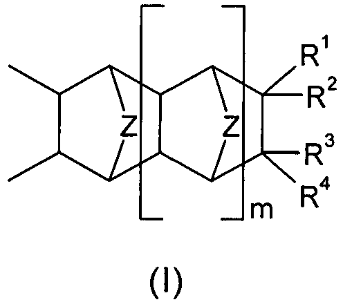
- Dispositif électronique organique selon la revendication 3, dans lequel le polymère polycyclooléfinique comprend un ou plusieurs types distincts d'unités de répétition de la formule I comprenant un groupe aryle ou aralkyle fluoré ou perfluoré pendant de la formule -(CH2)x-C6FyH5-y, et -(CH2)x-C6FyH4-y-pCzFqH2z+1-q, où x, y, q et z sont, de manière indépendante, respectivement choisis parmi des entiers de 0 à 5, de 0 à 5, de 0 à 9 et de 1 à 4, et "p" signifie "para".
- Dispositif électronique organique selon la revendication 3, dans lequel le polymère polycyclooléfinique comprend un ou plusieurs types distincts d'unités de répétition de la formule I qui sont formées par un ou plusieurs monomère(s) du type norbornène choisi(s) parmi le groupe constitué par les formules qui suivent :
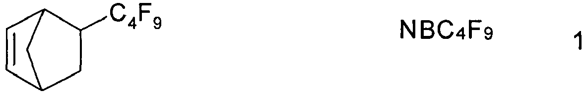
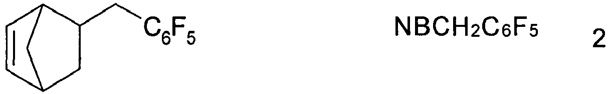


- Dispositif électronique organique selon une ou plusieurs des revendications 1 à 5, dans lequel le polymère polycyclooléfinique qui constitue la troisième couche comprend un groupe photoréactif ou réticulable comprenant une partie de liaison L et une partie fonctionnelle F, où L représente ou comprend un groupe choisi parmi les alkyles, les aralkyles, les aryles C1-C12 ou des analogues d'hétéroatomes, et F représente ou comprend un ou plusieurs corps chimiques pris parmi un maléimide, un 3-monoalkyl- ou 3,4-dialkylmaléimide, une moitié époxy, vinyle, acétylénique, cinnamate, indényle ou coumarine, qui est susceptible d'une réaction de réticulation ou de réticulation 2+2.
- Dispositif électronique organique selon une ou plusieurs des revendications 3 à 6, dans lequel le polymère polycyclooléfinique qui est contenu dans la troisième couche comprend un ou plusieurs types distincts d'unités de répétition de la formule I qui sont formées pendant la polymérisation à partir de monomères du type norbornène choisis parmi les formules qui suivent :


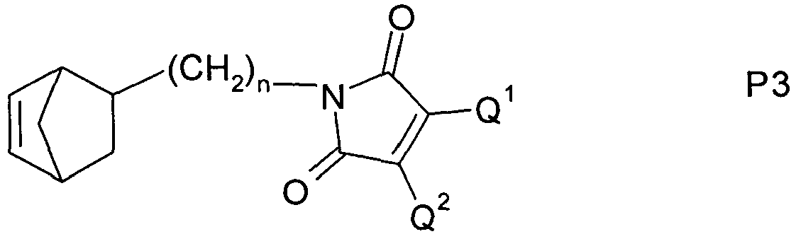
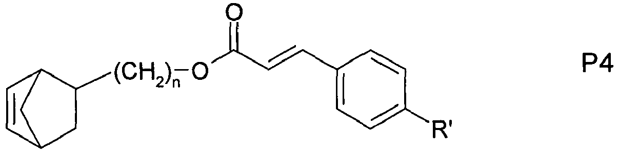


- Dispositif électronique organique selon une ou plusieurs des revendications 3 à 7, dans lequel le polymère polycyclooléfinique qui est contenu dans la troisième couche comprend un ou plusieurs types distincts d'unités de répétition de la formule I qui sont formées pendant la polymérisation à partir de monomères du type norbornène choisis parmi les formules qui suivent :
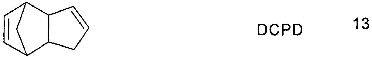


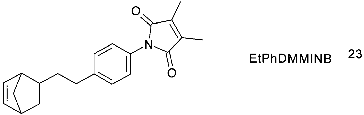


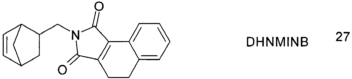


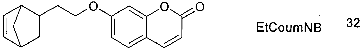


- Dispositif électronique organique selon une ou plusieurs des revendications 5 à 8, dans lequel le polymère polycyclooléfinique qui est contenue dans la troisième couche comprend un premier type d'unité de répétition choisie parmi les sous-formules 1, 2, 3, 4, 5, 6 et 12 comme défini selon la revendication 5 (NBC4F9, NBCH2C6F5, NBC6F5, NBCH2C6H3F2, NBCH2C6H4CF3, NBalkylC6F5 et PPVENB) et un second type d'unité de répétition choisie parmi les sous-formules 18, 19, 20, 21 et 22 comme défini selon la revendication 8 (DMMIMeNB, DMMIEtNB, DMMIPrNB, DMMIBuNB et DMMIHxNB).
- Dispositif électronique organique selon une ou plusieurs des revendications 1 à 9, dans lequel la deuxième couche comprend un fluoropolymère organique.
- Dispositif électronique organique selon une ou plusieurs des revendications 1 à 10, dans lequel les première, deuxième et troisième couches sont dérivées à partir d'une composition de polymère comprenant, en plus du polymère polycyclooléfinique ou du fluoropolymère, un ou plusieurs pris parmi un solvant, un agent de réticulation, un solvant réactif optionnel, un stabiliseur, un sensibiliseur UV, un agent favorisant l'adhérence et un sensibiliseur thermique.
- Dispositif électronique organique selon une ou plusieurs des revendications 1 à 11, dans lequel la première couche est préparée à partir d'une composition de polymère comprenant un polymère polycyclooléfinique et un solvant fluoré.
- Dispositif électronique organique selon une ou plusieurs des revendications 1 à 12, dans lequel la deuxième couche est préparée à partir d'une composition de polymère comprenant un fluoropolymère et un solvant fluoré.
- Dispositif électronique organique selon la revendication 12 ou 13, dans lequel le solvant fluoré est choisi parmi perfluorophénanthrène, perfluorodécaline, perfluoroperhydrofluorène, ou des mélanges des solvants mentionnés ci avant.
- Dispositif électronique organique selon une ou plusieurs des revendications 1 à 14, dans lequel la troisième couche est préparée à partir d'une composition de polymère comprenant un polymère polycyclooléfinique et un solvant organique non fluoré.
- Dispositif électronique organique selon la revendication 15, dans lequel le solvant organique non fluoré est choisi parmi propylène glycol monométhyl éther acétate (PGMEA), cyclopentanone, éthyl acétate, méthyl n-amyl cétone (MAK), méthyl éthyl cétone (MEK), diéthylène glycol butyl éther (DGBE) et xylène.
- Dispositif électronique organique selon une ou plusieurs des revendications 1 à 16, lequel est un transistor à effet de champ organique (OFET), un transistor à film mince organique (OTFT), une diode émettrice de lumière organique (OLED), un dispositif photovoltaïque organique (OPV) ou un photodétecteur organique (OPD).
- Dispositif électronique organique selon la revendication 17, lequel est un OFET à grille de sommet ou un OFET à grille de fond.
- OFET selon la revendication 18, lequel comprend un substrat (1), une électrode de grille (2), une couche diélectrique (3) jouant le rôle d'isolateur de grille, des électrodes de source et de drain (4a, 4b), une couche OSC (5) disposée sur les électrodes de source et de drain (4a, 4b), et une pile de couches de passivation comprenant des première (6a), deuxième (6b) et troisième (6c) couches de passivation comme défini selon une ou plusieurs des revendications 1 à 11.
- Procédé pour la préparation d'un OFET selon la revendication 19, lequel comprend les étapes qui suivent :a) formation d'une électrode de grille (2) sur un substrat (1),b) dépôt d'une couche en un matériau diélectrique (3) sur l'électrode de grille (2),c) formation d'électrodes de source et de drain (4a, 4b) sur la couche diélectrique (3),d) dépôt d'une couche en un matériau semiconducteur organique (OSC) (5) sur la couche diélectrique (3) et les électrodes de source et de drain (4a, 4b),e) dépôt d'une première couche de passivation (6a) comprenant un polymère polycyclooléfinique comprenant des groupes fluorés pendants sur la couche OSC (5),f) dépôt d'une deuxième couche de passivation (6b) comprenant un fluoropolymère sur la première couche de passivation (6a),g) dépôt d'une troisième couche de passivation (6c) comprenant des groupes fluorés pendants et des groupes réticulables pendants sur la deuxième couche de passivation (6b), réticulation des groupes réticulables pendants et en option, conformation de la troisième couche (6c).
- Produit ou assemblage comprenant un dispositif électronique organique selon une ou plusieurs des revendications 1 à 19, lequel est un circuit intégré (IC), une étiquette d'identification radiofréquence (RFID), un dispositif de marquage de sécurité ou de sécurité contenant une étiquette RFID, un affichage à écran plat (FPD), un plan arrière d'un FPD, un éclairage arrière d'un FPD, un dispositif électrophotographique, un dispositif d'enregistrement électrophotographique, un dispositif de mémoire organique, un capteur, un biocapteur ou une biopuce.
- Pile de couches de passivation dans un dispositif électronique organique, dans laquelle ladite pile de couches de passivation comprend des première, deuxième et troisième couches de passivation comme défini selon une ou plusieurs des revendications 1 à 16.
- Pile de couches de passivation selon la revendication 22, dans laquelle le dispositif électronique organique est un transistor à effet de champ organique (OFET), un transistor à film mince organique (OTFT), une diode émettrice de lumière organique (OLED), un dispositif photovoltaïque organique (OPV) ou un photodétecteur organique (OPD).
Priority Applications (1)
| Application Number | Priority Date | Filing Date | Title |
|---|---|---|---|
| EP13755966.2A EP2904648B1 (fr) | 2012-10-04 | 2013-08-22 | Couches de passivation pour dispositifs électroniques organiques |
Applications Claiming Priority (3)
| Application Number | Priority Date | Filing Date | Title |
|---|---|---|---|
| EP12006871 | 2012-10-04 | ||
| EP13755966.2A EP2904648B1 (fr) | 2012-10-04 | 2013-08-22 | Couches de passivation pour dispositifs électroniques organiques |
| PCT/EP2013/002536 WO2014053202A1 (fr) | 2012-10-04 | 2013-08-22 | Couches de passivation pour dispositifs électroniques organiques |
Publications (2)
| Publication Number | Publication Date |
|---|---|
| EP2904648A1 EP2904648A1 (fr) | 2015-08-12 |
| EP2904648B1 true EP2904648B1 (fr) | 2016-09-21 |
Family
ID=47048928
Family Applications (1)
| Application Number | Title | Priority Date | Filing Date |
|---|---|---|---|
| EP13755966.2A Not-in-force EP2904648B1 (fr) | 2012-10-04 | 2013-08-22 | Couches de passivation pour dispositifs électroniques organiques |
Country Status (4)
| Country | Link |
|---|---|
| US (1) | US9691985B2 (fr) |
| EP (1) | EP2904648B1 (fr) |
| TW (1) | TWI612126B (fr) |
| WO (1) | WO2014053202A1 (fr) |
Families Citing this family (14)
| Publication number | Priority date | Publication date | Assignee | Title |
|---|---|---|---|---|
| WO2016019277A1 (fr) | 2014-08-01 | 2016-02-04 | Orthogonal, Inc. | Formation de motifs photolithographique de dispositifs électroniques organiques |
| KR102401987B1 (ko) | 2014-08-01 | 2022-05-25 | 올싸거널 인코포레이티드 | 유기 전자 장치의 포토리소그래피 패터닝 |
| US10503065B2 (en) | 2014-08-01 | 2019-12-10 | Orthogonal, Inc. | Photolithographic patterning of devices |
| JP2017526177A (ja) | 2014-08-01 | 2017-09-07 | オーソゴナル,インコーポレイテッド | 素子のフォトリソグラフパターン化方法 |
| WO2016024823A1 (fr) * | 2014-08-14 | 2016-02-18 | 광주과학기술원 | Procede orthogonal de modelage de contours |
| WO2017052905A1 (fr) * | 2015-09-22 | 2017-03-30 | Applied Materials, Inc. | Appareil et procédé de dépôt sélectif |
| JP2019509638A (ja) * | 2016-03-31 | 2019-04-04 | ダウ グローバル テクノロジーズ エルエルシー | 不動態化薄膜トランジスタコンポーネント |
| KR102355529B1 (ko) * | 2017-08-07 | 2022-01-26 | 삼성디스플레이 주식회사 | 유기 전계 발광 표시 장치 |
| KR102358527B1 (ko) * | 2017-12-17 | 2022-02-08 | 어플라이드 머티어리얼스, 인코포레이티드 | 선택적 증착에 의한 실리사이드 막들 |
| KR20210028205A (ko) * | 2018-06-28 | 2021-03-11 | 메르크 파텐트 게엠베하 | 전자 디바이스의 제조 방법 |
| EP3904418A4 (fr) * | 2018-12-27 | 2022-09-14 | Mitsui Chemicals, Inc. | Copolymère de cyclo-oléfine pour dispositifs médicaux, composition de copolymère de cyclo-oléfine pour dispositifs médicaux, et corps moulé |
| KR102351155B1 (ko) * | 2020-01-30 | 2022-01-14 | 성균관대학교산학협력단 | 멀티 패시베이션을 이용한 인쇄 전자소자 제조 방법 및 인쇄 전자소자 |
| JP7547899B2 (ja) | 2020-09-28 | 2024-09-10 | 住友ベークライト株式会社 | ワニスおよび樹脂膜 |
| GB2631234A (en) * | 2023-06-21 | 2025-01-01 | Flexenable Tech Limited | Compound |
Family Cites Families (16)
| Publication number | Priority date | Publication date | Assignee | Title |
|---|---|---|---|---|
| GB1278780A (en) | 1968-12-24 | 1972-06-21 | Agfa Gevaert | Photodimerisation and photopolymerisation of bis-maleimides |
| US5468819A (en) | 1993-11-16 | 1995-11-21 | The B.F. Goodrich Company | Process for making polymers containing a norbornene repeating unit by addition polymerization using an organo (nickel or palladium) complex |
| GB9726810D0 (en) | 1997-12-19 | 1998-02-18 | Zeneca Ltd | Compounds composition & use |
| US6538087B2 (en) | 2000-07-28 | 2003-03-25 | Promerus, Llc | Polymeric compositions for forming optical waveguides; optical waveguides formed therefrom; and methods for making same |
| US6690029B1 (en) | 2001-08-24 | 2004-02-10 | University Of Kentucky Research Foundation | Substituted pentacenes and electronic devices made with substituted pentacenes |
| WO2003052841A1 (fr) | 2001-12-19 | 2003-06-26 | Avecia Limited | Transistor a effet de champ organique dote d'un dielectrique organique |
| US20060020068A1 (en) | 2004-07-07 | 2006-01-26 | Edmund Elce | Photosensitive compositions based on polycyclic polymers for low stress, high temperature films |
| US7674847B2 (en) | 2003-02-21 | 2010-03-09 | Promerus Llc | Vinyl addition polycyclic olefin polymers prepared with non-olefinic chain transfer agents and uses thereof |
| EP1687830B1 (fr) | 2003-11-28 | 2010-07-28 | Merck Patent GmbH | Ameliorations apportees a des couches semiconductrices organiques |
| EP1776498A4 (fr) | 2004-07-20 | 2014-04-23 | Lg Electronics Inc | Lave-linge et procede de commande de celui-ci |
| US7385221B1 (en) | 2005-03-08 | 2008-06-10 | University Of Kentucky Research Foundation | Silylethynylated heteroacenes and electronic devices made therewith |
| KR20070119671A (ko) * | 2005-03-11 | 2007-12-20 | 이 아이 듀폰 디 네모아 앤드 캄파니 | 광형상화가능, 열경화가능 불화 레지스트 |
| US8053515B2 (en) | 2006-12-06 | 2011-11-08 | Promerus Llc | Directly photodefinable polymer compositions and methods thereof |
| WO2011026550A1 (fr) * | 2009-09-05 | 2011-03-10 | Merck Patent Gmbh | Couches de passivation aptes à être traitées par une solution pour des dispositifs électroniques organiques |
| CN105440540A (zh) * | 2010-09-02 | 2016-03-30 | 默克专利股份有限公司 | 用于电子器件的夹层 |
| KR101839930B1 (ko) * | 2010-12-29 | 2018-04-27 | 삼성디스플레이 주식회사 | 유기 발광 표시 장치 및 유기 발광 표시 장치 제조 방법 |
-
2013
- 2013-08-22 US US14/433,083 patent/US9691985B2/en not_active Expired - Fee Related
- 2013-08-22 WO PCT/EP2013/002536 patent/WO2014053202A1/fr not_active Ceased
- 2013-08-22 EP EP13755966.2A patent/EP2904648B1/fr not_active Not-in-force
- 2013-10-03 TW TW102135902A patent/TWI612126B/zh not_active IP Right Cessation
Also Published As
| Publication number | Publication date |
|---|---|
| US20150280128A1 (en) | 2015-10-01 |
| EP2904648A1 (fr) | 2015-08-12 |
| WO2014053202A1 (fr) | 2014-04-10 |
| US9691985B2 (en) | 2017-06-27 |
| TW201425526A (zh) | 2014-07-01 |
| TWI612126B (zh) | 2018-01-21 |
Similar Documents
| Publication | Publication Date | Title |
|---|---|---|
| EP2904648B1 (fr) | Couches de passivation pour dispositifs électroniques organiques | |
| EP2841483B1 (fr) | Structures de bordure pour dispositifs électroniques organiques | |
| US9490439B2 (en) | Planarization layer for organic electronic devices | |
| US9923035B2 (en) | Method for producing organic electronic devices with bank structures, bank structures and electronic devices produced therewith | |
| EP2893575B1 (fr) | Procédé de modification de surface de structures diélectriques dans des dispositifs électroniques organiques | |
| KR102420851B1 (ko) | 유기 유전체층 및 유기 전자 장치 |
Legal Events
| Date | Code | Title | Description |
|---|---|---|---|
| PUAI | Public reference made under article 153(3) epc to a published international application that has entered the european phase |
Free format text: ORIGINAL CODE: 0009012 |
|
| 17P | Request for examination filed |
Effective date: 20150312 |
|
| AK | Designated contracting states |
Kind code of ref document: A1 Designated state(s): AL AT BE BG CH CY CZ DE DK EE ES FI FR GB GR HR HU IE IS IT LI LT LU LV MC MK MT NL NO PL PT RO RS SE SI SK SM TR |
|
| AX | Request for extension of the european patent |
Extension state: BA ME |
|
| DAX | Request for extension of the european patent (deleted) | ||
| GRAP | Despatch of communication of intention to grant a patent |
Free format text: ORIGINAL CODE: EPIDOSNIGR1 |
|
| INTG | Intention to grant announced |
Effective date: 20160429 |
|
| GRAS | Grant fee paid |
Free format text: ORIGINAL CODE: EPIDOSNIGR3 |
|
| GRAA | (expected) grant |
Free format text: ORIGINAL CODE: 0009210 |
|
| AK | Designated contracting states |
Kind code of ref document: B1 Designated state(s): AL AT BE BG CH CY CZ DE DK EE ES FI FR GB GR HR HU IE IS IT LI LT LU LV MC MK MT NL NO PL PT RO RS SE SI SK SM TR |
|
| REG | Reference to a national code |
Ref country code: GB Ref legal event code: FG4D |
|
| REG | Reference to a national code |
Ref country code: CH Ref legal event code: EP |
|
| REG | Reference to a national code |
Ref country code: AT Ref legal event code: REF Ref document number: 831668 Country of ref document: AT Kind code of ref document: T Effective date: 20161015 |
|
| REG | Reference to a national code |
Ref country code: IE Ref legal event code: FG4D |
|
| REG | Reference to a national code |
Ref country code: DE Ref legal event code: R096 Ref document number: 602013011889 Country of ref document: DE |
|
| REG | Reference to a national code |
Ref country code: LT Ref legal event code: MG4D Ref country code: NL Ref legal event code: MP Effective date: 20160921 |
|
| PG25 | Lapsed in a contracting state [announced via postgrant information from national office to epo] |
Ref country code: FI Free format text: LAPSE BECAUSE OF FAILURE TO SUBMIT A TRANSLATION OF THE DESCRIPTION OR TO PAY THE FEE WITHIN THE PRESCRIBED TIME-LIMIT Effective date: 20160921 Ref country code: RS Free format text: LAPSE BECAUSE OF FAILURE TO SUBMIT A TRANSLATION OF THE DESCRIPTION OR TO PAY THE FEE WITHIN THE PRESCRIBED TIME-LIMIT Effective date: 20160921 Ref country code: NO Free format text: LAPSE BECAUSE OF FAILURE TO SUBMIT A TRANSLATION OF THE DESCRIPTION OR TO PAY THE FEE WITHIN THE PRESCRIBED TIME-LIMIT Effective date: 20161221 Ref country code: LT Free format text: LAPSE BECAUSE OF FAILURE TO SUBMIT A TRANSLATION OF THE DESCRIPTION OR TO PAY THE FEE WITHIN THE PRESCRIBED TIME-LIMIT Effective date: 20160921 |
|
| REG | Reference to a national code |
Ref country code: AT Ref legal event code: MK05 Ref document number: 831668 Country of ref document: AT Kind code of ref document: T Effective date: 20160921 |
|
| PG25 | Lapsed in a contracting state [announced via postgrant information from national office to epo] |
Ref country code: NL Free format text: LAPSE BECAUSE OF FAILURE TO SUBMIT A TRANSLATION OF THE DESCRIPTION OR TO PAY THE FEE WITHIN THE PRESCRIBED TIME-LIMIT Effective date: 20160921 Ref country code: GR Free format text: LAPSE BECAUSE OF FAILURE TO SUBMIT A TRANSLATION OF THE DESCRIPTION OR TO PAY THE FEE WITHIN THE PRESCRIBED TIME-LIMIT Effective date: 20161222 Ref country code: LV Free format text: LAPSE BECAUSE OF FAILURE TO SUBMIT A TRANSLATION OF THE DESCRIPTION OR TO PAY THE FEE WITHIN THE PRESCRIBED TIME-LIMIT Effective date: 20160921 Ref country code: SE Free format text: LAPSE BECAUSE OF FAILURE TO SUBMIT A TRANSLATION OF THE DESCRIPTION OR TO PAY THE FEE WITHIN THE PRESCRIBED TIME-LIMIT Effective date: 20160921 |
|
| PG25 | Lapsed in a contracting state [announced via postgrant information from national office to epo] |
Ref country code: EE Free format text: LAPSE BECAUSE OF FAILURE TO SUBMIT A TRANSLATION OF THE DESCRIPTION OR TO PAY THE FEE WITHIN THE PRESCRIBED TIME-LIMIT Effective date: 20160921 Ref country code: RO Free format text: LAPSE BECAUSE OF FAILURE TO SUBMIT A TRANSLATION OF THE DESCRIPTION OR TO PAY THE FEE WITHIN THE PRESCRIBED TIME-LIMIT Effective date: 20160921 |
|
| PG25 | Lapsed in a contracting state [announced via postgrant information from national office to epo] |
Ref country code: BE Free format text: LAPSE BECAUSE OF FAILURE TO SUBMIT A TRANSLATION OF THE DESCRIPTION OR TO PAY THE FEE WITHIN THE PRESCRIBED TIME-LIMIT Effective date: 20160921 Ref country code: CZ Free format text: LAPSE BECAUSE OF FAILURE TO SUBMIT A TRANSLATION OF THE DESCRIPTION OR TO PAY THE FEE WITHIN THE PRESCRIBED TIME-LIMIT Effective date: 20160921 Ref country code: SM Free format text: LAPSE BECAUSE OF FAILURE TO SUBMIT A TRANSLATION OF THE DESCRIPTION OR TO PAY THE FEE WITHIN THE PRESCRIBED TIME-LIMIT Effective date: 20160921 Ref country code: BG Free format text: LAPSE BECAUSE OF FAILURE TO SUBMIT A TRANSLATION OF THE DESCRIPTION OR TO PAY THE FEE WITHIN THE PRESCRIBED TIME-LIMIT Effective date: 20161221 Ref country code: AT Free format text: LAPSE BECAUSE OF FAILURE TO SUBMIT A TRANSLATION OF THE DESCRIPTION OR TO PAY THE FEE WITHIN THE PRESCRIBED TIME-LIMIT Effective date: 20160921 Ref country code: SK Free format text: LAPSE BECAUSE OF FAILURE TO SUBMIT A TRANSLATION OF THE DESCRIPTION OR TO PAY THE FEE WITHIN THE PRESCRIBED TIME-LIMIT Effective date: 20160921 Ref country code: PL Free format text: LAPSE BECAUSE OF FAILURE TO SUBMIT A TRANSLATION OF THE DESCRIPTION OR TO PAY THE FEE WITHIN THE PRESCRIBED TIME-LIMIT Effective date: 20160921 Ref country code: PT Free format text: LAPSE BECAUSE OF FAILURE TO SUBMIT A TRANSLATION OF THE DESCRIPTION OR TO PAY THE FEE WITHIN THE PRESCRIBED TIME-LIMIT Effective date: 20170123 Ref country code: ES Free format text: LAPSE BECAUSE OF FAILURE TO SUBMIT A TRANSLATION OF THE DESCRIPTION OR TO PAY THE FEE WITHIN THE PRESCRIBED TIME-LIMIT Effective date: 20160921 Ref country code: IS Free format text: LAPSE BECAUSE OF FAILURE TO SUBMIT A TRANSLATION OF THE DESCRIPTION OR TO PAY THE FEE WITHIN THE PRESCRIBED TIME-LIMIT Effective date: 20170121 |
|
| REG | Reference to a national code |
Ref country code: DE Ref legal event code: R097 Ref document number: 602013011889 Country of ref document: DE |
|
| PG25 | Lapsed in a contracting state [announced via postgrant information from national office to epo] |
Ref country code: IT Free format text: LAPSE BECAUSE OF FAILURE TO SUBMIT A TRANSLATION OF THE DESCRIPTION OR TO PAY THE FEE WITHIN THE PRESCRIBED TIME-LIMIT Effective date: 20160921 |
|
| REG | Reference to a national code |
Ref country code: FR Ref legal event code: PLFP Year of fee payment: 5 |
|
| PLBE | No opposition filed within time limit |
Free format text: ORIGINAL CODE: 0009261 |
|
| STAA | Information on the status of an ep patent application or granted ep patent |
Free format text: STATUS: NO OPPOSITION FILED WITHIN TIME LIMIT |
|
| PG25 | Lapsed in a contracting state [announced via postgrant information from national office to epo] |
Ref country code: DK Free format text: LAPSE BECAUSE OF FAILURE TO SUBMIT A TRANSLATION OF THE DESCRIPTION OR TO PAY THE FEE WITHIN THE PRESCRIBED TIME-LIMIT Effective date: 20160921 |
|
| 26N | No opposition filed |
Effective date: 20170622 |
|
| PG25 | Lapsed in a contracting state [announced via postgrant information from national office to epo] |
Ref country code: SI Free format text: LAPSE BECAUSE OF FAILURE TO SUBMIT A TRANSLATION OF THE DESCRIPTION OR TO PAY THE FEE WITHIN THE PRESCRIBED TIME-LIMIT Effective date: 20160921 |
|
| REG | Reference to a national code |
Ref country code: CH Ref legal event code: PL |
|
| PG25 | Lapsed in a contracting state [announced via postgrant information from national office to epo] |
Ref country code: MC Free format text: LAPSE BECAUSE OF FAILURE TO SUBMIT A TRANSLATION OF THE DESCRIPTION OR TO PAY THE FEE WITHIN THE PRESCRIBED TIME-LIMIT Effective date: 20160921 |
|
| PG25 | Lapsed in a contracting state [announced via postgrant information from national office to epo] |
Ref country code: LI Free format text: LAPSE BECAUSE OF NON-PAYMENT OF DUE FEES Effective date: 20170831 Ref country code: CH Free format text: LAPSE BECAUSE OF NON-PAYMENT OF DUE FEES Effective date: 20170831 |
|
| REG | Reference to a national code |
Ref country code: IE Ref legal event code: MM4A |
|
| PG25 | Lapsed in a contracting state [announced via postgrant information from national office to epo] |
Ref country code: LU Free format text: LAPSE BECAUSE OF NON-PAYMENT OF DUE FEES Effective date: 20170822 |
|
| REG | Reference to a national code |
Ref country code: FR Ref legal event code: PLFP Year of fee payment: 6 |
|
| PG25 | Lapsed in a contracting state [announced via postgrant information from national office to epo] |
Ref country code: IE Free format text: LAPSE BECAUSE OF NON-PAYMENT OF DUE FEES Effective date: 20170822 |
|
| PG25 | Lapsed in a contracting state [announced via postgrant information from national office to epo] |
Ref country code: MT Free format text: LAPSE BECAUSE OF NON-PAYMENT OF DUE FEES Effective date: 20170822 |
|
| PG25 | Lapsed in a contracting state [announced via postgrant information from national office to epo] |
Ref country code: AL Free format text: LAPSE BECAUSE OF FAILURE TO SUBMIT A TRANSLATION OF THE DESCRIPTION OR TO PAY THE FEE WITHIN THE PRESCRIBED TIME-LIMIT Effective date: 20160921 |
|
| PG25 | Lapsed in a contracting state [announced via postgrant information from national office to epo] |
Ref country code: HU Free format text: LAPSE BECAUSE OF FAILURE TO SUBMIT A TRANSLATION OF THE DESCRIPTION OR TO PAY THE FEE WITHIN THE PRESCRIBED TIME-LIMIT; INVALID AB INITIO Effective date: 20130822 |
|
| PG25 | Lapsed in a contracting state [announced via postgrant information from national office to epo] |
Ref country code: CY Free format text: LAPSE BECAUSE OF FAILURE TO SUBMIT A TRANSLATION OF THE DESCRIPTION OR TO PAY THE FEE WITHIN THE PRESCRIBED TIME-LIMIT Effective date: 20160921 |
|
| PG25 | Lapsed in a contracting state [announced via postgrant information from national office to epo] |
Ref country code: MK Free format text: LAPSE BECAUSE OF FAILURE TO SUBMIT A TRANSLATION OF THE DESCRIPTION OR TO PAY THE FEE WITHIN THE PRESCRIBED TIME-LIMIT Effective date: 20160921 |
|
| PG25 | Lapsed in a contracting state [announced via postgrant information from national office to epo] |
Ref country code: TR Free format text: LAPSE BECAUSE OF FAILURE TO SUBMIT A TRANSLATION OF THE DESCRIPTION OR TO PAY THE FEE WITHIN THE PRESCRIBED TIME-LIMIT Effective date: 20160921 |
|
| REG | Reference to a national code |
Ref country code: GB Ref legal event code: 732E Free format text: REGISTERED BETWEEN 20200312 AND 20200318 |
|
| PG25 | Lapsed in a contracting state [announced via postgrant information from national office to epo] |
Ref country code: HR Free format text: LAPSE BECAUSE OF FAILURE TO SUBMIT A TRANSLATION OF THE DESCRIPTION OR TO PAY THE FEE WITHIN THE PRESCRIBED TIME-LIMIT Effective date: 20160921 |
|
| PGFP | Annual fee paid to national office [announced via postgrant information from national office to epo] |
Ref country code: GB Payment date: 20200813 Year of fee payment: 8 Ref country code: DE Payment date: 20200812 Year of fee payment: 8 Ref country code: FR Payment date: 20200715 Year of fee payment: 8 |
|
| REG | Reference to a national code |
Ref country code: DE Ref legal event code: R119 Ref document number: 602013011889 Country of ref document: DE |
|
| GBPC | Gb: european patent ceased through non-payment of renewal fee |
Effective date: 20210822 |
|
| PG25 | Lapsed in a contracting state [announced via postgrant information from national office to epo] |
Ref country code: GB Free format text: LAPSE BECAUSE OF NON-PAYMENT OF DUE FEES Effective date: 20210822 Ref country code: FR Free format text: LAPSE BECAUSE OF NON-PAYMENT OF DUE FEES Effective date: 20210831 Ref country code: DE Free format text: LAPSE BECAUSE OF NON-PAYMENT OF DUE FEES Effective date: 20220301 |
|
| P01 | Opt-out of the competence of the unified patent court (upc) registered |
Effective date: 20230528 |