EP2905672A1 - Vorrichtung und Verfahren für eine gewünschte Brokaw-Bandlückenreferenzschaltung für verbesserte Niederspannungsversorgung - Google Patents
Vorrichtung und Verfahren für eine gewünschte Brokaw-Bandlückenreferenzschaltung für verbesserte Niederspannungsversorgung Download PDFInfo
- Publication number
- EP2905672A1 EP2905672A1 EP14368016.3A EP14368016A EP2905672A1 EP 2905672 A1 EP2905672 A1 EP 2905672A1 EP 14368016 A EP14368016 A EP 14368016A EP 2905672 A1 EP2905672 A1 EP 2905672A1
- Authority
- EP
- European Patent Office
- Prior art keywords
- bipolar transistor
- npn bipolar
- resistor
- electrically connected
- voltage
- Prior art date
- Legal status (The legal status is an assumption and is not a legal conclusion. Google has not performed a legal analysis and makes no representation as to the accuracy of the status listed.)
- Withdrawn
Links
- 238000000034 method Methods 0.000 title claims abstract description 13
- 230000001419 dependent effect Effects 0.000 claims abstract description 5
- 229910000577 Silicon-germanium Inorganic materials 0.000 claims description 4
- 238000012358 sourcing Methods 0.000 claims description 3
- JBRZTFJDHDCESZ-UHFFFAOYSA-N AsGa Chemical compound [As]#[Ga] JBRZTFJDHDCESZ-UHFFFAOYSA-N 0.000 claims description 2
- GPXJNWSHGFTCBW-UHFFFAOYSA-N Indium phosphide Chemical compound [In]#P GPXJNWSHGFTCBW-UHFFFAOYSA-N 0.000 claims description 2
- AXQKVSDUCKWEKE-UHFFFAOYSA-N [C].[Ge].[Si] Chemical compound [C].[Ge].[Si] AXQKVSDUCKWEKE-UHFFFAOYSA-N 0.000 claims description 2
- LEVVHYCKPQWKOP-UHFFFAOYSA-N [Si].[Ge] Chemical compound [Si].[Ge] LEVVHYCKPQWKOP-UHFFFAOYSA-N 0.000 claims description 2
- 239000002019 doping agent Substances 0.000 claims 2
- 102000004213 Neuropilin-2 Human genes 0.000 description 38
- 108090000770 Neuropilin-2 Proteins 0.000 description 38
- 102000004207 Neuropilin-1 Human genes 0.000 description 36
- 108090000772 Neuropilin-1 Proteins 0.000 description 36
- 101000704557 Homo sapiens Sulfiredoxin-1 Proteins 0.000 description 7
- 102100031797 Sulfiredoxin-1 Human genes 0.000 description 7
- XUIMIQQOPSSXEZ-UHFFFAOYSA-N Silicon Chemical compound [Si] XUIMIQQOPSSXEZ-UHFFFAOYSA-N 0.000 description 5
- 238000005516 engineering process Methods 0.000 description 5
- 229910052710 silicon Inorganic materials 0.000 description 5
- 239000010703 silicon Substances 0.000 description 5
- 230000007423 decrease Effects 0.000 description 2
- 230000006872 improvement Effects 0.000 description 2
- 230000003071 parasitic effect Effects 0.000 description 2
- 239000004065 semiconductor Substances 0.000 description 2
- GYHNNYVSQQEPJS-UHFFFAOYSA-N Gallium Chemical compound [Ga] GYHNNYVSQQEPJS-UHFFFAOYSA-N 0.000 description 1
- 230000008859 change Effects 0.000 description 1
- 230000000295 complement effect Effects 0.000 description 1
- 230000008878 coupling Effects 0.000 description 1
- 238000010168 coupling process Methods 0.000 description 1
- 238000005859 coupling reaction Methods 0.000 description 1
- 230000000694 effects Effects 0.000 description 1
- 230000005684 electric field Effects 0.000 description 1
- 229910052733 gallium Inorganic materials 0.000 description 1
- 238000012986 modification Methods 0.000 description 1
- 230000004048 modification Effects 0.000 description 1
- 230000008569 process Effects 0.000 description 1
- 230000010076 replication Effects 0.000 description 1
- 230000004044 response Effects 0.000 description 1
Images

Classifications
-
- G—PHYSICS
- G05—CONTROLLING; REGULATING
- G05F—SYSTEMS FOR REGULATING ELECTRIC OR MAGNETIC VARIABLES
- G05F3/00—Non-retroactive systems for regulating electric variables by using an uncontrolled element, or an uncontrolled combination of elements, such element or such combination having self-regulating properties
- G05F3/02—Regulating voltage or current
- G05F3/08—Regulating voltage or current wherein the variable is DC
- G05F3/10—Regulating voltage or current wherein the variable is DC using uncontrolled devices with non-linear characteristics
- G05F3/16—Regulating voltage or current wherein the variable is DC using uncontrolled devices with non-linear characteristics being semiconductor devices
-
- G—PHYSICS
- G05—CONTROLLING; REGULATING
- G05F—SYSTEMS FOR REGULATING ELECTRIC OR MAGNETIC VARIABLES
- G05F1/00—Automatic systems in which deviations of an electric quantity from one or more predetermined values are detected at the output of the system and fed back to a device within the system to restore the detected quantity to its predetermined value or values, i.e. retroactive systems
- G05F1/10—Regulating voltage or current
-
- G—PHYSICS
- G05—CONTROLLING; REGULATING
- G05F—SYSTEMS FOR REGULATING ELECTRIC OR MAGNETIC VARIABLES
- G05F3/00—Non-retroactive systems for regulating electric variables by using an uncontrolled element, or an uncontrolled combination of elements, such element or such combination having self-regulating properties
- G05F3/02—Regulating voltage or current
- G05F3/08—Regulating voltage or current wherein the variable is DC
- G05F3/10—Regulating voltage or current wherein the variable is DC using uncontrolled devices with non-linear characteristics
- G05F3/16—Regulating voltage or current wherein the variable is DC using uncontrolled devices with non-linear characteristics being semiconductor devices
- G05F3/20—Regulating voltage or current wherein the variable is DC using uncontrolled devices with non-linear characteristics being semiconductor devices using diode- transistor combinations
- G05F3/22—Regulating voltage or current wherein the variable is DC using uncontrolled devices with non-linear characteristics being semiconductor devices using diode- transistor combinations wherein the transistors are of the bipolar type only
-
- G—PHYSICS
- G05—CONTROLLING; REGULATING
- G05F—SYSTEMS FOR REGULATING ELECTRIC OR MAGNETIC VARIABLES
- G05F3/00—Non-retroactive systems for regulating electric variables by using an uncontrolled element, or an uncontrolled combination of elements, such element or such combination having self-regulating properties
- G05F3/02—Regulating voltage or current
- G05F3/08—Regulating voltage or current wherein the variable is DC
- G05F3/10—Regulating voltage or current wherein the variable is DC using uncontrolled devices with non-linear characteristics
- G05F3/16—Regulating voltage or current wherein the variable is DC using uncontrolled devices with non-linear characteristics being semiconductor devices
- G05F3/20—Regulating voltage or current wherein the variable is DC using uncontrolled devices with non-linear characteristics being semiconductor devices using diode- transistor combinations
- G05F3/30—Regulators using the difference between the base-emitter voltages of two bipolar transistors operating at different current densities
Definitions
- the disclosure relates generally to a bandgap reference circuit and, more particularly, to a bandgap reference circuit device for a low voltage power supply thereof.
- Bandgap reference circuits are a type of voltage reference circuit used in conjunction with semiconductor devices, integrated circuits (IC), and other applications. The requirement for a stable reference voltage is universal in electronic design. Using a two transistor circuit , collector current sensing can provide minimization of errors due to the base current.
- a bandgap voltage reference circuit the voltage difference between two p-n junctions (e.g. diodes, or bipolar transistors), operated at different current densities, can be used to generate a proportional to absolute temperature (PTAT) current in a first resistor. This current can then be used to generate a voltage in a second resistor. This voltage, in turn, is added to the voltage of one of the junctions.
- PTAT proportional to absolute temperature
- the voltage across a diode operated at a constant current, or herewith a PTAT current, is complementary to absolute temperature (CTAT). If the ratio between the first and second resistor is chosen properly, the first order effects of the temperature dependency of the diode and the PTAT current will cancel out. In this fashion, a circuit can be independent of temperature variation, and provide a constant voltage reference.
- bandgap voltage reference circuits Circuits of this nature that are temperature insensitive are referred to as bandgap voltage reference circuits.
- the resulting voltage is about 1.2-1.3V, depending on the particular technology and circuit design, and is close to the theoretical silicon bandgap voltage of 1.22 eV at 0 degrees Kelvin.
- the remaining voltage change over the operating temperature of typical integrated circuits is on the order of a few millivolts. Because the output voltage is by definition fixed around 1.25V for typical bandgap reference circuits, the minimum operating voltage is about 1.4V.
- a circuit implementation that has this characteristic is called a Brokaw bandgap reference circuit.
- the Brokaw bandgap reference circuit is a voltage reference circuit that is widely used in integrated circuit technology to establish a voltage reference.
- the Brokaw bandgap reference circuit has an output voltage of sapproximately 1.25V, and has very little temperature dependence.
- the circuit maintains an internal voltage source that has a positive temperature coefficient (PTC) and another internal voltage source that has a negative temperature coefficient (NTC). By summing the two together, the temperature dependence can be canceled. Additionally, either of the two internal sources can be used as a temperature sensor.
- PTC positive temperature coefficient
- NTC negative temperature coefficient
- the circuit uses negative feedback to force a constant current through two bipolar transistors with different emitter areas.
- the transistor with the larger emitter area requires a smaller base-emitter voltage, V BE , (e.g. or Vbe) for the same current.
- V BE base-emitter voltage
- the base-emitter voltage for each transistor has a negative temperature coefficient (i.e., it decreases with temperature).
- the difference between the two base-emitter voltages has a positive temperature coefficient (i.e., it increases with temperature). With proper component choices, the two opposing temperature coefficients will cancel each other exactly and the output will have no temperature dependence.
- FIG. 1 shows the circuit schematic for the Brokaw bandgap circuit.
- the circuit is powered using a VDD power supply 10, and ground power supply 20.
- the output of the circuit is VREF 30.
- the circuit contains a first npn bipolar transistor, NPN1 70, and a second npn bipolar transistor, NPN2, 80.
- the circuit network contains a first resistor R1 90, and a second resistor R2 95 to provide a feedback network.
- a first p-channel MOSFET, PMOS1, 40 and second p-channel MOSFET , PMOS2 50 serve as current sources for the NPN1 70 and NPN2 80 transistors, respectively.
- a third p-channel MOSFET, PMOS3 60 and resistor R3 100 are provided for the output voltage reference.
- the base-emitter voltage of NPN 1 70 is referred to as Vbe1.
- the base-emitter voltage of NPN2 80 is referred to as Vbe2.
- the voltage drop across first resistor R1 90 is kT/q In ⁇ J1/J2 ⁇ where J1 and J2 is the current density flowing through NPN1 70, and NPN2 80, respectively.
- the voltage drop across second resistor R2 95 is equal to 2 (R2/R1) ⁇ kT/q ⁇ In ⁇ J1/J2 ⁇ .
- the first and second npn bipolar transistors, NPN1 70 and NPN2 80, are of different physical size.
- the voltage drop, the voltage drop across the resistor R1 90 is small, the larger area of NPN2 causes it conduct more of the total current available through R2 95.
- the resulting imbalance in collector voltages drives the op amp so as to raise the base voltage.
- a large current is forced through R2 95 leading to a voltage drop across R1 90 will limit the current flow through NPN2 80.
- a base voltage at which the collector currents match is a base voltage at which the collector currents match.
- the npn layout of NPN1 70 and NPN2 80 can have different "emitter finger” numbers to establish different physical bipolar transistor sizes. This can be designated by 1:M, indicating the ratio of emitter fingers of 1 in NPN1 70 and multiplicity of M in NPN2 80.
- the differential voltage, ⁇ Vbe is proportional to the current flowing through the NPN1 70 and NPN2 80.
- the collector current flowing through collector of NPN1 70 is equal to the current flowing through PMOS1 40.
- the collector current flowing through NPN2 80 is equal to the current flowing through PMOS2 50. Therefore, PMOS1 40 and PMOS2 50 current ratio is proportional to "delta" Vbe voltage, which is proportional to absolute temperature (PTAT). Assuming the resistor ratio and current density ratio are invariant, the voltage varies directly with absolute temperature T.
- the base of NPN1 70 and NPN2 80 are electrically connected, providing a common base voltage condition.
- the base voltage of NPN1 70 and NPN2 80 base (which are connected) can be calculated according to the following R ⁇ 2 ⁇ ⁇ ⁇ Vbe R ⁇ 1 + Vbe
- the Delta Vbe, ⁇ Vbe (also denoted as D Vbe), and Vbe can cancel out the temperature coefficient, because ⁇ Vbe has a positive temperature coefficient (PTC) and Vbe has a negative temperature coefficient (NTC) and creates the temperature independent, so-called bandgap voltage.
- PTC positive temperature coefficient
- NTC negative temperature coefficient
- bandgap voltage so-called bandgap voltage.
- the utilization of the transistor base-emitter diode temperature compensated to the bandgap voltage of silicon is a technique to establish the bandgap voltage. This is usually becomes approximately ⁇ 1.2V.
- the common base voltage, V B , of NPN1 70 and NPN2 80 is approximately -1.2V. Therefore, the collector voltage of NPN1 70 should be higher than the value of ⁇ 1.2V.
- the p-channel MOSFET, PMOS1 source and gate voltage needs to be more than a threshold voltage of a PMOS transistor, which usually more than 0.4V-0.7V; in addition, some additional voltage is desirable to provide good matching of PMOS1 40 and PMOS2 50. Therefore, in this case, the supply voltage must be more than 1.6V. Additionally, a supply voltage of more than 2V is desirable in this circuit. It is difficult to make this circuit operable in ideally, a 1.5V power supply voltage range.
- the power supply voltage, V DD continues to decrease to maintain dielectric reliability.
- the native power supply voltage or internal power supply voltage
- the Brokaw bandgap reference does not provide desirable operability, or ideal operating characteristics. For technologies whose minimum dimension is below 0.13 ⁇ m, the issue is also a concern.
- Brokaw style bandgap voltage regulator comprising a that comprise of bipolar current mirror, resistor divider networks and a bipolar output device.
- bandgap circuits on the order of 1V have been discussed.
- a bandgap circuit topology allows for function at low power supply voltages, on the order of 1 V.
- the circuit has a replication circuit , and an output stage containing a current mirror.
- the solution to improve the operability of a low voltage bandgap circuit utilized various alternative solutions.
- a principal object of the present disclosure is to provide a circuit which allows for operation of a modified Brokaw bandgap circuit for low power supply voltages.
- a principal object of the present disclosure is to provide a bandgap circuit which allows operation for power supply voltages below 2V.
- a principal object of the present disclosure is to provide a bandgap circuit that sets the NPN base voltage lower than the bandgap voltage ( ⁇ 1.2V ).
- Another further object of the present disclosure is to provide a bandgap circuit and add the voltage to create the bandgap voltage in another branch.
- a bandgap voltage reference circuit between a power supply node and a ground node and configured for generating a reference voltage, comprising of a bandgap voltage network providing a base emitter voltage, a feedback network providing feedback function to a bandgap voltage network, a current mirror sourcing said bandgap voltage network, and an output network function providing a lower stabilized output voltage.
- a band gap voltage reference circuit with improved operation at low voltage power supply comprising a first npn bipolar transistor, a second npn bipolar transistor wherein the base of the second npn bipolar transistor and first npn bipolar transistor are electrically coupled providing a differential voltage in the base-emitter voltage, a third npn bipolar transistor wherein the base of the third npn bipolar transistor is electrically connected to the base of said first npn bipolar transistor and electrically connected to the collector of the third npn bipolar transistor, a first resistor element electrically connected to the emitter of the second npn bipolar transistor, a second resistor element electrically connected to the emitter of the first npn bipolar transistor, a third resistor element electrically connected to the emitter of the third npn bipolar transistor, a fourth resistor element electrically connected to the collector of the third npn bipolar transistor, a first p-channel MOSFET wherein the
- a bandgap voltage reference circuit with improved operation at low voltage power supply, the circuit comprising a a first npn bipolar transistor, a second npn bipolar transistor wherein the base of the second npn bipolar transistor and first npn bipolar transistor are electrically coupled, a third npn bipolar transistor wherein the base of the third npn bipolar transistor is electrically connected to the base of the first npn bipolar transistor and electrically connected to the collector of the third npn bipolar transistor, a first resistor element electrically connected to the emitter of the second npn bipolar transistor, a second resistor element electrically connected to the emitter of the first npn bipolar transistor, a third resistor element electrically connected to the emitter of said third npn bipolar transistor, a fourth resistor element electrically connected to the collector of the third npn bipolar transistor, a first pnp bipolar transistor wherein the first pnp bipolar transistor base and collector are electrically
- a method of a bandgap voltage reference circuit is comprising the following steps: a first step providing a first npn bipolar transistor, a second npn bipolar transistor, a third npn bipolar transistor, a first resistor, a second resistor, a third resistor, a fourth resistor, and a first, second and third p-channel MOSFET ; a second step forming a emitter ratio of 1:M for the first and said second npn bipolar transistors ; a third step matching the second resistor and the third resistor ; a fourth step establishing a ⁇ Vbe dependent current from the first and third npn bipolar transistor; a fifth step establishing a ⁇ Vbe with the fourth resistor; and lastly, a sixth step calculating a bandgap output voltage as a function of of Vbe, ⁇ Vbe, and the first resistor, said third resistor, and the fourth resistor.
- FIG. 1 is a prior art example of a Brokaw bandgap circuit in accordance with a prior art embodiment.
- the circuit is powered using a VDD power supply 10, and ground power supply 20.
- the output of the circuit is VREF 30.
- the circuit contains a first npn bipolar transistor, NPN1 70, and a second npn bipolar transistor, NPN2, 80.
- the circuit network contains a first resistor R1 90, and a second resistor R2 95 to provide a feedback network.
- a first p-channel MOSFET, PMOS1, 40 and second p-channel MOSFET , PMOS2 50 serve as current sources for the NPN1 70 and NPN2 80 transistors, respectively.
- a third p-channel MOSFET, PMOS3 60 and resistor R3 100 are provided.
- the base-emitter voltage of NPN 1 70 is referred to as Vbe1.
- the base-emitter voltage of NPN2 80 is referred to as Vbe2.
- the voltage drop across first resistor R1 90 is kT/q In ⁇ J1/J2 ⁇ where J1 and J2 is the current density flowing through NPN1 70, and NPN2 80, respectively.
- the voltage drop across second resistor R2 95 is equal to 2 (R2/R1) ⁇ kT/q ⁇ In ⁇ J1/J2 ⁇ .
- the first and second npn bipolar transistors, NPN1 70 and NPN2 80, are of different physical size.
- the voltage drop, the voltage drop across the resistor R1 90 is small, the larger area of NPN2 causes it conduct more of the total current available through R2 95.
- the resulting imbalance in collector voltages drives the op amp so as to raise the base voltage.
- a large current is forced through R2 95 leading to a voltage drop across R1 90 will limit the current flow through NPN2 80.
- a base voltage at which the collector currents match is a base voltage at which the collector currents match.
- the npn layout of NPN1 70 and NPN2 80 can have different "emitter finger” numbers to establish different physical bipolar transistor sizes. This can be designated by 1:M, indicating the ratio of emitter fingers of 1 in NPN1 70 and multiplicity of M in NPN2 80.
- the two transistors establish a differential voltage in the base-emitter voltage, referred to as a so-called “delta Vbe voltage” ( ⁇ Vbe), .
- ⁇ Vbe kT / q ⁇ ln J ⁇ 1 / J ⁇ 2
- the differential voltage, ⁇ Vbe is proportional to the current flowing through the NPN1 70 and NPN2 80.
- the collector current flowing through collector of NPN1 70 is equal to the current flowing through PMOS1 40.
- the collector current flowing through NPN2 80 is equal to the current flowing through PMOS2 50. Therefore, PMOS1 40 and PMOS2 50 current ratio is proportional to "delta" Vbe voltage, which is proportional to absolute temperature (PTAT). Assuming the resistor ratio and current density ratio are invariant, the voltage varies directly with absolute temperature T.
- the base of NPN1 70 and NPN2 80 are electrically connected, providing a common base voltage condition.
- the base voltage of NPN1 70 and NPN2 80 base (which are connected) can be calculated according to the following R ⁇ 2 ⁇ ⁇ ⁇ Vbe R ⁇ 1 + Vbe .
- the Delta Vbe, ⁇ Vbe (also denoted as D Vbe), and Vbe can cancel out the temperature coefficient, because ⁇ Vbe has a positive temperature coefficient (PTC) and Vbe has a negative temperature coefficient (NTC) and creates the temperature independent, so-called bandgap voltage.
- PTC positive temperature coefficient
- NTC negative temperature coefficient
- the utilization of the transistor base-emitter diode temperature compensated to the bandgap voltage of silicon is a technique to establish the bandgap voltage. This is usually becomes approximately ⁇ 1.2V.
- the common base voltage, V B , of NPN1 70 and NPN2 80 is approximately ⁇ 1.2V. Therefore, the collector voltage of NPN1 70 should be higher than the value of ⁇ 1.2V.
- the p-channel MOSFET, PMOS1 source and gate voltage needs to be more than a threshold voltage of a PMOS transistor, which usually more than 0.4V-0.7V; in addition, some additional voltage is desirable to provide good matching of PMOS1 40 and PMOS2 50. Therefore, in this case, the supply voltage must be more than 1.6V. Additionally, a supply voltage of more than 2V is desirable in this circuit. It is difficult to make this circuit operable in ideally, a 1.5V power supply voltage range.
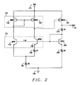
- FIG. 2 is a circuit schematic of an modified Brokaw bandgap circuit in accordance with an embodiment of the disclosure.
- a modified Brokaw bandgap voltage reference circuit is between a power supply node and a ground node and configured for generating a reference voltage, comprising of a bandgap voltage network providing a base emitter voltage, a feedback network providing feedback function to a bandgap voltage network, a current mirror sourcing said bandgap voltage network, and an output network function providing a lower stabilized output voltage.
- the circuit is powered using a VDD power supply 110, and ground power supply 120.
- the output of the circuit is VREF 130.
- the circuit contains a first npn bipolar transistor, NPN1 170, and a second npn bipolar transistor, NPN2, 180.
- This network 175 forms a a bandgap voltage network providing a base emitter voltage.
- the circuit network contains a first resistor R1 190, and a second resistor R2 195 to provide a feedback network providing feedback function to a bandgap voltage network,
- a first p-channel MOSFET, PMOS1,140 and second p-channel MOSFET , PMOS2 150 form a current mirror 145, and serves as current sources for the NPN170 and NPN2 180 transistors, respectively.
- a third p-channel MOSFET, PMOS3 160 and resistor R3 200 are provided for the output voltage reference.
- the output network function provides a lower stabilized output voltage.
- an additional npn bipolar transistor NPN3 220 is configured in a current mirror configuration with the parallel combination of NPN1 170 and NPN2 180, electrically coupling the npn base regions of NPN1 170, NPN2 180 and NPN3 220.
- the NPN3 220 has its base and collector electrically connected to establish the current mirror response.
- a resistor element R4 210 is electrically connected between NPN3 220 and PMOS 3 160.
- the first and second npn bipolar transistors, NPN1 170 and NPN2 180 are of different physical size.
- the npn layouts of NPN1 170 and NPN2 180 can be of different "emitter finger" numbers to establish different physical bipolar transistor sizes. This can be designated by 1:M, indicating the ratio of emitter fingers of 1 in NPN1 170 and a multiplicity of M fingers in NPN2 180.
- the two transistors establish a differential voltage in the base-emitter voltage, referred to as so-called “delta Vbe voltage" ( ⁇ Vbe). This establishes a ⁇ Vbe between resistor R1 190 by the feedback. Therefore, PMOS1 140 and PMOS2 150 current is proportional to "delta" Vbe voltage, which is proportional to absolute temperature (PTAT).
- the base of NPN1 170, the base of NPN2 80, and the base of NPN3 are electrically connected, providing a common base voltage condition.
- the base voltage of NPN1 170, NPN2 180 and NPN3 220 base (which are connected) can be calculated according to the following R ⁇ 2 ⁇ ⁇ ⁇ Vbe R ⁇ 1 + Vbe and the bandgap output voltage also can be calculated as R ⁇ 3 + R ⁇ 4 ⁇ ⁇ ⁇ Vbe R ⁇ 1 + Vbe . Therefore, even if the NPN transistor base voltage is lower than the bandgap voltage ( ⁇ 1.2V), the disclosed circuit can still create an accurate bandgap voltage by an additional voltage which is created by resistor R4 210.
- the base of the NPN voltage can be as low as -0.8V, which provides enough voltage for the source and gate voltage of PMOS2 150 to maintain an "on-state.” Therefore, as long as PMOS3 160 operates in its saturation region, this circuit can work, and the supply voltage can be low as ⁇ 1.3V.
- Equivalent embodiments can utilize bipolar elements in place of the MOSFET elements in the circuit.
- An additional embodiment can utilize pnp bipolar transistors instead of the p-channel MOSFET devices PMOS1 140, PMOS2 150 and PMOS 3 160.
- a pnp bipolar transistor current mirror can replace the p-channel MOSFET current mirror formed by PMOS1 140 and PMOS2 150.
- Resistor pair R2 195 and R3 200 do not have to have equal resistance values as long as the same ratio of resistor R2195 and resistor R 3 200 is established.
- npn bipolar transistor NPN1 170 and NPN3 220 also do not have to have equal parasitic resistance of the emitter value. This is apparent since the parasitic emitter resistance of the transistors are in series configuration with the resistor pair R2 195 and R 3 200. In this case, the circuit still maintains operability. Note that the base-emitter voltage of npn bipolar transistor NPN1 170 and the base-emitter voltage of npn bipolar transistor NPN2 220 must be the same.
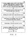
- FIG. 3 is a method for providing a modified Brokaw bandgap circuit in accordance with the disclosure.
- a method of providing a bandgap voltage reference includes a first step providing a first npn bipolar transistor, a second npn bipolar transistor, a third npn bipolar transistor, a first resistor, a second resistor, a third resistor, a fourth resistor, and a first, second and third p-channel MOSFET 230, a second step forming a emitter ratio of 1:M for said first and said second npn bipolar transistors 240, a third step matching said second resistor and said third resistor 250, a fourth step establishing a ⁇ Vbe dependent current from said first and third npn bipolar transistor 260; a fifth step establishing a ⁇ Vbe with said fourth resistor 270, and, a sixth step calculating a bandgap output voltage as a function of of Vbe, ⁇ Vbe, and said first resistor
- the npn bipolar transistors can be a homo-junction bipolar transistor or a hetero-junction bipolar transistors.
- Homo-junction bipolar transistors can be silicon, or gallium.
- Hetero-junction bipolar transistors can be silicon germanium (SiGe), silicon germanium carbon (SiGeC), gallium arsenide (GaAs), or indium phosphide (InP).
- the p-channel MOSFET devices can be power transistors, such as LDMOS transistors.
- a modified Brokaw bandgap circuit with improvement for low voltage power supplies are herein described.
- the improvement is achieved with minimal impact on silicon area or power usage.
- the improved bandgap reference circuit improves temperature insensitivity and operability at low power supply voltages by the addition of a transistor element, and resistor element.
Landscapes
- Engineering & Computer Science (AREA)
- Physics & Mathematics (AREA)
- Electromagnetism (AREA)
- General Physics & Mathematics (AREA)
- Radar, Positioning & Navigation (AREA)
- Automation & Control Theory (AREA)
- Microelectronics & Electronic Packaging (AREA)
- Nonlinear Science (AREA)
- Power Engineering (AREA)
- Control Of Electrical Variables (AREA)
Priority Applications (2)
| Application Number | Priority Date | Filing Date | Title |
|---|---|---|---|
| EP14368016.3A EP2905672A1 (de) | 2014-02-11 | 2014-02-11 | Vorrichtung und Verfahren für eine gewünschte Brokaw-Bandlückenreferenzschaltung für verbesserte Niederspannungsversorgung |
| US14/181,749 US9471084B2 (en) | 2014-02-11 | 2014-02-17 | Apparatus and method for a modified brokaw bandgap reference circuit for improved low voltage power supply |
Applications Claiming Priority (1)
| Application Number | Priority Date | Filing Date | Title |
|---|---|---|---|
| EP14368016.3A EP2905672A1 (de) | 2014-02-11 | 2014-02-11 | Vorrichtung und Verfahren für eine gewünschte Brokaw-Bandlückenreferenzschaltung für verbesserte Niederspannungsversorgung |
Publications (1)
| Publication Number | Publication Date |
|---|---|
| EP2905672A1 true EP2905672A1 (de) | 2015-08-12 |
Family
ID=50239565
Family Applications (1)
| Application Number | Title | Priority Date | Filing Date |
|---|---|---|---|
| EP14368016.3A Withdrawn EP2905672A1 (de) | 2014-02-11 | 2014-02-11 | Vorrichtung und Verfahren für eine gewünschte Brokaw-Bandlückenreferenzschaltung für verbesserte Niederspannungsversorgung |
Country Status (2)
| Country | Link |
|---|---|
| US (1) | US9471084B2 (de) |
| EP (1) | EP2905672A1 (de) |
Cited By (3)
| Publication number | Priority date | Publication date | Assignee | Title |
|---|---|---|---|---|
| CN106855732A (zh) * | 2016-12-26 | 2017-06-16 | 中山大学 | 一种超低功耗基准电压源电路系统 |
| CN112433556A (zh) * | 2019-08-26 | 2021-03-02 | 圣邦微电子(北京)股份有限公司 | 一种改进的带隙基准电压电路 |
| CN114967818A (zh) * | 2022-07-26 | 2022-08-30 | 苏州锴威特半导体股份有限公司 | 一种低温漂偏置的带隙基准电路 |
Families Citing this family (9)
| Publication number | Priority date | Publication date | Assignee | Title |
|---|---|---|---|---|
| US10209732B2 (en) * | 2016-03-16 | 2019-02-19 | Allegro Microsystems, Llc | Bandgap reference circuit with tunable current source |
| US11740281B2 (en) | 2018-01-08 | 2023-08-29 | Proteantecs Ltd. | Integrated circuit degradation estimation and time-of-failure prediction using workload and margin sensing |
| US10331151B1 (en) * | 2018-11-28 | 2019-06-25 | Micron Technology, Inc. | Systems for generating process, voltage, temperature (PVT)-independent current |
| US11271566B2 (en) * | 2018-12-14 | 2022-03-08 | Integrated Device Technology, Inc. | Digital logic compatible inputs in compound semiconductor circuits |
| EP3812873B1 (de) * | 2019-10-24 | 2025-02-26 | NXP USA, Inc. | Spannungsreferenzerzeugung mit kompensation von temperaturschwankungen |
| EP3929694B1 (de) * | 2020-06-22 | 2023-08-30 | NXP USA, Inc. | Spannungsregler |
| RU2767980C1 (ru) * | 2021-07-21 | 2022-03-22 | Павел Юрьевич Иванов | Источник опорного напряжения |
| US11619551B1 (en) * | 2022-01-27 | 2023-04-04 | Proteantecs Ltd. | Thermal sensor for integrated circuit |
| US12399522B2 (en) | 2022-11-25 | 2025-08-26 | Lx Semicon Co., Ltd. | Band gap reference circuit under low supply voltage |
Citations (11)
| Publication number | Priority date | Publication date | Assignee | Title |
|---|---|---|---|---|
| US4789819A (en) * | 1986-11-18 | 1988-12-06 | Linear Technology Corporation | Breakpoint compensation and thermal limit circuit |
| US5982201A (en) | 1998-01-13 | 1999-11-09 | Analog Devices, Inc. | Low voltage current mirror and CTAT current source and method |
| US6407622B1 (en) * | 2001-03-13 | 2002-06-18 | Ion E. Opris | Low-voltage bandgap reference circuit |
| US20040124822A1 (en) * | 2002-12-27 | 2004-07-01 | Stefan Marinca | Bandgap voltage reference circuit with high power supply rejection ratio (PSRR) and curvature correction |
| US6946825B2 (en) | 2002-10-09 | 2005-09-20 | Stmicroelectronics S.A. | Bandgap voltage generator with a bipolar assembly and a mirror assembly |
| US7199646B1 (en) | 2003-09-23 | 2007-04-03 | Cypress Semiconductor Corp. | High PSRR, high accuracy, low power supply bandgap circuit |
| US7208930B1 (en) | 2005-01-10 | 2007-04-24 | Analog Devices, Inc. | Bandgap voltage regulator |
| US20070257729A1 (en) * | 2006-05-02 | 2007-11-08 | Freescale Semiconductor, Inc. | Reference circuit and method for generating a reference signal from a reference circuit |
| US20080088361A1 (en) * | 2006-10-16 | 2008-04-17 | Nec Electronics Corporation | Reference voltage generating circuit |
| US7400187B1 (en) * | 2001-10-02 | 2008-07-15 | National Semiconductor Corporation | Low voltage, low Z, band-gap reference |
| US20100123514A1 (en) * | 2008-11-18 | 2010-05-20 | Microchip Technology Incorporated | Systems and methods for trimming bandgap offset with bipolar diode elements |
Family Cites Families (1)
| Publication number | Priority date | Publication date | Assignee | Title |
|---|---|---|---|---|
| US7714563B2 (en) * | 2007-03-13 | 2010-05-11 | Analog Devices, Inc. | Low noise voltage reference circuit |
-
2014
- 2014-02-11 EP EP14368016.3A patent/EP2905672A1/de not_active Withdrawn
- 2014-02-17 US US14/181,749 patent/US9471084B2/en active Active
Patent Citations (11)
| Publication number | Priority date | Publication date | Assignee | Title |
|---|---|---|---|---|
| US4789819A (en) * | 1986-11-18 | 1988-12-06 | Linear Technology Corporation | Breakpoint compensation and thermal limit circuit |
| US5982201A (en) | 1998-01-13 | 1999-11-09 | Analog Devices, Inc. | Low voltage current mirror and CTAT current source and method |
| US6407622B1 (en) * | 2001-03-13 | 2002-06-18 | Ion E. Opris | Low-voltage bandgap reference circuit |
| US7400187B1 (en) * | 2001-10-02 | 2008-07-15 | National Semiconductor Corporation | Low voltage, low Z, band-gap reference |
| US6946825B2 (en) | 2002-10-09 | 2005-09-20 | Stmicroelectronics S.A. | Bandgap voltage generator with a bipolar assembly and a mirror assembly |
| US20040124822A1 (en) * | 2002-12-27 | 2004-07-01 | Stefan Marinca | Bandgap voltage reference circuit with high power supply rejection ratio (PSRR) and curvature correction |
| US7199646B1 (en) | 2003-09-23 | 2007-04-03 | Cypress Semiconductor Corp. | High PSRR, high accuracy, low power supply bandgap circuit |
| US7208930B1 (en) | 2005-01-10 | 2007-04-24 | Analog Devices, Inc. | Bandgap voltage regulator |
| US20070257729A1 (en) * | 2006-05-02 | 2007-11-08 | Freescale Semiconductor, Inc. | Reference circuit and method for generating a reference signal from a reference circuit |
| US20080088361A1 (en) * | 2006-10-16 | 2008-04-17 | Nec Electronics Corporation | Reference voltage generating circuit |
| US20100123514A1 (en) * | 2008-11-18 | 2010-05-20 | Microchip Technology Incorporated | Systems and methods for trimming bandgap offset with bipolar diode elements |
Cited By (4)
| Publication number | Priority date | Publication date | Assignee | Title |
|---|---|---|---|---|
| CN106855732A (zh) * | 2016-12-26 | 2017-06-16 | 中山大学 | 一种超低功耗基准电压源电路系统 |
| CN106855732B (zh) * | 2016-12-26 | 2018-03-16 | 中山大学 | 一种超低功耗基准电压源电路系统 |
| CN112433556A (zh) * | 2019-08-26 | 2021-03-02 | 圣邦微电子(北京)股份有限公司 | 一种改进的带隙基准电压电路 |
| CN114967818A (zh) * | 2022-07-26 | 2022-08-30 | 苏州锴威特半导体股份有限公司 | 一种低温漂偏置的带隙基准电路 |
Also Published As
| Publication number | Publication date |
|---|---|
| US20150227156A1 (en) | 2015-08-13 |
| US9471084B2 (en) | 2016-10-18 |
Similar Documents
| Publication | Publication Date | Title |
|---|---|---|
| US9471084B2 (en) | Apparatus and method for a modified brokaw bandgap reference circuit for improved low voltage power supply | |
| US6774711B2 (en) | Low power bandgap voltage reference circuit | |
| US7755344B2 (en) | Ultra low-voltage sub-bandgap voltage reference generator | |
| US6987416B2 (en) | Low-voltage curvature-compensated bandgap reference | |
| US10296026B2 (en) | Low noise reference voltage generator and load regulator | |
| CN109976425B (zh) | 一种低温度系数基准源电路 | |
| US7812663B2 (en) | Bandgap voltage reference circuit | |
| US9459647B2 (en) | Bandgap reference circuit and bandgap reference current source with two operational amplifiers for generating zero temperature correlated current | |
| US20050237045A1 (en) | Bandgap reference circuits | |
| US20090302823A1 (en) | Voltage regulator circuit | |
| US8269478B2 (en) | Two-terminal voltage regulator with current-balancing current mirror | |
| US11662761B2 (en) | Reference voltage circuit | |
| US11604486B2 (en) | Voltage regulator | |
| US10379567B2 (en) | Bandgap reference circuitry | |
| CN113805633B (zh) | 基于高准确度齐纳的电压参考电路 | |
| US7944272B2 (en) | Constant current circuit | |
| US9442508B2 (en) | Reference voltage source and method for providing a curvature-compensated reference voltage | |
| US10416702B2 (en) | Bandgap reference circuit, corresponding device and method | |
| US20050093530A1 (en) | Reference voltage generator | |
| US20140009128A1 (en) | Adjustable Shunt Regulator Circuit | |
| US10642304B1 (en) | Low voltage ultra-low power continuous time reverse bandgap reference circuit | |
| US20100102795A1 (en) | Bandgap voltage reference circuit | |
| US20120153997A1 (en) | Circuit for Generating a Reference Voltage Under a Low Power Supply Voltage | |
| US20170060167A1 (en) | Fractional bandgap with low supply voltage and low current | |
| US12306654B2 (en) | Current reference circuit |
Legal Events
| Date | Code | Title | Description |
|---|---|---|---|
| PUAI | Public reference made under article 153(3) epc to a published international application that has entered the european phase |
Free format text: ORIGINAL CODE: 0009012 |
|
| AK | Designated contracting states |
Kind code of ref document: A1 Designated state(s): AL AT BE BG CH CY CZ DE DK EE ES FI FR GB GR HR HU IE IS IT LI LT LU LV MC MK MT NL NO PL PT RO RS SE SI SK SM TR |
|
| AX | Request for extension of the european patent |
Extension state: BA ME |
|
| RAP1 | Party data changed (applicant data changed or rights of an application transferred) |
Owner name: DIALOG SEMICONDUCTOR (UK) LIMITED |
|
| 17P | Request for examination filed |
Effective date: 20160211 |
|
| RBV | Designated contracting states (corrected) |
Designated state(s): AL AT BE BG CH CY CZ DE DK EE ES FI FR GB GR HR HU IE IS IT LI LT LU LV MC MK MT NL NO PL PT RO RS SE SI SK SM TR |
|
| STAA | Information on the status of an ep patent application or granted ep patent |
Free format text: STATUS: THE APPLICATION IS DEEMED TO BE WITHDRAWN |
|
| 18D | Application deemed to be withdrawn |
Effective date: 20190903 |