EP2905901B1 - Procédé et dispositif de détermination d'une capacité et/ou d'une modification de capacité d'un élément de construction capacitif - Google Patents
Procédé et dispositif de détermination d'une capacité et/ou d'une modification de capacité d'un élément de construction capacitif Download PDFInfo
- Publication number
- EP2905901B1 EP2905901B1 EP15153534.1A EP15153534A EP2905901B1 EP 2905901 B1 EP2905901 B1 EP 2905901B1 EP 15153534 A EP15153534 A EP 15153534A EP 2905901 B1 EP2905901 B1 EP 2905901B1
- Authority
- EP
- European Patent Office
- Prior art keywords
- voltage
- signal
- output signal
- capacitance
- output
- Prior art date
- Legal status (The legal status is an assumption and is not a legal conclusion. Google has not performed a legal analysis and makes no representation as to the accuracy of the status listed.)
- Active
Links
Images

Classifications
-
- G—PHYSICS
- G01—MEASURING; TESTING
- G01R—MEASURING ELECTRIC VARIABLES; MEASURING MAGNETIC VARIABLES
- G01R27/00—Arrangements for measuring resistance, reactance, impedance, or electric characteristics derived therefrom
- G01R27/02—Measuring real or complex resistance, reactance, impedance, or other two-pole characteristics derived therefrom, e.g. time constant
- G01R27/26—Measuring inductance or capacitance; Measuring quality factor, e.g. by using the resonance method; Measuring loss factor; Measuring dielectric constants ; Measuring impedance or related variables
- G01R27/2605—Measuring capacitance
-
- G—PHYSICS
- G01—MEASURING; TESTING
- G01M—TESTING STATIC OR DYNAMIC BALANCE OF MACHINES OR STRUCTURES; TESTING OF STRUCTURES OR APPARATUS, NOT OTHERWISE PROVIDED FOR
- G01M17/00—Testing of vehicles
-
- H—ELECTRICITY
- H03—ELECTRONIC CIRCUITRY
- H03K—PULSE TECHNIQUE
- H03K17/00—Electronic switching or gating, i.e. not by contact-making and –breaking
- H03K17/94—Electronic switching or gating, i.e. not by contact-making and –breaking characterised by the way in which the control signals are generated
- H03K17/945—Proximity switches
- H03K17/955—Proximity switches using a capacitive detector
-
- H—ELECTRICITY
- H03—ELECTRONIC CIRCUITRY
- H03K—PULSE TECHNIQUE
- H03K17/00—Electronic switching or gating, i.e. not by contact-making and –breaking
- H03K17/94—Electronic switching or gating, i.e. not by contact-making and –breaking characterised by the way in which the control signals are generated
- H03K17/96—Touch switches
- H03K17/962—Capacitive touch switches
-
- H—ELECTRICITY
- H03—ELECTRONIC CIRCUITRY
- H03K—PULSE TECHNIQUE
- H03K2217/00—Indexing scheme related to electronic switching or gating, i.e. not by contact-making or -breaking covered by H03K17/00
- H03K2217/94—Indexing scheme related to electronic switching or gating, i.e. not by contact-making or -breaking covered by H03K17/00 characterised by the way in which the control signal is generated
- H03K2217/96—Touch switches
- H03K2217/9607—Capacitive touch switches
- H03K2217/96071—Capacitive touch switches characterised by the detection principle
- H03K2217/960715—Rc-timing; e.g. measurement of variation of charge time or discharge time of the sensor
-
- H—ELECTRICITY
- H03—ELECTRONIC CIRCUITRY
- H03K—PULSE TECHNIQUE
- H03K2217/00—Indexing scheme related to electronic switching or gating, i.e. not by contact-making or -breaking covered by H03K17/00
- H03K2217/94—Indexing scheme related to electronic switching or gating, i.e. not by contact-making or -breaking covered by H03K17/00 characterised by the way in which the control signal is generated
- H03K2217/96—Touch switches
- H03K2217/9607—Capacitive touch switches
- H03K2217/96071—Capacitive touch switches characterised by the detection principle
- H03K2217/960725—Charge-transfer
Definitions
- the present invention relates to a circuit arrangement and a method for detecting a capacitance of a capacitive component and / or a change in the capacitance of a capacitive component according to the preambles of claims 1 and 13.
- a generic circuit arrangement is from the DE 10 2006 029 120 A1 known.
- a control unit for controlling a monostable multivibrator is provided, which is connected to the capacitive component, e.g. B. a sensor electrode or an electrode arrangement of response electrode and reference electrode.
- the control unit is connected to a first input of the monostable multivibrator to transmit control signals to the monostable multivibrator, and the capacitive component is connected to a second input of the monostable multivibrator.
- a control signal generates an output signal at an output of the monostable multivibrator, the duration of which depends on the capacitance of the capacitive component.
- Such an output signal is converted into a signal voltage via a conversion device, the course of which is proportional to the duration of the output signal.
- the signal voltage obtained is thus also proportional to the capacitance of the capacitive component or a change in capacitance, so that the signal voltage is used to infer this can.
- the signal voltage is accordingly evaluated by an evaluation unit in order to generate a detection value therefrom which indicates the current capacitance and / or a change in the capacitance of the capacitive component.
- Such a circuit arrangement can be used, for example, for an adjusting device for a closing element of a vehicle which can be actuated by power, for example for an electromotively adjustable tailgate or side door or an electromotively adjustable trunk lid of a motor vehicle.
- the capacitive component is formed here, for example, by a sensor electrode in order to be able to detect an operating event without contact.
- the measurable capacitance changes through a body part of a user in the area of the sensor electrode, so that a user can specifically trigger an operating event through the respective body part, which is detected via the sensor electrode and is intended to lead to an automatic adjustment of the respective closing element.
- An exemplary application here is the use of a sensor electrode in the area of a rear bumper of a motor vehicle in order to use the sensor electrode to recognize a user's foot in the area of the bumper as a "kick" as an operating event and in response to this the tailgate or the Open the trunk lid of the motor vehicle.
- the adjustment of the closing element in the form of the tailgate or the trunk lid can thus be contactless, i. that is, can be controlled by the user without touching the respective closing element.
- a conversion device with a constant current source and an integrator in the form of a capacitor is proposed.
- the switching on and off of the constant current source or its connection to the integrator is controlled via the output signal of the monostable multivibrator.
- the constant current source thus integrates a signal voltage on the integrator, that is to say the integrator is charged in the form of a capacitor.
- the signal voltage that can be measured via the integrator is evaluated by an electronic evaluation unit, in order, for example, to infer an operating event when a threshold value is exceeded and to generate a trigger signal.
- a trigger signal would then, for example, control the adjustment of a locking element of a motor vehicle.
- From the DE 102 58 417 B3 describes a circuit arrangement for detecting and / or determining the nature of a medium with the aid of a capacitive component in the form of a pair of electrodes, in which a composition of a medium into which the two electrodes are immersed is inferred on the basis of the capacitance which can be measured via the two electrodes.
- the two electrodes are for this with a monostable multivibrator in the DE 102 58 417 B3 referred to as a monostable multivibrator, which generates an output signal of a certain duration depending on the capacitance at the electrodes.
- This output signal is passed through a low-pass filter arranged downstream of the monostable multivibrator to subsequently provide a signal voltage which is evaluated by an evaluation unit.
- the content of water in the respective medium can be determined, for example, and different media, such as diesel fuel, biodiesel fuel and water, can be differentiated on the basis of their different dielectric constants.
- Another circuit arrangement for detecting a capacitance of a capacitive component is from the WO 80/02600 known.
- the present invention is therefore based on the object of further improving a generic circuit arrangement and of providing an improved method for detecting a capacitance and / or a capacitance change in a capacitive component.
- an integrator With an operational amplifier and with at least one capacitor connected in parallel to this, a linear signal voltage is generated at the output of the integrator, to which the evaluation unit is connected, which is directly dependent on the output signal of the monostable multivibrator and thus on the capacitance of the capacitive component depends.
- the integrator is consequently designed according to the invention and connected between the output of the monostable multivibrator and the evaluation unit in such a way that an output signal of the monostable multivibrator is applied to an amplifier input of the operational amplifier and leads to a signal voltage which changes linearly with time, the values representing the signal voltage can assume are directly dependent on the output signal and are predetermined by the output signal
- the solution according to the invention is based on the basic idea of directly further processing the output signal of the monostable multivibrator and preferably also specifying the values that the signal voltage can assume via its voltage values.
- a preferred embodiment variant provides that the monostable multivibrator is designed such that its output signal can assume two discrete voltage values.
- the voltage value of the output signal varies between 0V and a positive voltage value, for example 5V, 10V or 15V.
- the level of the signal voltage can be controllable in the circuit arrangement designed according to the invention with an operational amplifier, preferably via an electronic adjusting device that is independent of the output signal, or in a stepless manner or in predefined steps.
- an operational amplifier preferably via an electronic adjusting device that is independent of the output signal, or in a stepless manner or in predefined steps.
- a gain factor specified by the integrator can be set. If required and depending on the intended use, desired sensitivity, response threshold and / or ambient conditions, an amplification factor between the output signal and signal voltage can thus be adjusted and a characteristic curve for the signal voltage to be evaluated can be changed.
- the current fed back to an input of the operational amplifier is changed using an electronic setting device.
- the steepness of a characteristic curve for the signal voltage can be specifically changed in a simple manner, in particular the characteristic curve can be tilted.
- a switchable setting device by means of which a plurality of discrete values for a gain factor are predetermined and can be selected. Different amplification factors can be specified here via different switching states of the setting device.
- a change in the magnitude of the signal voltage in particular a change in a possible maximum value of the signal voltage that is directly dependent on the output signal, and in turn an adaptation of a characteristic curve for the signal voltage takes place by means of a changed amplification factor.
- an adjusting device has at least one switching means in the form of a field effect transistor, preferably at least two field effect transistors, in order to be able to assume different switching states in an electrically controlled manner.
- An output signal can consequently represent two different states and accordingly specify two different voltages at an amplifier input of the operational amplifier, of which one voltage is below and the other voltage is above the reference voltage present at the other amplifier input.
- a capacitor connected in parallel to the operational amplifier which is connected on the one hand to the amplifier input to which the output signal is present and on the other hand is connected to the output of the operational amplifier, generates a linearly rising or falling voltage signal at the output of the operational amplifier, depending on whether the voltage of the output signal is above or below the reference voltage.
- a supply voltage is provided for operating the operational amplifier and that the circuit arrangement has a voltage divider in order to provide a reference voltage that is present at an amplifier input of the operational amplifier as a partial voltage of this supply voltage.
- the supply voltage can thus be applied at one point in the circuit arrangement and not only a supply connection of the operational amplifier can be connected thereto, but also via a voltage divider of one of the amplifier inputs of the operational amplifier.
- a voltage divider is preferably formed by two resistors.
- the integrator of a circuit arrangement according to the invention defined with the operational amplifier is designed to be inverting. Accordingly, the output signal is present at the inverting (negative) amplifier input of the operational amplifier and the reference voltage at the non-inverting (positive) amplifier input.
- a non-inverting integrator which, for example, only results in linear curves for the signal voltage when output signals remain the same, varying between two voltage values, which are reversed to the curves of the signal voltage in the case of an inverting integrator.
- a peak value holding element is connected downstream of the integrator in order to store a maximum voltage value for the signal voltage (for the control signal just given to the monostable multivibrator).
- the held or stored maximum voltage value can then be compared, for example, with a threshold value for the signal voltage stored in the evaluation unit in order to assess whether this threshold value has been exceeded or fallen short of.
- the evaluation unit can, for example, generate a trigger signal in order to signal that the capacitance of the capacitive component is classified as relevant Has fallen below or exceeded the capacity value or a corresponding change in capacity has occurred.
- a trigger signal can indicate, for example, the presence of an operating event for adjusting a closing element on a vehicle.
- the maximum voltage value stored on the peak value holding element can thus be a detection value which indicates the capacitance and / or a change in the capacitance of the capacitive component, so that the peak value holding element here forms part of an (electronic) evaluation unit.
- the signal voltage can of course also be transmitted directly to an electronic evaluation unit.
- the evaluation unit is able, for example, to obtain a detection value or a plurality of detection values on the basis of the signal curve, in particular, for example, on the basis of the duration of a linear rise or fall in the signal voltage until a threshold value or even a number of threshold values are exceeded or not reached.
- a detection value can, for example, indicate to a downstream control device a capacitance of the capacitive component and / or a change in capacitance.
- the detection value can also be a value that is generated by the evaluation unit in order to indicate qualitatively or quantitatively a specific capacitance value and / or a change in capacitance value in the capacitive component.
- the peak hold element which is connected to the output of the integrator, comprises at least one diode and a storage capacitor. It is of course possible that the maximum voltage value held at the peak value holding element is not identical to a maximum value of the signal voltage generated at the output of the integrator. For example, additional resistances can be provided in the circuit arrangement, so that the voltage held on the storage capacitor of the peak value holding element with the aid of the diode is lower than the signal voltage generated at the output of the integrator. However, the voltage applied to the storage capacitor of the peak value holding element is in any case proportional to the signal voltage.
- a further aspect of the present invention is the provision of a circuit arrangement according to the invention in an adjustment device for an adjustable locking element of a vehicle.
- a body opening of a vehicle can be closed via the closing element and the closing element can be automatically adjustable to release the body opening when an operating event is present.
- a locking of the closing element can be actuated in order to release the closing element and to be able to adjust it at all (manually or powered).
- the closing element is a tailgate or a (side) door of a motor vehicle or a trunk lid of a motor vehicle.
- a capacitively operating sensor device with at least one capacitive component, for example in the form of a single sensor electrode or at least one pair of sensor electrodes, the presence of an operating event is recognized on the basis of the capacitance of the component and / or a change in the capacitance of the component.
- the conversion of the output signal is carried out by means of an integrator which has an operational amplifier to whose one amplifier input the output signal is present, and which the output signal of the monostable multivibrator is linear with time changing Converts signal voltage so that the values that the signal voltage can assume are predetermined by the output signal.
- a possibility for controlling the level of the signal voltage and / or for changing a characteristic curve for the signal voltage is provided by means of a switchable setting device, so that, for example, a gain factor specified by the integrator between the output signal and the signal voltage can be set continuously or in predefined steps if necessary and depending on the intended use, desired sensitivity, response threshold and / or ambient conditions, it can be readily adapted in a targeted manner and, if necessary, a characteristic curve for the signal voltage to be evaluated can be changed.
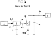
- a control signal is generated by an electronic control unit 1 and transmitted to a monostable multivibrator 2.
- the control unit 1 is connected to a first input 2.1 of the flip-flop 2.
- the monostable multivibrator 2 is connected to a capacitive component 3 at a second input 2.3.
- This capacitive component is shown here in the form of a sensor capacitance 3 and can be, for example, a sensor electrode of a capacitive proximity switch or comprise a sensor capacitor with a response electrode and a reference electrode.
- At least one output signal AS is generated at an output 2.4 of the multivibrator 2 as a result of a control signal from the control unit 1, the duration of which depends on the capacitance or the size of the sensor capacitance 3.
- This output signal AS is used in the circuit arrangement known from the prior art for controlling a switch S in order to connect a constant current source KSQ to an integrator 4 in the form of a capacitor for the duration of the output signal.
- the integrator 4 is charged via the constant current source KSQ, the voltage integrated via the integrator 4 being evaluated as a signal voltage Ss by an electronic evaluation unit 5.
- the signal voltage Ss is proportional to the duration of the output signal AS and is linear over time due to the constant current source KSQ.
- the signal voltage Ss is therefore representative of the size of the sensor capacitance 3 or the capacitance and / or a change in the capacitance of a sensor capacitor formed thereby.
- the evaluation unit 5 can thus form a detection value from the signal voltage Ss, which quantitatively indicates the size of the sensor capacitance 3 and / or which indicates a change in the sensor capacitance 3 qualitatively.
- at least one threshold value is stored, the exceeding or falling below of which causes the generation of a trigger signal by the signal voltage Ss.
- a trigger signal could indicate the presence of an operator event, which is triggered by a power-operated event. that is, in particular via a drive motor, adjustment of a closing element of a vehicle takes place. For example, when a certain operating event sensed by the sensor capacitance 3 is present, an opening or closing of a tailgate or a side door and / or a trunk lid of a motor vehicle can be triggered.
- the constant current source KSQ is switched on and off directly via the trigger signal AS.
- an improved circuit arrangement and an improved method for detecting a capacitance and / or a change in the capacitance of a capacitive component such as the sensor capacitance 3 are provided.
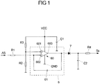
- a conversion device for converting the output signal AS of the monostable multivibrator 2 into a signal voltage Ss for the evaluation unit 5 comprises an inverting integrator 6 with an operational amplifier 60.
- the values that the signal voltage Ss can assume in this circuit arrangement are predetermined directly by the output signal AS.
- the output signal AS is fed via a resistor R1 directly to an inverting (negative) amplifier input 602 of the operational amplifier 60.
- a reference voltage is present at the other non-inverting (positive) amplifier input 601 of the operational amplifier 60, which results as a partial voltage of a supply voltage VCC.
- a voltage divider formed by two series-connected resistors R2 and R3 is provided, through which only a fraction of the supply voltage VCC, for example 1/2 VCC, is present at the non-inverting amplifier input 601.
- the supply voltage VCC specified with respect to ground GND also serves to supply the operational amplifier 60 and is consequently connected to its supply connection.
- a storage capacitor C1 is provided, which is connected to ground GND at the supply voltage VCC. About this optional storage capacitor C1 the operating voltage is stabilized, in particular for the operational amplifier 60.
- a capacitance 61 is connected in parallel to the operational amplifier 60 in a manner known per se and for this purpose is connected both to an output 603 of the operational amplifier 60 and to the inverting amplifier input 602, to which the output signal AS is present.
- the monostable multivibrator 2 is designed here such that an output signal AS with a maximum (constant) voltage value> 0V, for example 5V, is generated as a result of a control signal at its first input 2.1.
- this output signal AS with its maximum value (high level) is applied to the inverting amplifier input 602 for a certain duration.
- the reference voltage at the non-inverting amplifier input 601 is now selected such that it is less than the maximum voltage value of the output signal AS, for example approximately half the maximum value of the output signal AS, for example 2.5V. Accordingly, a signal voltage Ss falling linearly over time is generated at the amplifier output 603, which can drop to 0 V, depending on how long the output signal AS is present with the maximum voltage value.
- the output signal As can also assume a discrete minimum value (low level), the duration of which also depends on the size of the sensor capacitance 3.
- This minimum value is 0V in the present case, so that consequently there is a lower voltage at the inverting amplifier input 602 than at the non-inverting amplifier input 601, at which the constant reference voltage is always present, which is greater than the minimum value of the output signal AS (> 0 V) and at the same time smaller than the maximum value of the output signal AS ( ⁇ 5V).
- V reference 0V ⁇ V reference ⁇ 5V applies here, for example.
- the evaluation unit 5 can thus be used to determine the size of the sensor capacitance 3 and / or a change in the sensor capacitance 3 qualitatively and / or quantitatively.
- the output signal AS with the minimum value of here 0V and the resulting linearly increasing signal voltage Ss is used in order to conclude that a certain operator event is present.
- the presence of a certain operating event is detected when the signal voltage Ss has sufficient time to rise above a threshold value.
- the output signal AS of the monostable multivibrator 2 with the minimum (constant) voltage value of 0V is present here at the operational amplifier 60 so long that the signal voltage Ss generated at the amplifier output 603 increases linearly beyond a response threshold defined by the threshold value, which is considered to be the case of an operator event is evaluated.
- a trigger signal is preferably generated by the evaluation unit 5 in order to open or close a closing element, not shown, such as, for example, a tailgate or a trunk lid of a motor vehicle.
- a change in a capacitance value detected via the sensor capacitance 3, which change is representative of the presence of an operating event, may have been caused, for example, by the proximity of a part of a user's body to the sensor capacitance 3.
- a peak value holding element is provided, which in the present case is formed by a diode 7 and a storage capacitor C2 and a resistor R4 connected in series.
- the storage capacitor C2 is charged by the signal voltage Ss, the diode 7 connected between the amplifier output 603 and the storage capacitor C2 preventing the storage capacitor C2 from being discharged via the operational amplifier 60.
- the storage capacitor C2 is charged in proportion to the signal voltage Ss generated at the amplifier output 603 and maintains a maximum voltage value that has been reached, since discharge by the diode 7 is prevented.
- the signal voltage which can be measured via the storage capacitor C2 thus always represents a maximum value which is representative of the maximum signal voltage Ss reached.
- the voltage held or stored on the storage capacitor C2 can thus be evaluated and compared with at least one threshold value stored in the evaluation unit 5, based on which it is assumed that an operating event has occurred.
- the circuit arrangement of the Figure 1 is supplemented at the output of the operational amplifier 60 by a voltage divider with resistors R5 and R6 and an adjusting device 8 with which variable resistors R7 and R8 can be connected in parallel to the one resistor R6.
- the setting device 8 can thus be used to shift the potential at a node K which lies between the resistors R5 and R6 and to which a line to the capacitance 61 of the integrator 6 and a connecting line 80 of the setting device 8 are connected. In this way, the current fed back to the operational amplifier 60 can be varied depending on which total resistance is connected in series with the resistor R5.
- the setting device 8 can assume several different switching states, in each of which a different total resistance to the resistor R5 is connected in series.
- MOSFET metal oxide semiconductor field effect transistor
- U 81 or U 82 may the be controlled by the respectively assigned resistor R7 or R8 flowing stream, whereby the switched to the resistor R5 in series overall resistance in size is specifically changeable and controllable.
- a maximum value for the signal voltage Ss can be varied in a simple manner, for example increased or decreased between 2.5V and 3.5V, and the slope of the signal voltage Ss can thus be adjusted.
- a switching state of the setting device 8 is not directly dependent on the output signal AS, but is independent and free of it, depending on the need and in particular (current) intended use or ambient conditions of the circuit arrangement.
- the MOSFETs 81 and 82 are in the embodiment of FIG Figure 2 Operated via the control voltages U 81 and U 82 so that the setting device 8 can assume four discrete switching states. In the respective switching state, both, only one or none of the MOSFETs 81 and 82 are activated.
Landscapes
- Physics & Mathematics (AREA)
- General Physics & Mathematics (AREA)
- Measurement Of Resistance Or Impedance (AREA)
- Electronic Switches (AREA)
- Amplifiers (AREA)
Claims (13)
- Ensemble formant circuit servant à détecter une capacité d'un composant capacitif et/ou une modification de la capacité d'un composant capacitif, avec- un circuit bascule (2) monostable pouvant être commandé par un signal de commande avec au moins deux entrées (2.1, 2.3) et une sortie (2.4), dans lequel une première entrée (2.1) du circuit bascule (2) est prévue pour le signal de commande,- un composant (3) capacitif, qui est relié à une deuxième entrée (2.3) du circuit bascule (2) monostable,- un système de conversion, qui est relié à la sortie (2.4) du circuit bascule (2) monostable et est réalisé et prévu pour convertir un signal de sortie (AS) généré au niveau de la sortie (2.4) en une tension de signal (Ss), et- une unité d'évaluation (5), qui est reliée au système de conversion pour évaluer la tension de signal (Ss) et générer sur cette base au moins une valeur de détection, qui indique la capacité et/ou une modification de la capacité du composant (3) capacitif,dans lequel le circuit bascule (2) monostable est réalisé pour générer dans le cas d'un pilotage avec un signal de commande au moins un signal de sortie (AS) au niveau de sa sortie (2.4) dont la durée dépend de la capacité du composant (3) capacitif, et le système de conversion convertit l'au moins un signal de sortie (AS) en une tension de signal (Ss), dont la variation est proportionnelle à la durée du signal de sortie (AS),
dans lequel
le système de conversion comprend un intégrateur (6) avec un amplificateur opérationnel (60) et l'intégrateur (6) est réalisé et branché entre la sortie (2.4) du circuit bascule (2) monostable et l'unité d'évaluation (5) de telle sorte qu'un signal de sortie (AS) du circuit bascule (2) monostable est appliqué au niveau d'une entrée d'amplificateur (602) de l'amplificateur opérationnel (60) et aboutit à une tension de signal (Ss) se modifiant linéairement avec le temps, dans lequel les valeurs, que la tension de signal (Ss) peut adopter, sont spécifiées par le signal de sortie (AS) et dépendent directement du signal de sortie (AS), et
caractérisé en ce que
l'ampleur de la tension de signal (Ss) peut être commandée et/ou une ligne caractéristique pour la tension de signal (Ss) peut être modifiée par l'intermédiaire d'un dispositif de réglage (8) pouvant être commuté, dont l'état de commutation ne dépend pas du signal de sortie (AS) en ce qu'un facteur d'amplification spécifié par l'intégrateur (6) entre le signal de sortie (AS) généré au niveau de la sortie (2.4) du circuit bascule (2) monostable et la tension de signal (Ss) générée par l'intermédiaire du système de conversion peut être réglée par le dispositif de réglage (8). - Ensemble formant circuit selon la revendication 1, caractérisé en ce que plusieurs valeurs discrètes sont spécifiées et peuvent être choisies pour le facteur d'amplification par l'intermédiaire du dispositif de réglage (8) pouvant être commuté.
- Ensemble formant circuit selon la revendication 1 ou 2, caractérisé en ce que le dispositif de réglage (8) est prévu au niveau d'une sortie de l'amplificateur opérationnel (60) et un courant ramené à l'amplificateur opérationnel (60) peut être varié par l'intermédiaire du dispositif de réglage (8) pouvant être commuté.
- Ensemble formant circuit selon l'une quelconque des revendications 1 à 3, caractérisé en ce que le dispositif de réglage (8) présente pour la commande de l'ampleur de la tension de signal (Ss) et/ou d'une modification de la tension de signal (Ss) au moins un transistor à effet de champ (81, 82).
- Ensemble formant circuit selon l'une quelconque des revendications précédentes, caractérisé en ce que le circuit bascule (2) monostable est réalisé de telle manière que son signal de sortie (AS) peut adopter deux valeurs de tension discrètes.
- Ensemble formant circuit selon l'une quelconque des revendications précédentes, caractérisé en ce que le signal de sortie (AS) du circuit bascule (2) monostable- présente une valeur minimale, qui est inférieure à une valeur de tension d'une tension de référence, qui est appliquée au niveau de l'autre entrée d'amplificateur (601) de l'amplificateur opérationnel (60), et- présente une valeur maximale, qui est supérieure à la valeur de tension de la tension de référence sur l'autre entrée d'amplificateur (601).
- Ensemble formant circuit selon l'une quelconque des revendications précédentes, caractérisé en ce que pour faire fonctionner l'amplificateur opérationnel (60), une tension d'alimentation (VCC) est prévue et l'ensemble formant circuit présente un diviseur de tension (R2, R3) pour fournir en tant qu'une tension partielle de la tension d'alimentation (VCC) une tension de référence, qui est appliquée au niveau d'une entrée d'amplificateur (601) de l'amplificateur opérationnel (60).
- Ensemble formant circuit selon l'une quelconque des revendications précédentes, caractérisé en ce que l'intégrateur (6) est inversant.
- Ensemble formant circuit selon l'une quelconque des revendications précédentes, caractérisé en ce qu'un organe de maintien de valeur de pic (7, C2, R4) est branché en aval de l'intégrateur (6) pour mémoriser une valeur de tension maximale de la tension de signal (Ss).
- Ensemble formant circuit selon la revendication 9, caractérisé en ce que l'organe de maintien de valeur de pic (7, C2, R4) comprend au moins une diode (7) et un condensateur accumulateur (C2).
- Ensemble formant circuit selon l'une quelconque des revendications précédentes, caractérisé en ce qu'au moins une valeur de seuil pour la tension de signal (Ss) est enregistrée dans l'unité d'évaluation (5) et l'unité d'évaluation (5) est réalisée pour générer en cas de dépassement ou de valeur inférieure de ladite valeur de seuil par la tension de signal (Ss) un signal de déclenchement.
- Dispositif d'ajustement pour un élément de fermeture ajustable d'un véhicule, dans lequel- une ouverture de carrosserie d'un véhicule peut être fermée par l'intermédiaire de l'élément de fermeture et l'élément de fermeture ajuste automatiquement en présence d'un événement d'utilisateur et/ou un verrouillage de l'élément de fermeture peut être actionné pour dégager l'ouverture de carrosserie, et- un dispositif de capteur à fonctionnement capacitif est prévu avec au moins un composant capacitif pour identifier la présence d'un événement d'utilisateur à l'aide de la capacité du composant et/ou d'une modification de la capacité du composant,caractérisé en ce que
le dispositif d'ajustement servant à détecter la capacité du composant capacitif et/ou une modification de la capacité du composant capacitif comprend un ensemble formant circuit selon l'une quelconque des revendications 1 à 11. - Procédé servant à détecter une capacité d'un composant capacitif et/ou une modification de la capacité d'un composant capacitif, avec des étapes qui suivent :- commande d'un circuit bascule (2) monostable en appliquant un signal de commande sur une première entrée (2.1) du circuit bascule monostable, dans lequel le circuit bascule (2) monostable est relié au niveau d'une deuxième entrée (2.3) au composant (3) capacitif,- génération d'au moins un signal de sortie (AS) au niveau d'une sortie (2.4) du circuit bascule (2) monostable en appliquant le signal de commande, dans lequel la durée du signal de sortie (AS) généré dépend de la capacité du composant (3) capacitif, et- conversion de l'au moins un signal de sortie (AS) en une tension de signal (Ss), dont la variation est proportionnelle à la durée du signal de sortie (AS),dans lequel
la conversion du signal de sortie (AS) est effectuée au moyen de l'intégrateur (6), qui présente un amplificateur opérationnel (60), au niveau d'une entrée d'amplificateur (602) duquel le signal de sortie (AS) est appliqué et qui convertit le signal de sortie (AS) du circuit bascule (2) monostable en une tension de signal (Ss) se modifiant linéairement avec le temps de sorte que les valeurs, que la tension de signal (Ss) peut adopter, sont spécifiées par le signal de sortie (AS) et dépendent directement du signal de sortie (AS), et
caractérisé en ce que
l'ampleur de la tension de signal (Ss) peut être commandée et/ou une courbe caractéristique pour la tension de signal (Ss) peut être modifiée par l'intermédiaire d'un dispositif de réglage (8) pouvant être commuté, dont l'état de commutation ne dépend pas du signal de sortie (AS) en ce qu'un facteur d'amplification spécifié par l'intégrateur (6) entre le signal de sortie (AS) généré au niveau de la sortie (2.4) du circuit bascule (2) monostable et la tension de signal (Ss) générée par l'intermédiaire du système de conversion peut être réglée par le dispositif de réglage (8).
Applications Claiming Priority (2)
| Application Number | Priority Date | Filing Date | Title |
|---|---|---|---|
| DE202014100536.6U DE202014100536U1 (de) | 2014-02-06 | 2014-02-06 | Schaltungsanordnung zur Erfassung einer Kapazität und/oder einer Kapazitätsänderung eines kapazitiven Bauelements |
| DE102014202216.9A DE102014202216A1 (de) | 2014-02-06 | 2014-02-06 | Schaltungsanordnung und Verfahren zur Erfassung einer Kapazität und/oder einer Kapazitätsänderung eines kapazitiven Bauelements |
Publications (2)
| Publication Number | Publication Date |
|---|---|
| EP2905901A1 EP2905901A1 (fr) | 2015-08-12 |
| EP2905901B1 true EP2905901B1 (fr) | 2019-12-18 |
Family
ID=52472183
Family Applications (1)
| Application Number | Title | Priority Date | Filing Date |
|---|---|---|---|
| EP15153534.1A Active EP2905901B1 (fr) | 2014-02-06 | 2015-02-03 | Procédé et dispositif de détermination d'une capacité et/ou d'une modification de capacité d'un élément de construction capacitif |
Country Status (5)
| Country | Link |
|---|---|
| US (1) | US9541590B2 (fr) |
| EP (1) | EP2905901B1 (fr) |
| JP (1) | JP6060340B2 (fr) |
| KR (1) | KR101723914B1 (fr) |
| CN (1) | CN204498082U (fr) |
Families Citing this family (6)
| Publication number | Priority date | Publication date | Assignee | Title |
|---|---|---|---|---|
| DE102011121775B3 (de) | 2011-12-21 | 2013-01-31 | Brose Fahrzeugteile Gmbh & Co. Kg, Hallstadt | Steuersystem |
| DE102015119701A1 (de) * | 2015-11-15 | 2017-05-18 | Brose Fahrzeugteile Gmbh & Co. Kommanditgesellschaft, Bamberg | Verfahren für den Betrieb einer kapazitiven Sensoranordnung eines Kraftfahrzeugs |
| KR102073737B1 (ko) | 2018-12-03 | 2020-02-05 | 송청담 | 고속 정전용량 검출 회로 |
| DE102018131856A1 (de) * | 2018-12-12 | 2020-06-18 | Huf Hülsbeck & Fürst Gmbh & Co. Kg | Anordnung für ein Fahrzeug |
| CN114765021A (zh) * | 2021-01-15 | 2022-07-19 | 晟矽微电子(南京)有限公司 | 驱动装置、驱动芯片及电子设备 |
| US11906559B2 (en) * | 2021-06-24 | 2024-02-20 | Microchip Technology Incorporated | Enhanced impedance measurement using CTMU |
Family Cites Families (8)
| Publication number | Priority date | Publication date | Assignee | Title |
|---|---|---|---|---|
| FR2208121B1 (fr) | 1972-11-29 | 1978-12-29 | Commissariat Energie Atomique | |
| WO1980002600A1 (fr) * | 1979-05-22 | 1980-11-27 | S Dahlqvist | Disposition de detection et de mesure de petites variations de capacitance |
| DE8901346U1 (de) * | 1989-02-07 | 1989-05-24 | Unitronic Elektronische Steuergeräte GmbH, 7530 Pforzheim | Stellvorrichtung für ein elektrisches Steuergerät zum Steuern der Drehzahl von Mikromotoren |
| DE4226137A1 (de) * | 1992-08-07 | 1994-02-10 | Honeywell Regelsysteme Gmbh | Schaltungsanordnung zur Auswertung des Signales eines kapazitiven Meßwertfühlers |
| DE10258417B3 (de) | 2002-12-13 | 2004-08-12 | Beru Ag | Verfahren und Schaltungsanordnung zum Erfassen und/oder Bestimmen der Beschaffenheit eines Mediums |
| DE102006029120B4 (de) | 2006-06-22 | 2014-11-06 | Ifm Electronic Gmbh | Schaltungsanordnung zur Erfassung der Kapazität bzw. einer Kapazitätsänderung eines kapazitiven Schaltungs- oder Bauelements |
| DE102010049400A1 (de) * | 2010-10-26 | 2012-04-26 | Brose Fahrzeugteile Gmbh & Co. Kommanditgesellschaft, Hallstadt | Sensoreinheit zum berührungslosen Betätigen einer Fahrzeugtür |
| KR101202745B1 (ko) * | 2011-04-21 | 2012-11-19 | 주식회사 실리콘웍스 | 터치감지회로 |
-
2015
- 2015-02-03 EP EP15153534.1A patent/EP2905901B1/fr active Active
- 2015-02-04 US US14/614,240 patent/US9541590B2/en active Active
- 2015-02-05 JP JP2015020896A patent/JP6060340B2/ja not_active Expired - Fee Related
- 2015-02-06 CN CN201520087320.5U patent/CN204498082U/zh not_active Expired - Lifetime
- 2015-02-06 KR KR1020150018689A patent/KR101723914B1/ko not_active Expired - Fee Related
Non-Patent Citations (1)
| Title |
|---|
| None * |
Also Published As
| Publication number | Publication date |
|---|---|
| JP6060340B2 (ja) | 2017-01-18 |
| JP2015167351A (ja) | 2015-09-24 |
| EP2905901A1 (fr) | 2015-08-12 |
| KR20150093131A (ko) | 2015-08-17 |
| US9541590B2 (en) | 2017-01-10 |
| CN204498082U (zh) | 2015-07-22 |
| US20150219703A1 (en) | 2015-08-06 |
| KR101723914B1 (ko) | 2017-04-06 |
Similar Documents
| Publication | Publication Date | Title |
|---|---|---|
| EP2905901B1 (fr) | Procédé et dispositif de détermination d'une capacité et/ou d'une modification de capacité d'un élément de construction capacitif | |
| EP3701274A1 (fr) | Procédé pour faire fonctionner un capteur de batterie et capteur de batterie | |
| DE102014216998B4 (de) | Kapazitiver Sensor, die zugehörige Auswerteschaltung und Aktor in einem Kraftfahrzeug | |
| DE102012105266B4 (de) | Kapazitiver Annäherungssensor für ein Kraftfahrzeug | |
| DE102013112909A1 (de) | Kapazitive Sensoreinrichtung mit zugehöriger Auswerteschaltung | |
| DE102011010620A1 (de) | Verfahren zum Messen einer Kapazität | |
| WO2014060330A1 (fr) | Procédé et dispositif de mesure d'un courant circulant dans un interrupteur | |
| EP2550740B1 (fr) | Élément électronique pour un dispositif de capteur, dispositif de capteur et procédé de configuration d'un dispositif de capteur | |
| DE102013013203A1 (de) | Kapazitiver Sensor zur Erfassung von Änderungen um einen Griff | |
| EP3457369B1 (fr) | Circuit pour capteur de fumée | |
| DE102006029120B4 (de) | Schaltungsanordnung zur Erfassung der Kapazität bzw. einer Kapazitätsänderung eines kapazitiven Schaltungs- oder Bauelements | |
| EP3042167A2 (fr) | Dispositif de fonctionnement de capteurs infrarouges passifs | |
| DE102004050691B4 (de) | Antriebsvorrichtung für ein elektrisch betätigtes Fenster | |
| DE102012012865A1 (de) | Kapazitiver Sensor für eine Kollisionsschutzvorrichtung | |
| DE102009047099A1 (de) | Verfahren zum Erfassen eines von einem Sensor mit Stromschnittstelle ausgegebenen ersten Stromsignals | |
| DE102011078694B4 (de) | Verfahren zum Betreiben eines piezokeramischen Sensors und Schaltung zur Durchführung des Verfahrens | |
| DE102004031625A1 (de) | Schaltungsanordnung zur Diagnose eines Heizwiderstands | |
| DE102014202216A1 (de) | Schaltungsanordnung und Verfahren zur Erfassung einer Kapazität und/oder einer Kapazitätsänderung eines kapazitiven Bauelements | |
| EP3667918B1 (fr) | Agencement pour un véhicule | |
| DE202014100536U1 (de) | Schaltungsanordnung zur Erfassung einer Kapazität und/oder einer Kapazitätsänderung eines kapazitiven Bauelements | |
| DE102018113253A1 (de) | Anordnung | |
| EP3257156B1 (fr) | Procédé pour le fonctionnement d'un générateur d'impulsions pour capteurs capacitifs et générateur d'impulsions | |
| EP3457569B1 (fr) | Arrangement d'évaluation pour un dispositif de capteur capacitif | |
| DE102005020870B4 (de) | Sensorschaltung | |
| DE102013222759A1 (de) | Ladungsverstärker für einen kapazitiven Sensor |
Legal Events
| Date | Code | Title | Description |
|---|---|---|---|
| PUAI | Public reference made under article 153(3) epc to a published international application that has entered the european phase |
Free format text: ORIGINAL CODE: 0009012 |
|
| AK | Designated contracting states |
Kind code of ref document: A1 Designated state(s): AL AT BE BG CH CY CZ DE DK EE ES FI FR GB GR HR HU IE IS IT LI LT LU LV MC MK MT NL NO PL PT RO RS SE SI SK SM TR |
|
| AX | Request for extension of the european patent |
Extension state: BA ME |
|
| RIN1 | Information on inventor provided before grant (corrected) |
Inventor name: DAIMINGER, RALF Inventor name: GEUTHER, UDO Inventor name: RUSS, DETLEF |
|
| 17P | Request for examination filed |
Effective date: 20160210 |
|
| RBV | Designated contracting states (corrected) |
Designated state(s): AL AT BE BG CH CY CZ DE DK EE ES FI FR GB GR HR HU IE IS IT LI LT LU LV MC MK MT NL NO PL PT RO RS SE SI SK SM TR |
|
| RAP1 | Party data changed (applicant data changed or rights of an application transferred) |
Owner name: BROSE FAHRZEUGTEILE GMBH & CO. KOMMANDITGESELLSCHA |
|
| GRAP | Despatch of communication of intention to grant a patent |
Free format text: ORIGINAL CODE: EPIDOSNIGR1 |
|
| STAA | Information on the status of an ep patent application or granted ep patent |
Free format text: STATUS: GRANT OF PATENT IS INTENDED |
|
| INTG | Intention to grant announced |
Effective date: 20190819 |
|
| GRAS | Grant fee paid |
Free format text: ORIGINAL CODE: EPIDOSNIGR3 |
|
| GRAA | (expected) grant |
Free format text: ORIGINAL CODE: 0009210 |
|
| STAA | Information on the status of an ep patent application or granted ep patent |
Free format text: STATUS: THE PATENT HAS BEEN GRANTED |
|
| AK | Designated contracting states |
Kind code of ref document: B1 Designated state(s): AL AT BE BG CH CY CZ DE DK EE ES FI FR GB GR HR HU IE IS IT LI LT LU LV MC MK MT NL NO PL PT RO RS SE SI SK SM TR |
|
| REG | Reference to a national code |
Ref country code: CH Ref legal event code: EP |
|
| REG | Reference to a national code |
Ref country code: IE Ref legal event code: FG4D Free format text: LANGUAGE OF EP DOCUMENT: GERMAN |
|
| REG | Reference to a national code |
Ref country code: DE Ref legal event code: R096 Ref document number: 502015011236 Country of ref document: DE |
|
| REG | Reference to a national code |
Ref country code: AT Ref legal event code: REF Ref document number: 1215690 Country of ref document: AT Kind code of ref document: T Effective date: 20200115 |
|
| REG | Reference to a national code |
Ref country code: DE Ref legal event code: R081 Ref document number: 502015011236 Country of ref document: DE Owner name: BROSE FAHRZEUGTEILE SE & CO. KOMMANDITGESELLSC, DE Free format text: FORMER OWNER: BROSE FAHRZEUGTEILE GMBH & CO. KOMMANDITGESELLSCHAFT, BAMBERG, 96052 BAMBERG, DE |
|
| REG | Reference to a national code |
Ref country code: NL Ref legal event code: MP Effective date: 20191218 |
|
| PG25 | Lapsed in a contracting state [announced via postgrant information from national office to epo] |
Ref country code: BG Free format text: LAPSE BECAUSE OF FAILURE TO SUBMIT A TRANSLATION OF THE DESCRIPTION OR TO PAY THE FEE WITHIN THE PRESCRIBED TIME-LIMIT Effective date: 20200318 Ref country code: FI Free format text: LAPSE BECAUSE OF FAILURE TO SUBMIT A TRANSLATION OF THE DESCRIPTION OR TO PAY THE FEE WITHIN THE PRESCRIBED TIME-LIMIT Effective date: 20191218 Ref country code: LV Free format text: LAPSE BECAUSE OF FAILURE TO SUBMIT A TRANSLATION OF THE DESCRIPTION OR TO PAY THE FEE WITHIN THE PRESCRIBED TIME-LIMIT Effective date: 20191218 Ref country code: SE Free format text: LAPSE BECAUSE OF FAILURE TO SUBMIT A TRANSLATION OF THE DESCRIPTION OR TO PAY THE FEE WITHIN THE PRESCRIBED TIME-LIMIT Effective date: 20191218 Ref country code: NO Free format text: LAPSE BECAUSE OF FAILURE TO SUBMIT A TRANSLATION OF THE DESCRIPTION OR TO PAY THE FEE WITHIN THE PRESCRIBED TIME-LIMIT Effective date: 20200318 Ref country code: GR Free format text: LAPSE BECAUSE OF FAILURE TO SUBMIT A TRANSLATION OF THE DESCRIPTION OR TO PAY THE FEE WITHIN THE PRESCRIBED TIME-LIMIT Effective date: 20200319 Ref country code: LT Free format text: LAPSE BECAUSE OF FAILURE TO SUBMIT A TRANSLATION OF THE DESCRIPTION OR TO PAY THE FEE WITHIN THE PRESCRIBED TIME-LIMIT Effective date: 20191218 |
|
| PGFP | Annual fee paid to national office [announced via postgrant information from national office to epo] |
Ref country code: GB Payment date: 20200122 Year of fee payment: 6 |
|
| REG | Reference to a national code |
Ref country code: LT Ref legal event code: MG4D |
|
| PG25 | Lapsed in a contracting state [announced via postgrant information from national office to epo] |
Ref country code: HR Free format text: LAPSE BECAUSE OF FAILURE TO SUBMIT A TRANSLATION OF THE DESCRIPTION OR TO PAY THE FEE WITHIN THE PRESCRIBED TIME-LIMIT Effective date: 20191218 Ref country code: RS Free format text: LAPSE BECAUSE OF FAILURE TO SUBMIT A TRANSLATION OF THE DESCRIPTION OR TO PAY THE FEE WITHIN THE PRESCRIBED TIME-LIMIT Effective date: 20191218 |
|
| PG25 | Lapsed in a contracting state [announced via postgrant information from national office to epo] |
Ref country code: AL Free format text: LAPSE BECAUSE OF FAILURE TO SUBMIT A TRANSLATION OF THE DESCRIPTION OR TO PAY THE FEE WITHIN THE PRESCRIBED TIME-LIMIT Effective date: 20191218 |
|
| PGFP | Annual fee paid to national office [announced via postgrant information from national office to epo] |
Ref country code: FR Payment date: 20200113 Year of fee payment: 6 |
|
| PG25 | Lapsed in a contracting state [announced via postgrant information from national office to epo] |
Ref country code: NL Free format text: LAPSE BECAUSE OF FAILURE TO SUBMIT A TRANSLATION OF THE DESCRIPTION OR TO PAY THE FEE WITHIN THE PRESCRIBED TIME-LIMIT Effective date: 20191218 Ref country code: CZ Free format text: LAPSE BECAUSE OF FAILURE TO SUBMIT A TRANSLATION OF THE DESCRIPTION OR TO PAY THE FEE WITHIN THE PRESCRIBED TIME-LIMIT Effective date: 20191218 Ref country code: PT Free format text: LAPSE BECAUSE OF FAILURE TO SUBMIT A TRANSLATION OF THE DESCRIPTION OR TO PAY THE FEE WITHIN THE PRESCRIBED TIME-LIMIT Effective date: 20200513 Ref country code: RO Free format text: LAPSE BECAUSE OF FAILURE TO SUBMIT A TRANSLATION OF THE DESCRIPTION OR TO PAY THE FEE WITHIN THE PRESCRIBED TIME-LIMIT Effective date: 20191218 Ref country code: EE Free format text: LAPSE BECAUSE OF FAILURE TO SUBMIT A TRANSLATION OF THE DESCRIPTION OR TO PAY THE FEE WITHIN THE PRESCRIBED TIME-LIMIT Effective date: 20191218 |
|
| PG25 | Lapsed in a contracting state [announced via postgrant information from national office to epo] |
Ref country code: SM Free format text: LAPSE BECAUSE OF FAILURE TO SUBMIT A TRANSLATION OF THE DESCRIPTION OR TO PAY THE FEE WITHIN THE PRESCRIBED TIME-LIMIT Effective date: 20191218 Ref country code: SK Free format text: LAPSE BECAUSE OF FAILURE TO SUBMIT A TRANSLATION OF THE DESCRIPTION OR TO PAY THE FEE WITHIN THE PRESCRIBED TIME-LIMIT Effective date: 20191218 Ref country code: IS Free format text: LAPSE BECAUSE OF FAILURE TO SUBMIT A TRANSLATION OF THE DESCRIPTION OR TO PAY THE FEE WITHIN THE PRESCRIBED TIME-LIMIT Effective date: 20200418 |
|
| REG | Reference to a national code |
Ref country code: DE Ref legal event code: R097 Ref document number: 502015011236 Country of ref document: DE |
|
| REG | Reference to a national code |
Ref country code: CH Ref legal event code: PL |
|
| PLBE | No opposition filed within time limit |
Free format text: ORIGINAL CODE: 0009261 |
|
| STAA | Information on the status of an ep patent application or granted ep patent |
Free format text: STATUS: NO OPPOSITION FILED WITHIN TIME LIMIT |
|
| REG | Reference to a national code |
Ref country code: BE Ref legal event code: MM Effective date: 20200229 |
|
| PG25 | Lapsed in a contracting state [announced via postgrant information from national office to epo] |
Ref country code: MC Free format text: LAPSE BECAUSE OF FAILURE TO SUBMIT A TRANSLATION OF THE DESCRIPTION OR TO PAY THE FEE WITHIN THE PRESCRIBED TIME-LIMIT Effective date: 20191218 Ref country code: ES Free format text: LAPSE BECAUSE OF FAILURE TO SUBMIT A TRANSLATION OF THE DESCRIPTION OR TO PAY THE FEE WITHIN THE PRESCRIBED TIME-LIMIT Effective date: 20191218 Ref country code: LU Free format text: LAPSE BECAUSE OF NON-PAYMENT OF DUE FEES Effective date: 20200203 Ref country code: DK Free format text: LAPSE BECAUSE OF FAILURE TO SUBMIT A TRANSLATION OF THE DESCRIPTION OR TO PAY THE FEE WITHIN THE PRESCRIBED TIME-LIMIT Effective date: 20191218 |
|
| 26N | No opposition filed |
Effective date: 20200921 |
|
| PG25 | Lapsed in a contracting state [announced via postgrant information from national office to epo] |
Ref country code: CH Free format text: LAPSE BECAUSE OF NON-PAYMENT OF DUE FEES Effective date: 20200229 Ref country code: SI Free format text: LAPSE BECAUSE OF FAILURE TO SUBMIT A TRANSLATION OF THE DESCRIPTION OR TO PAY THE FEE WITHIN THE PRESCRIBED TIME-LIMIT Effective date: 20191218 Ref country code: LI Free format text: LAPSE BECAUSE OF NON-PAYMENT OF DUE FEES Effective date: 20200229 |
|
| PG25 | Lapsed in a contracting state [announced via postgrant information from national office to epo] |
Ref country code: IT Free format text: LAPSE BECAUSE OF FAILURE TO SUBMIT A TRANSLATION OF THE DESCRIPTION OR TO PAY THE FEE WITHIN THE PRESCRIBED TIME-LIMIT Effective date: 20191218 Ref country code: IE Free format text: LAPSE BECAUSE OF NON-PAYMENT OF DUE FEES Effective date: 20200203 |
|
| PG25 | Lapsed in a contracting state [announced via postgrant information from national office to epo] |
Ref country code: PL Free format text: LAPSE BECAUSE OF FAILURE TO SUBMIT A TRANSLATION OF THE DESCRIPTION OR TO PAY THE FEE WITHIN THE PRESCRIBED TIME-LIMIT Effective date: 20191218 Ref country code: BE Free format text: LAPSE BECAUSE OF NON-PAYMENT OF DUE FEES Effective date: 20200229 |
|
| REG | Reference to a national code |
Ref country code: AT Ref legal event code: MM01 Ref document number: 1215690 Country of ref document: AT Kind code of ref document: T Effective date: 20200203 |
|
| PG25 | Lapsed in a contracting state [announced via postgrant information from national office to epo] |
Ref country code: AT Free format text: LAPSE BECAUSE OF NON-PAYMENT OF DUE FEES Effective date: 20200203 |
|
| GBPC | Gb: european patent ceased through non-payment of renewal fee |
Effective date: 20210203 |
|
| PG25 | Lapsed in a contracting state [announced via postgrant information from national office to epo] |
Ref country code: GB Free format text: LAPSE BECAUSE OF NON-PAYMENT OF DUE FEES Effective date: 20210203 Ref country code: FR Free format text: LAPSE BECAUSE OF NON-PAYMENT OF DUE FEES Effective date: 20210228 |
|
| PG25 | Lapsed in a contracting state [announced via postgrant information from national office to epo] |
Ref country code: TR Free format text: LAPSE BECAUSE OF FAILURE TO SUBMIT A TRANSLATION OF THE DESCRIPTION OR TO PAY THE FEE WITHIN THE PRESCRIBED TIME-LIMIT Effective date: 20191218 Ref country code: MT Free format text: LAPSE BECAUSE OF FAILURE TO SUBMIT A TRANSLATION OF THE DESCRIPTION OR TO PAY THE FEE WITHIN THE PRESCRIBED TIME-LIMIT Effective date: 20191218 Ref country code: CY Free format text: LAPSE BECAUSE OF FAILURE TO SUBMIT A TRANSLATION OF THE DESCRIPTION OR TO PAY THE FEE WITHIN THE PRESCRIBED TIME-LIMIT Effective date: 20191218 |
|
| PG25 | Lapsed in a contracting state [announced via postgrant information from national office to epo] |
Ref country code: MK Free format text: LAPSE BECAUSE OF FAILURE TO SUBMIT A TRANSLATION OF THE DESCRIPTION OR TO PAY THE FEE WITHIN THE PRESCRIBED TIME-LIMIT Effective date: 20191218 |
|
| REG | Reference to a national code |
Ref country code: DE Ref legal event code: R084 Ref document number: 502015011236 Country of ref document: DE |
|
| PGFP | Annual fee paid to national office [announced via postgrant information from national office to epo] |
Ref country code: DE Payment date: 20260228 Year of fee payment: 12 |