EP2907191B1 - Filtre d'absorption de radiofréquence - Google Patents
Filtre d'absorption de radiofréquence Download PDFInfo
- Publication number
- EP2907191B1 EP2907191B1 EP13847868.0A EP13847868A EP2907191B1 EP 2907191 B1 EP2907191 B1 EP 2907191B1 EP 13847868 A EP13847868 A EP 13847868A EP 2907191 B1 EP2907191 B1 EP 2907191B1
- Authority
- EP
- European Patent Office
- Prior art keywords
- resistive material
- conductive pathway
- conductive
- edge
- point
- Prior art date
- Legal status (The legal status is an assumption and is not a legal conclusion. Google has not performed a legal analysis and makes no representation as to the accuracy of the status listed.)
- Active
Links
Images



Classifications
-
- H—ELECTRICITY
- H05—ELECTRIC TECHNIQUES NOT OTHERWISE PROVIDED FOR
- H05K—PRINTED CIRCUITS; CASINGS OR CONSTRUCTIONAL DETAILS OF ELECTRIC APPARATUS; MANUFACTURE OF ASSEMBLAGES OF ELECTRICAL COMPONENTS
- H05K1/00—Printed circuits
- H05K1/16—Printed circuits incorporating printed electric components, e.g. printed resistors, capacitors or inductors
- H05K1/167—Printed circuits incorporating printed electric components, e.g. printed resistors, capacitors or inductors incorporating printed resistors
-
- H—ELECTRICITY
- H05—ELECTRIC TECHNIQUES NOT OTHERWISE PROVIDED FOR
- H05K—PRINTED CIRCUITS; CASINGS OR CONSTRUCTIONAL DETAILS OF ELECTRIC APPARATUS; MANUFACTURE OF ASSEMBLAGES OF ELECTRICAL COMPONENTS
- H05K1/00—Printed circuits
- H05K1/02—Details
- H05K1/0213—Electrical arrangements not otherwise provided for
- H05K1/0216—Reduction of cross-talk, noise or electromagnetic interference
- H05K1/023—Reduction of cross-talk, noise or electromagnetic interference using auxiliary mounted passive components or auxiliary substances
- H05K1/0234—Resistors or by disposing resistive or lossy substances in or near power planes
-
- H—ELECTRICITY
- H05—ELECTRIC TECHNIQUES NOT OTHERWISE PROVIDED FOR
- H05K—PRINTED CIRCUITS; CASINGS OR CONSTRUCTIONAL DETAILS OF ELECTRIC APPARATUS; MANUFACTURE OF ASSEMBLAGES OF ELECTRICAL COMPONENTS
- H05K3/00—Apparatus or processes for manufacturing printed circuits
- H05K3/02—Apparatus or processes for manufacturing printed circuits in which the conductive material is applied to the surface of the insulating support and is thereafter removed from such areas of the surface which are not intended for current conducting or shielding
- H05K3/06—Apparatus or processes for manufacturing printed circuits in which the conductive material is applied to the surface of the insulating support and is thereafter removed from such areas of the surface which are not intended for current conducting or shielding the conductive material being removed chemically or electrolytically, e.g. by photo-etch process
-
- H—ELECTRICITY
- H05—ELECTRIC TECHNIQUES NOT OTHERWISE PROVIDED FOR
- H05K—PRINTED CIRCUITS; CASINGS OR CONSTRUCTIONAL DETAILS OF ELECTRIC APPARATUS; MANUFACTURE OF ASSEMBLAGES OF ELECTRICAL COMPONENTS
- H05K1/00—Printed circuits
- H05K1/02—Details
- H05K1/0213—Electrical arrangements not otherwise provided for
- H05K1/0237—High frequency adaptations
- H05K1/0242—Structural details of individual signal conductors, e.g. related to the skin effect
-
- H—ELECTRICITY
- H05—ELECTRIC TECHNIQUES NOT OTHERWISE PROVIDED FOR
- H05K—PRINTED CIRCUITS; CASINGS OR CONSTRUCTIONAL DETAILS OF ELECTRIC APPARATUS; MANUFACTURE OF ASSEMBLAGES OF ELECTRICAL COMPONENTS
- H05K2201/00—Indexing scheme relating to printed circuits covered by H05K1/00
- H05K2201/03—Conductive materials
- H05K2201/0332—Structure of the conductor
- H05K2201/0364—Conductor shape
- H05K2201/0379—Stacked conductors
-
- H—ELECTRICITY
- H05—ELECTRIC TECHNIQUES NOT OTHERWISE PROVIDED FOR
- H05K—PRINTED CIRCUITS; CASINGS OR CONSTRUCTIONAL DETAILS OF ELECTRIC APPARATUS; MANUFACTURE OF ASSEMBLAGES OF ELECTRICAL COMPONENTS
- H05K2201/00—Indexing scheme relating to printed circuits covered by H05K1/00
- H05K2201/09—Shape and layout
- H05K2201/09209—Shape and layout details of conductors
- H05K2201/09218—Conductive traces
- H05K2201/09263—Meander
-
- H—ELECTRICITY
- H05—ELECTRIC TECHNIQUES NOT OTHERWISE PROVIDED FOR
- H05K—PRINTED CIRCUITS; CASINGS OR CONSTRUCTIONAL DETAILS OF ELECTRIC APPARATUS; MANUFACTURE OF ASSEMBLAGES OF ELECTRICAL COMPONENTS
- H05K2201/00—Indexing scheme relating to printed circuits covered by H05K1/00
- H05K2201/09—Shape and layout
- H05K2201/09209—Shape and layout details of conductors
- H05K2201/09654—Shape and layout details of conductors covering at least two types of conductors provided for in H05K2201/09218 - H05K2201/095
- H05K2201/09727—Varying width along a single conductor; Conductors or pads having different widths
-
- H—ELECTRICITY
- H05—ELECTRIC TECHNIQUES NOT OTHERWISE PROVIDED FOR
- H05K—PRINTED CIRCUITS; CASINGS OR CONSTRUCTIONAL DETAILS OF ELECTRIC APPARATUS; MANUFACTURE OF ASSEMBLAGES OF ELECTRICAL COMPONENTS
- H05K2201/00—Indexing scheme relating to printed circuits covered by H05K1/00
- H05K2201/09—Shape and layout
- H05K2201/09209—Shape and layout details of conductors
- H05K2201/09654—Shape and layout details of conductors covering at least two types of conductors provided for in H05K2201/09218 - H05K2201/095
- H05K2201/09781—Dummy conductors, i.e. not used for normal transport of current; Dummy electrodes of components
Definitions
- the present disclosure relates generally to a filter configured to absorb radiofrequency (RF) emissions and microwave emissions in particular.
- RF radiofrequency
- Printed circuit boards are structures used to mechanically support and electrically connect electronic components using conductive pathways, tracks, or signal traces etched from sheets of a conductive material laminated onto a non-conductive substrate.
- a circuit board may be required to conduct different types of electrical signals such as microwave or millimeter-wave signals in addition to direct current (DC) or longer wave length signals.
- DC direct current
- the shorter wavelength signals can emit radio-frequency radiation that interferes with the DC or longer wavelength signals rendering operation of the circuit board as problematic.
- new circuit board techniques were developed that would limit or eliminate interference from microwave signals that affect other signals.
- US Patent 5,039,961 discloses a resistive film attenuator element comprised of a dielectric-mounted resistive film distributed ladder network having tuning stubs, combined in a coplanar structure, to provide a wide band attenuator having a substantially flat frequency response over a wide range of frequencies.
- JP Patent 2002 185218 A discloses a microstrip line structure which is capable of reducing EMI where the microstrip line is formed on the surface of a dielectric whose backside is all covered with a conductor and where a resistive layer is provided between the surface of the dielectric and the microstrip line.
- the present invention provides an apparatus and mehod for conveying an electrical signal, as recited in the claims.
- the method includes: etching a conductive material layer to form a conductive pathway configured to convey the electrical signal, the conductive pathway having a first edge and a second edge; and etching a resistive material layer to form a desired shape of a resistive material contacting at least a portion of the conductive pathway, covering an edge of the conductive pathway, and extending beyond the edge, the resistive material having a conductivity less than the conductivity of the conductive material.
- FIG. 1 presents a three-dimensional view of circuit board 2 not forming part of the invention that is configured to transmit or convey an electrical signal 3 from a first point 4 to a second point 5.
- the electrical signal is conveyed through a pathway 6 of a conductive material 7.
- the electrical signal 3 includes a radio-frequency (RF) signal, such as a microwave signal, that can emit RF radiation when the signal is conveyed and a direct-current (DC) or low-frequency signal.
- RF radio-frequency
- DC direct-current
- microwave signal relates to a signal having a wavelength in a range extending from about one (1) millimeter (mm) to about one (1) meter (mm), which is equivalent to a frequency of about 0.3 GHz to about 300 GHz, however, the disclosure herein may also relate to signals extending beyond this range.
- An absorptive filter 10 is disposed on the circuit board 2. The absorptive filter 10 is configured to absorb the RF radiation emitted while the RF signal is being transmitted.
- the absorptive filter 10 includes a resistive material 9 that is in contact with the pathway 6 of the conductive material 7 and overlaps (i.e., covers and extends beyond) the two edges or sides (i.e., first edge 11 and second edge 12) of the pathway 6 as the pathway 6 extends from the first point 4 to the second point 5.
- the RF signal travels along the pathway 6, the magnitude of the current density is highest along the outside edges of the pathway 6, which contrasts with the DC signal current that is distributed evenly throughout the pathway 6.
- the RF radiation is attenuated by being absorbed by the resistive material 9.
- the RF radiation induces currents in the resistive material 9 and the energy of the currents is dissipated as heat by the resistance of the resistive material 9.
- the DC or low frequency signal that travels along the same pathway 6 is not affected by the RF radiation.
- the resistive material 9 is disposed on a dielectric substrate 13 with the conductive material 7 being disposed on the resistive material 9.
- the conductive material 7 that conveys the electrical signal 3 is a highly conductive (i.e., low loss) metal such as copper, silver or gold as non-limiting embodiments.
- the resistive material 9, which dissipates RF induced currents as heat due to the resistivity of the resistive material 9, has a conductivity that is less than the conductivity of the conductive material 9 (or resistivity that is greater than the resistivity of the conductive material 7).
- the resistive material 9 is fabricated to have a desired shape for use in the absorptive filter 10 from a resistive layer or sheet such as a resistive metal having a predetermined sheet resistivity in a range of 25 to 100 ohms per square ( ⁇ / ⁇ ) as a non-limiting embodiment.
- FIG. 2 illustrates a top-view of various absorptive filters 10 whereby the filters with references 27 and 29 do not form part of the present invention and the filter with reference 28 is an embodiment of the present invention.
- a first conductive pathway 21 is configured to convey a DC or low-frequency signal 20.
- a second conductive pathway 22, a third conductive pathway 23 and a fourth conductive pathway 24 are configured to transmit an RF signal 25.
- the resistive material is placed in contact with the second pathway 22 so that the resistive material 9 overlaps the two side-edges 14 and 15.
- the conductive pathway 22 and the resistive material 9 are disposed linearly from point 18 to point 19.
- the resistive material 10 is disposed in a series of stubs or segments 17 where each segment 17 is separated from adjacent segments 17. In addition, each segment 17 overlaps the edges 14 and 15.
- the conductive pathway 24 meanders from point 16 to point 26. The meandering creates differential nodes A, B, C and D. A higher potential (phase difference) created between corresponding nodes causes the RF radiation to dissipate in the resistive material 9 for example from node A to node B and/or from node C to node D.
- the term "meander” relates to a conductive pathway not following a straight path from a signal entry point to a signal exit point.
- a meandering conductive pathway has square, rectangular or curved oscillations about a direction or line from the signal entry point to the signal exit point. It can be appreciated that RF radiation emitted by the RF signal 25 from conductive pathways 22, 23 and 24 will be absorbed by the corresponding absorptive filters 10 and, thus, prevent or limit interference with the DC or low-frequency signal 20 conveyed by the first conductive pathway 21. In alternative embodiments, the DC or low-frequency signal 20 may be conveyed by the conductive pathways 22, 23 or 24 and any RF signals induced on those pathways will be absorbed by the corresponding absorptive filters 10 to prevent or limit interference with the signal 20.
- FIG. 3 illustrates a top-view of an embodiment of the absorptive filter 10.
- separate pieces of the resistive material 9 are disposed over edges 31 and 32 of a conductive pathway 30.
- Extending laterally from each piece of the resistive material 9 or from the pathway 30 are a plurality of resistive stub elements 33 or stubs made of the resistive material 9.
- the resistive stub elements 33 are periodically positioned such that each stub has a corresponding stub positioned oppositely on the other piece of the resistive material 9.
- the resistive stub elements 33 are shaped as a fan as illustrated in FIG. 3 , however, the resistive stub elements 33 may also have other shapes extending from the resistive material 9.
- FIG. 4 illustrates a top-view of another embodiment of the absorptive filter 10.
- the embodiment of FIG. 4 is similar to the embodiment of FIG. 3 with one difference being that the conductive pathway 30 meanders from the first point 41 to the second point 42.
- the resistive material 9 is one-piece and overlaps all edges of the meandering conductive pathway 30.
- the conductive pathway 30 may be straight with a constant width and a path of the resistive material 9 may meander such that the resistive material 9 covers the edges 31 and 32 of the conductive pathway 30.
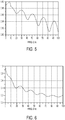
- FIGS. 6 and 7 show that the amount of RF radiation emitted is reduced as much as 80% or more due to the absorptive filter 10.
- the vertical axis in each of FIGS. 5-7 represents an efficiency of absorption of RF power that is transmitted or reflected where a value of 1 represents no loss.
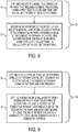
- FIG. 8 is a flow chart for a method 80 for conveying an electrical signal.
- Block 81 calls for applying the electrical signal to a conductive pathway that includes a conductive material, having a first edge and a second edge, and configured to convey the electrical signal.
- Block 82 calls for absorbing radio-frequency radiation using a resistive material contacting at least a portion of the conductive pathway, covering an edge of the conductive pathway, and extending beyond the edge, the resistive material having a conductivity less than the conductivity of the conductive material.
- the method 80 can also include using the various embodiments of the absorptive filter 10 discussed above (including the meandering of the conductive pathway) to absorb the radio-frequency radiation.
- FIG. 9 is a flow chart of a method 90 for fabricating an apparatus for conveying an electrical signal.
- Block 91 calls for etching a conductive material layer to form a conductive pathway configured to convey the electrical signal, the conductive pathway having a first edge and a second edge.
- Block 92 calls for etching a resistive material layer to form a desired shape of a resistive material in contact with at least a portion of the conductive pathway, covering an edge of the conductive pathway, and extending beyond the edge, the resistive material having a conductivity less than the conductivity of the conductive material.
- the method 90 can also include etching the conductive material layer and the resistive material layer to fabricate the various embodiments of the absorptive filter discussed above (including the meandering of the conductive pathway).
- the conductive material 7 and the resistive material 9 can be provided as "raw" or unprocessed embedded layers in the circuit board 2.
- the conductive pathway can be etched to a desired shape (including the meandering conductive pathway) from the layer of the conductive material 7 using techniques for fabrication of semiconductor circuits and components.
- elements of the absorptive filter 10 using the resistive material 9 can be etched to a desired shape (including the resistive stub elements) from the layer of resistive material 9.
- the resistive material may also be etched between two conductive pads to form a resistor having a desired resistance value. It can be further appreciated that these fabrication techniques may provide a cost-effective way of producing microwave circuits on a circuit board where microwave signals may not interfere with DC or low-frequency signals also present on the circuit board.
- a conductive pathway may convey a DC signal to an active electronic device such as a transistor in order to provide a bias to that device.
- the absorptive filter may be applied to the conductive pathway (including meandering of the pathway) in order to absorb and dissipate any RF radiation or energy that may interfere with the DC bias voltage and current.
- the absorptive filter is this case prevents erratic operation or malfunction of the active electronic device.
- a conductive pathway and the absorptive filter can be configured to provide a quarter wave matching structure for impedance matching with a transistor or other electronic device.
- there is no DC signal loss because the DC signal travels along the conductive pathway, which is the lowest resistive path, while RF radiation that travels along the edges of the conductive pathway is dissipated by the resistive material in the absorptive filter.
Landscapes
- Engineering & Computer Science (AREA)
- Microelectronics & Electronic Packaging (AREA)
- Physics & Mathematics (AREA)
- Electromagnetism (AREA)
- Manufacturing & Machinery (AREA)
- Shielding Devices Or Components To Electric Or Magnetic Fields (AREA)
- Manufacturing Cores, Coils, And Magnets (AREA)
- Coils Or Transformers For Communication (AREA)
- Non-Reversible Transmitting Devices (AREA)
- Filters And Equalizers (AREA)
Claims (10)
- Appareil (10) permettant de transporter un signal électrique, l'appareil comprenant :un trajet conducteur (30) comprenant un matériau conducteur, ayant un premier bord (31) et un second bord (32), et configuré pour transporter le signal électrique ; etun matériau résistif (9) en contact avec au moins une partie du trajet conducteur (30), couvrant lesdits bords du trajet conducteur (30), et s'étendant au-delà desdits bords,le matériau résistif (9) ayant une conductivité inférieure à la conductivité du matériau conducteur (30), dans lequellesdits bords comprennent le premier bord (31) au niveau d'un premier côté du trajet conducteur (30) et le second bord (32) au niveau d'un second côté du trajet conducteur (30), dans lequel le matériau résistif (9) s'étend depuis au-delà du premier bord (31) vers au-delà du second bord (32),caractérisé en ce que :
le matériau résistif (9) comprend une pluralité de tronçons (33) du matériau résistif (9) s'étendant latéralement depuis le trajet conducteur (30). - Appareil (10) selon la revendication 1, dans lequel le matériau conducteur (30) ou le matériau résistif (9) est disposé sur un substrat diélectrique (13).
- Appareil (10) selon la revendication 1, dans lequel le signal électrique comprend une composante micro-ondes.
- Appareil (10) selon la revendication 1, dans lequel le matériau résistif (9) comprend une série de segments (17), chaque segment (17) étant séparé d'un segment (17) adjacent.
- Appareil (10) selon la revendication 1, dans lequel le trajet conducteur (30) est configuré pour transporter le signal électrique d'un premier point (4) à un second point (5) et le trajet conducteur serpente du premier point (4) au second point (5).
- Appareil (10) selon la revendication 5, dans lequel le matériau résistif (9) s'étend linéairement du premier point (4) au second point (5).
- Appareil (10) selon la revendication 1, dans lequel le matériau résistif (9) est un métal résistif ayant une surface plane et une valeur de résistivité de couche dans la plage de 25 à 100 ohms par carré.
- Procédé permettant de transporter un signal électrique, le procédé comprenant :l'application du signal électrique à un trajet conducteur (30) comprenant un matériau conducteur, ayant un premier bord (11) et un second bord (12), et configuré pour transporter le signal électrique ; etl'absorption d'un rayonnement radiofréquence à l'aide d'un matériau résistif (9) entrant en contact avec au moins une partie du trajet conducteur (30), couvrant lesdits bords du trajet conducteur (30), et s'étendant au-delà desdits bords, le matériau résistif (9) ayant une conductivité inférieure à la conductivité du matériau conducteur,dans lequel lesdits bords comprennent un premier bord au niveau d'un premier côté du trajet conducteur (30) et un second bord au niveau d'un second côté du trajet conducteur (30), dans lequel le matériau résistif (9) s'étend depuis au-delà du premier bord vers au-delà du second bord,caractérisé en ce que :
le matériau résistif (9) comprend une pluralité de tronçons (33) du matériau résistif (9) s'étendant latéralement depuis le trajet conducteur (30). - Procédé selon la revendication 8, dans lequel le matériau résistif (9) comprend une série de segments (17), chaque segment (17) étant séparé d'un segment adjacent (17) .
- Procédé selon la revendication 8, dans lequel le trajet conducteur (30) est configuré pour transporter le signal électrique d'un premier point à un second point et le trajet conducteur (30) serpente du premier point au second point.
Applications Claiming Priority (2)
| Application Number | Priority Date | Filing Date | Title |
|---|---|---|---|
| US13/651,789 US9078371B2 (en) | 2012-10-15 | 2012-10-15 | Radiofrequency absorptive filter |
| PCT/US2013/054069 WO2014062280A1 (fr) | 2012-10-15 | 2013-08-08 | Filtre d'absorption de radiofréquence |
Publications (3)
| Publication Number | Publication Date |
|---|---|
| EP2907191A1 EP2907191A1 (fr) | 2015-08-19 |
| EP2907191A4 EP2907191A4 (fr) | 2016-04-13 |
| EP2907191B1 true EP2907191B1 (fr) | 2021-03-17 |
Family
ID=50474368
Family Applications (1)
| Application Number | Title | Priority Date | Filing Date |
|---|---|---|---|
| EP13847868.0A Active EP2907191B1 (fr) | 2012-10-15 | 2013-08-08 | Filtre d'absorption de radiofréquence |
Country Status (4)
| Country | Link |
|---|---|
| US (1) | US9078371B2 (fr) |
| EP (1) | EP2907191B1 (fr) |
| JP (1) | JP6351602B2 (fr) |
| WO (1) | WO2014062280A1 (fr) |
Families Citing this family (4)
| Publication number | Priority date | Publication date | Assignee | Title |
|---|---|---|---|---|
| US20170245361A1 (en) * | 2016-01-06 | 2017-08-24 | Nokomis, Inc. | Electronic device and methods to customize electronic device electromagnetic emissions |
| WO2017122269A1 (fr) * | 2016-01-12 | 2017-07-20 | 三菱電機株式会社 | Terminateur et circuit à haute fréquence |
| WO2018122920A1 (fr) * | 2016-12-26 | 2018-07-05 | 三菱電機株式会社 | Dispositif de borne |
| US11509060B2 (en) | 2019-10-21 | 2022-11-22 | City University Of Hong Kong | Filter-antenna and method for making the same |
Citations (1)
| Publication number | Priority date | Publication date | Assignee | Title |
|---|---|---|---|---|
| JP2002185218A (ja) * | 2000-12-15 | 2002-06-28 | Nippon Avionics Co Ltd | マイクロストリップライン |
Family Cites Families (18)
| Publication number | Priority date | Publication date | Assignee | Title |
|---|---|---|---|---|
| JPS60144302U (ja) * | 1984-03-05 | 1985-09-25 | 島田理化工業株式会社 | ストリツプ形減衰素子 |
| US4777718A (en) | 1986-06-30 | 1988-10-18 | Motorola, Inc. | Method of forming and connecting a resistive layer on a pc board |
| US5039961A (en) | 1989-12-21 | 1991-08-13 | Hewlett-Packard Company | Coplanar attenuator element having tuning stubs |
| US6225570B1 (en) * | 1996-12-17 | 2001-05-01 | Kokuriku Electric Industry Co., Ltd. | Circuit board having electric component and its manufacturing method |
| KR100362803B1 (ko) * | 1997-10-02 | 2002-11-29 | 미쓰비시덴키 가부시키가이샤 | 전압 조정 장치 |
| JP3527410B2 (ja) * | 1998-06-15 | 2004-05-17 | 株式会社リコー | コプレーナーストリップライン |
| US6278186B1 (en) | 1998-08-26 | 2001-08-21 | Intersil Corporation | Parasitic current barriers |
| DE29915678U1 (de) * | 1999-09-06 | 2000-10-12 | Siemens AG, 80333 München | Leiterplatte |
| CN1326286C (zh) | 2002-08-01 | 2007-07-11 | 松下电器产业株式会社 | 传送线路和半导体集成电路装置 |
| AU2003271534A1 (en) * | 2002-09-19 | 2004-04-19 | Ilfa Industrieelektronik Und Leiterplattenfertigu Ng Aller Art Gmbh | Hf-reactor |
| US7288723B2 (en) * | 2003-04-02 | 2007-10-30 | Sun Microsystems, Inc. | Circuit board including isolated signal transmission channels |
| WO2005006494A1 (fr) | 2003-06-11 | 2005-01-20 | Bae Systems Information And Electronic Systems Integration Inc. | Procede et appareil permettant de limiter les variations de tension des rapports d'ondes stationnaires vswr dans un ensemble antenne chargee a ligne en meandre large bande compacte |
| US20050260338A1 (en) * | 2004-05-19 | 2005-11-24 | Trendon Touch Technology Corp. | Method of manufacturing circuit layout on touch panel by utilizing metal plating technology |
| US7022464B2 (en) * | 2004-08-25 | 2006-04-04 | Peter Kukanskis | Integral plated resistor and method for the manufacture of printed circuit boards comprising the same |
| JP2007267229A (ja) | 2006-03-29 | 2007-10-11 | Toshiba Corp | マイクロストリップ伝送線路 |
| KR100980678B1 (ko) * | 2008-10-15 | 2010-09-07 | 한국과학기술원 | 위상 천이기 |
| JP5390716B2 (ja) * | 2010-02-15 | 2014-01-15 | モレックス インコーポレイテド | 共振を減少させる回路基板 |
| KR20130126997A (ko) * | 2011-03-01 | 2013-11-21 | 제이엑스 닛코 닛세키 킨조쿠 가부시키가이샤 | 액정 폴리머 필름 베이스 구리 피복 적층판 및 그 제조 방법 |
-
2012
- 2012-10-15 US US13/651,789 patent/US9078371B2/en active Active
-
2013
- 2013-08-08 JP JP2015536767A patent/JP6351602B2/ja active Active
- 2013-08-08 EP EP13847868.0A patent/EP2907191B1/fr active Active
- 2013-08-08 WO PCT/US2013/054069 patent/WO2014062280A1/fr not_active Ceased
Patent Citations (1)
| Publication number | Priority date | Publication date | Assignee | Title |
|---|---|---|---|---|
| JP2002185218A (ja) * | 2000-12-15 | 2002-06-28 | Nippon Avionics Co Ltd | マイクロストリップライン |
Also Published As
| Publication number | Publication date |
|---|---|
| WO2014062280A1 (fr) | 2014-04-24 |
| EP2907191A1 (fr) | 2015-08-19 |
| JP2016504779A (ja) | 2016-02-12 |
| JP6351602B2 (ja) | 2018-07-04 |
| US9078371B2 (en) | 2015-07-07 |
| EP2907191A4 (fr) | 2016-04-13 |
| US20140102774A1 (en) | 2014-04-17 |
Similar Documents
| Publication | Publication Date | Title |
|---|---|---|
| KR101405068B1 (ko) | 고주파 신호 선로 | |
| US5334800A (en) | Flexible shielded circuit board | |
| US8248183B2 (en) | Circuit board pad having impedance matched to a transmission line and method for providing same | |
| CN103748741B (zh) | 天线和电子装置 | |
| TWI778189B (zh) | 高頻傳輸用印刷線路板 | |
| US20150029068A1 (en) | Antenna device | |
| CN115088393B (zh) | 印刷电路板上的导电迹线的弯曲部补偿 | |
| JP6187606B2 (ja) | プリント基板 | |
| EP2907191B1 (fr) | Filtre d'absorption de radiofréquence | |
| KR101560476B1 (ko) | 전자 회로 및 전자 기기 | |
| US20130306363A1 (en) | Structure | |
| US9219299B2 (en) | Resonator, multilayer board and electronic device | |
| JP5176736B2 (ja) | プリント配線基板 | |
| EP2454781A1 (fr) | Filtre hyperfréquence | |
| CN116073119A (zh) | 天线装置 | |
| CN106058442B (zh) | 一种天线 | |
| US20140043190A1 (en) | Planar inverted f antenna structure | |
| JP6282944B2 (ja) | 配線基板およびこれを用いた高周波装置 | |
| JP5082250B2 (ja) | 高周波回路基板 | |
| JP6313124B2 (ja) | 配線基板 | |
| US8994490B2 (en) | Chip resistor with outrigger heat sink | |
| US10321556B2 (en) | Air dielectric printed circuit board | |
| WO2016149269A1 (fr) | Stratégie de mise en page complète de connexion par puce retournée de circuits intégrés | |
| WO2014198998A1 (fr) | Appareil de blindage et procédé de fabrication d'un appareil de blindage | |
| JP2002185091A (ja) | 回路基板、回路基板のemi低減方法およびその回路基板を用いた電子装置のemi低減方法 |
Legal Events
| Date | Code | Title | Description |
|---|---|---|---|
| PUAI | Public reference made under article 153(3) epc to a published international application that has entered the european phase |
Free format text: ORIGINAL CODE: 0009012 |
|
| 17P | Request for examination filed |
Effective date: 20150430 |
|
| AK | Designated contracting states |
Kind code of ref document: A1 Designated state(s): AL AT BE BG CH CY CZ DE DK EE ES FI FR GB GR HR HU IE IS IT LI LT LU LV MC MK MT NL NO PL PT RO RS SE SI SK SM TR |
|
| AX | Request for extension of the european patent |
Extension state: BA ME |
|
| DAX | Request for extension of the european patent (deleted) | ||
| RA4 | Supplementary search report drawn up and despatched (corrected) |
Effective date: 20160315 |
|
| RIC1 | Information provided on ipc code assigned before grant |
Ipc: H01P 1/162 20060101AFI20160309BHEP |
|
| STAA | Information on the status of an ep patent application or granted ep patent |
Free format text: STATUS: EXAMINATION IS IN PROGRESS |
|
| 17Q | First examination report despatched |
Effective date: 20191203 |
|
| REG | Reference to a national code |
Ref country code: DE Ref legal event code: R079 Ref document number: 602013076357 Country of ref document: DE Free format text: PREVIOUS MAIN CLASS: H01P0001162000 Ipc: H05K0001020000 |
|
| GRAP | Despatch of communication of intention to grant a patent |
Free format text: ORIGINAL CODE: EPIDOSNIGR1 |
|
| STAA | Information on the status of an ep patent application or granted ep patent |
Free format text: STATUS: GRANT OF PATENT IS INTENDED |
|
| RIC1 | Information provided on ipc code assigned before grant |
Ipc: H05K 1/02 20060101AFI20201026BHEP |
|
| INTG | Intention to grant announced |
Effective date: 20201123 |
|
| GRAS | Grant fee paid |
Free format text: ORIGINAL CODE: EPIDOSNIGR3 |
|
| GRAA | (expected) grant |
Free format text: ORIGINAL CODE: 0009210 |
|
| STAA | Information on the status of an ep patent application or granted ep patent |
Free format text: STATUS: THE PATENT HAS BEEN GRANTED |
|
| AK | Designated contracting states |
Kind code of ref document: B1 Designated state(s): AL AT BE BG CH CY CZ DE DK EE ES FI FR GB GR HR HU IE IS IT LI LT LU LV MC MK MT NL NO PL PT RO RS SE SI SK SM TR |
|
| REG | Reference to a national code |
Ref country code: GB Ref legal event code: FG4D |
|
| REG | Reference to a national code |
Ref country code: CH Ref legal event code: EP |
|
| REG | Reference to a national code |
Ref country code: DE Ref legal event code: R096 Ref document number: 602013076357 Country of ref document: DE |
|
| REG | Reference to a national code |
Ref country code: IE Ref legal event code: FG4D |
|
| REG | Reference to a national code |
Ref country code: AT Ref legal event code: REF Ref document number: 1373512 Country of ref document: AT Kind code of ref document: T Effective date: 20210415 |
|
| REG | Reference to a national code |
Ref country code: LT Ref legal event code: MG9D |
|
| PG25 | Lapsed in a contracting state [announced via postgrant information from national office to epo] |
Ref country code: HR Free format text: LAPSE BECAUSE OF FAILURE TO SUBMIT A TRANSLATION OF THE DESCRIPTION OR TO PAY THE FEE WITHIN THE PRESCRIBED TIME-LIMIT Effective date: 20210317 Ref country code: FI Free format text: LAPSE BECAUSE OF FAILURE TO SUBMIT A TRANSLATION OF THE DESCRIPTION OR TO PAY THE FEE WITHIN THE PRESCRIBED TIME-LIMIT Effective date: 20210317 Ref country code: GR Free format text: LAPSE BECAUSE OF FAILURE TO SUBMIT A TRANSLATION OF THE DESCRIPTION OR TO PAY THE FEE WITHIN THE PRESCRIBED TIME-LIMIT Effective date: 20210618 Ref country code: NO Free format text: LAPSE BECAUSE OF FAILURE TO SUBMIT A TRANSLATION OF THE DESCRIPTION OR TO PAY THE FEE WITHIN THE PRESCRIBED TIME-LIMIT Effective date: 20210617 Ref country code: BG Free format text: LAPSE BECAUSE OF FAILURE TO SUBMIT A TRANSLATION OF THE DESCRIPTION OR TO PAY THE FEE WITHIN THE PRESCRIBED TIME-LIMIT Effective date: 20210617 |
|
| REG | Reference to a national code |
Ref country code: AT Ref legal event code: MK05 Ref document number: 1373512 Country of ref document: AT Kind code of ref document: T Effective date: 20210317 |
|
| REG | Reference to a national code |
Ref country code: NL Ref legal event code: MP Effective date: 20210317 |
|
| PG25 | Lapsed in a contracting state [announced via postgrant information from national office to epo] |
Ref country code: LV Free format text: LAPSE BECAUSE OF FAILURE TO SUBMIT A TRANSLATION OF THE DESCRIPTION OR TO PAY THE FEE WITHIN THE PRESCRIBED TIME-LIMIT Effective date: 20210317 Ref country code: RS Free format text: LAPSE BECAUSE OF FAILURE TO SUBMIT A TRANSLATION OF THE DESCRIPTION OR TO PAY THE FEE WITHIN THE PRESCRIBED TIME-LIMIT Effective date: 20210317 Ref country code: SE Free format text: LAPSE BECAUSE OF FAILURE TO SUBMIT A TRANSLATION OF THE DESCRIPTION OR TO PAY THE FEE WITHIN THE PRESCRIBED TIME-LIMIT Effective date: 20210317 |
|
| PG25 | Lapsed in a contracting state [announced via postgrant information from national office to epo] |
Ref country code: NL Free format text: LAPSE BECAUSE OF FAILURE TO SUBMIT A TRANSLATION OF THE DESCRIPTION OR TO PAY THE FEE WITHIN THE PRESCRIBED TIME-LIMIT Effective date: 20210317 |
|
| PG25 | Lapsed in a contracting state [announced via postgrant information from national office to epo] |
Ref country code: LT Free format text: LAPSE BECAUSE OF FAILURE TO SUBMIT A TRANSLATION OF THE DESCRIPTION OR TO PAY THE FEE WITHIN THE PRESCRIBED TIME-LIMIT Effective date: 20210317 Ref country code: CZ Free format text: LAPSE BECAUSE OF FAILURE TO SUBMIT A TRANSLATION OF THE DESCRIPTION OR TO PAY THE FEE WITHIN THE PRESCRIBED TIME-LIMIT Effective date: 20210317 Ref country code: EE Free format text: LAPSE BECAUSE OF FAILURE TO SUBMIT A TRANSLATION OF THE DESCRIPTION OR TO PAY THE FEE WITHIN THE PRESCRIBED TIME-LIMIT Effective date: 20210317 Ref country code: AT Free format text: LAPSE BECAUSE OF FAILURE TO SUBMIT A TRANSLATION OF THE DESCRIPTION OR TO PAY THE FEE WITHIN THE PRESCRIBED TIME-LIMIT Effective date: 20210317 Ref country code: SM Free format text: LAPSE BECAUSE OF FAILURE TO SUBMIT A TRANSLATION OF THE DESCRIPTION OR TO PAY THE FEE WITHIN THE PRESCRIBED TIME-LIMIT Effective date: 20210317 |
|
| PG25 | Lapsed in a contracting state [announced via postgrant information from national office to epo] |
Ref country code: SK Free format text: LAPSE BECAUSE OF FAILURE TO SUBMIT A TRANSLATION OF THE DESCRIPTION OR TO PAY THE FEE WITHIN THE PRESCRIBED TIME-LIMIT Effective date: 20210317 Ref country code: RO Free format text: LAPSE BECAUSE OF FAILURE TO SUBMIT A TRANSLATION OF THE DESCRIPTION OR TO PAY THE FEE WITHIN THE PRESCRIBED TIME-LIMIT Effective date: 20210317 Ref country code: PT Free format text: LAPSE BECAUSE OF FAILURE TO SUBMIT A TRANSLATION OF THE DESCRIPTION OR TO PAY THE FEE WITHIN THE PRESCRIBED TIME-LIMIT Effective date: 20210719 Ref country code: PL Free format text: LAPSE BECAUSE OF FAILURE TO SUBMIT A TRANSLATION OF THE DESCRIPTION OR TO PAY THE FEE WITHIN THE PRESCRIBED TIME-LIMIT Effective date: 20210317 Ref country code: ES Free format text: LAPSE BECAUSE OF FAILURE TO SUBMIT A TRANSLATION OF THE DESCRIPTION OR TO PAY THE FEE WITHIN THE PRESCRIBED TIME-LIMIT Effective date: 20210317 Ref country code: IS Free format text: LAPSE BECAUSE OF FAILURE TO SUBMIT A TRANSLATION OF THE DESCRIPTION OR TO PAY THE FEE WITHIN THE PRESCRIBED TIME-LIMIT Effective date: 20210717 |
|
| REG | Reference to a national code |
Ref country code: DE Ref legal event code: R097 Ref document number: 602013076357 Country of ref document: DE |
|
| PLBE | No opposition filed within time limit |
Free format text: ORIGINAL CODE: 0009261 |
|
| STAA | Information on the status of an ep patent application or granted ep patent |
Free format text: STATUS: NO OPPOSITION FILED WITHIN TIME LIMIT |
|
| PG25 | Lapsed in a contracting state [announced via postgrant information from national office to epo] |
Ref country code: AL Free format text: LAPSE BECAUSE OF FAILURE TO SUBMIT A TRANSLATION OF THE DESCRIPTION OR TO PAY THE FEE WITHIN THE PRESCRIBED TIME-LIMIT Effective date: 20210317 Ref country code: DK Free format text: LAPSE BECAUSE OF FAILURE TO SUBMIT A TRANSLATION OF THE DESCRIPTION OR TO PAY THE FEE WITHIN THE PRESCRIBED TIME-LIMIT Effective date: 20210317 |
|
| 26N | No opposition filed |
Effective date: 20211220 |
|
| PG25 | Lapsed in a contracting state [announced via postgrant information from national office to epo] |
Ref country code: SI Free format text: LAPSE BECAUSE OF FAILURE TO SUBMIT A TRANSLATION OF THE DESCRIPTION OR TO PAY THE FEE WITHIN THE PRESCRIBED TIME-LIMIT Effective date: 20210317 |
|
| REG | Reference to a national code |
Ref country code: CH Ref legal event code: PL |
|
| PG25 | Lapsed in a contracting state [announced via postgrant information from national office to epo] |
Ref country code: MC Free format text: LAPSE BECAUSE OF FAILURE TO SUBMIT A TRANSLATION OF THE DESCRIPTION OR TO PAY THE FEE WITHIN THE PRESCRIBED TIME-LIMIT Effective date: 20210317 |
|
| REG | Reference to a national code |
Ref country code: BE Ref legal event code: MM Effective date: 20210831 |
|
| PG25 | Lapsed in a contracting state [announced via postgrant information from national office to epo] |
Ref country code: LI Free format text: LAPSE BECAUSE OF NON-PAYMENT OF DUE FEES Effective date: 20210831 Ref country code: IT Free format text: LAPSE BECAUSE OF FAILURE TO SUBMIT A TRANSLATION OF THE DESCRIPTION OR TO PAY THE FEE WITHIN THE PRESCRIBED TIME-LIMIT Effective date: 20210317 Ref country code: CH Free format text: LAPSE BECAUSE OF NON-PAYMENT OF DUE FEES Effective date: 20210831 |
|
| PG25 | Lapsed in a contracting state [announced via postgrant information from national office to epo] |
Ref country code: IS Free format text: LAPSE BECAUSE OF FAILURE TO SUBMIT A TRANSLATION OF THE DESCRIPTION OR TO PAY THE FEE WITHIN THE PRESCRIBED TIME-LIMIT Effective date: 20210717 Ref country code: LU Free format text: LAPSE BECAUSE OF NON-PAYMENT OF DUE FEES Effective date: 20210808 |
|
| PG25 | Lapsed in a contracting state [announced via postgrant information from national office to epo] |
Ref country code: IE Free format text: LAPSE BECAUSE OF NON-PAYMENT OF DUE FEES Effective date: 20210808 Ref country code: BE Free format text: LAPSE BECAUSE OF NON-PAYMENT OF DUE FEES Effective date: 20210831 |
|
| PG25 | Lapsed in a contracting state [announced via postgrant information from national office to epo] |
Ref country code: HU Free format text: LAPSE BECAUSE OF FAILURE TO SUBMIT A TRANSLATION OF THE DESCRIPTION OR TO PAY THE FEE WITHIN THE PRESCRIBED TIME-LIMIT; INVALID AB INITIO Effective date: 20130808 |
|
| PG25 | Lapsed in a contracting state [announced via postgrant information from national office to epo] |
Ref country code: CY Free format text: LAPSE BECAUSE OF FAILURE TO SUBMIT A TRANSLATION OF THE DESCRIPTION OR TO PAY THE FEE WITHIN THE PRESCRIBED TIME-LIMIT Effective date: 20210317 |
|
| P01 | Opt-out of the competence of the unified patent court (upc) registered |
Effective date: 20230530 |
|
| PG25 | Lapsed in a contracting state [announced via postgrant information from national office to epo] |
Ref country code: MK Free format text: LAPSE BECAUSE OF FAILURE TO SUBMIT A TRANSLATION OF THE DESCRIPTION OR TO PAY THE FEE WITHIN THE PRESCRIBED TIME-LIMIT Effective date: 20210317 |
|
| PG25 | Lapsed in a contracting state [announced via postgrant information from national office to epo] |
Ref country code: MT Free format text: LAPSE BECAUSE OF FAILURE TO SUBMIT A TRANSLATION OF THE DESCRIPTION OR TO PAY THE FEE WITHIN THE PRESCRIBED TIME-LIMIT Effective date: 20210317 |
|
| PGFP | Annual fee paid to national office [announced via postgrant information from national office to epo] |
Ref country code: DE Payment date: 20250724 Year of fee payment: 13 |
|
| PGFP | Annual fee paid to national office [announced via postgrant information from national office to epo] |
Ref country code: GB Payment date: 20250724 Year of fee payment: 13 |
|
| PGFP | Annual fee paid to national office [announced via postgrant information from national office to epo] |
Ref country code: FR Payment date: 20250723 Year of fee payment: 13 |
|
| PG25 | Lapsed in a contracting state [announced via postgrant information from national office to epo] |
Ref country code: TR Free format text: LAPSE BECAUSE OF FAILURE TO SUBMIT A TRANSLATION OF THE DESCRIPTION OR TO PAY THE FEE WITHIN THE PRESCRIBED TIME-LIMIT Effective date: 20210317 |