EP2907228B1 - Correction passive du facteur de puissance intégrant une conversion ca/cc - Google Patents
Correction passive du facteur de puissance intégrant une conversion ca/cc Download PDFInfo
- Publication number
- EP2907228B1 EP2907228B1 EP13779692.6A EP13779692A EP2907228B1 EP 2907228 B1 EP2907228 B1 EP 2907228B1 EP 13779692 A EP13779692 A EP 13779692A EP 2907228 B1 EP2907228 B1 EP 2907228B1
- Authority
- EP
- European Patent Office
- Prior art keywords
- voltage
- rectifying
- power factor
- factor correction
- capacitive
- Prior art date
- Legal status (The legal status is an assumption and is not a legal conclusion. Google has not performed a legal analysis and makes no representation as to the accuracy of the status listed.)
- Active
Links
Images

Classifications
-
- H—ELECTRICITY
- H02—GENERATION; CONVERSION OR DISTRIBUTION OF ELECTRIC POWER
- H02M—APPARATUS FOR CONVERSION BETWEEN AC AND AC, BETWEEN AC AND DC, OR BETWEEN DC AND DC, AND FOR USE WITH MAINS OR SIMILAR POWER SUPPLY SYSTEMS; CONVERSION OF DC OR AC INPUT POWER INTO SURGE OUTPUT POWER; CONTROL OR REGULATION THEREOF
- H02M1/00—Details of apparatus for conversion
- H02M1/42—Circuits or arrangements for compensating for or adjusting power factor in converters or inverters
- H02M1/4208—Arrangements for improving power factor of AC input
-
- H—ELECTRICITY
- H02—GENERATION; CONVERSION OR DISTRIBUTION OF ELECTRIC POWER
- H02M—APPARATUS FOR CONVERSION BETWEEN AC AND AC, BETWEEN AC AND DC, OR BETWEEN DC AND DC, AND FOR USE WITH MAINS OR SIMILAR POWER SUPPLY SYSTEMS; CONVERSION OF DC OR AC INPUT POWER INTO SURGE OUTPUT POWER; CONTROL OR REGULATION THEREOF
- H02M1/00—Details of apparatus for conversion
- H02M1/42—Circuits or arrangements for compensating for or adjusting power factor in converters or inverters
- H02M1/4208—Arrangements for improving power factor of AC input
- H02M1/4266—Arrangements for improving power factor of AC input using passive elements
-
- H—ELECTRICITY
- H02—GENERATION; CONVERSION OR DISTRIBUTION OF ELECTRIC POWER
- H02M—APPARATUS FOR CONVERSION BETWEEN AC AND AC, BETWEEN AC AND DC, OR BETWEEN DC AND DC, AND FOR USE WITH MAINS OR SIMILAR POWER SUPPLY SYSTEMS; CONVERSION OF DC OR AC INPUT POWER INTO SURGE OUTPUT POWER; CONTROL OR REGULATION THEREOF
- H02M7/00—Conversion of AC power input into DC power output; Conversion of DC power input into AC power output
- H02M7/02—Conversion of AC power input into DC power output without possibility of reversal
- H02M7/04—Conversion of AC power input into DC power output without possibility of reversal by static converters
- H02M7/06—Conversion of AC power input into DC power output without possibility of reversal by static converters using discharge tubes without control electrode or semiconductor devices without control electrode
-
- Y—GENERAL TAGGING OF NEW TECHNOLOGICAL DEVELOPMENTS; GENERAL TAGGING OF CROSS-SECTIONAL TECHNOLOGIES SPANNING OVER SEVERAL SECTIONS OF THE IPC; TECHNICAL SUBJECTS COVERED BY FORMER USPC CROSS-REFERENCE ART COLLECTIONS [XRACs] AND DIGESTS
- Y02—TECHNOLOGIES OR APPLICATIONS FOR MITIGATION OR ADAPTATION AGAINST CLIMATE CHANGE
- Y02B—CLIMATE CHANGE MITIGATION TECHNOLOGIES RELATED TO BUILDINGS, e.g. HOUSING, HOUSE APPLIANCES OR RELATED END-USER APPLICATIONS
- Y02B70/00—Technologies for an efficient end-user side electric power management and consumption
- Y02B70/10—Technologies improving the efficiency by using switched-mode power supplies [SMPS], i.e. efficient power electronics conversion e.g. power factor correction or reduction of losses in power supplies or efficient standby modes
Definitions
- the present disclosure is related generally to passive power factor correction (PFC) circuits. More particularly, the present disclosure is directed to passive PFC circuits that provide a high power factor while utilizing a small number of passive components having reduced size.
- PFC passive power factor correction
- Power factor is defined as the ratio of the real power to apparent power. It can be also defined as cosine of the phase angle between the current and voltage waveforms if both are pure sine waves. This occurs when the load is linear.
- the real power produces real work.
- the apparent power is the power that would be delivered to a pure resistive load, regardless of the current waveform. It is thus the total power supplied by an AC source to produce the required amount of the real power.
- the AC source is most often the power company supplying electricity through power lines but could also be the output of an electronic inverter, motor drive or other localized AC source. Due to energy stored in the load and returned to the source and/or due to a nonlinear load that distorts the wave shape of the current drawn from the source, the apparent power is greater than the real power.
- the power factor is 1.0 if both the input current and voltage are sinusoidal and in phase. This occurs when the load is or behaves like a resistor. It allows the power distribution system to operate at its maximum efficiency.
- PFC may be needed in any line-powered device that uses AC/DC power conversion. These applications can range in scale from battery chargers for portable devices to big-screen TVs. Most commonly, the AC line voltage is rectified in a single phase bridge rectifier and filtered with a large electrolytic capacitor. These nonlinear and storage elements, also aided and abetted by the impedance of the power line itself, result in many problems such as reduction in the available power, increased losses and generation of serious harmonic distortions in the line current . The problems are magnified when operating a large numbers of these nonlinear loads due to the cumulative effect. The result is a poor power quality, wherein neutral currents can be large and rich in third harmonic currents.
- the input rectifier with a capacitive filter circuit will draw pulsating currents from the AC source, resulting in poor power quality and high harmonic contents that adversely affect other users.
- the RMS value of the narrow pulses of the input current is higher than the corresponding sinusoidal current required to produce the same power. This situation has drawn the attention of regulatory bodies around the world. Governments are tightening regulations, setting new specifications for low harmonic currents and restricting the amount of harmonic currents that can be generated. This necessitates the need for PFC and harmonic reduction circuits.
- PFC is required in various power systems supplied from line in order to comply with requirements of international standards such as EN61000-3-2, Energy Star and 80 Plus. Without compliance to the appropriate standards, a product will have difficulties gaining acceptance in the marketplace. In fact, it may be illegal to attempt to sell it. PFC is also necessary for energy saving. PFC usually reduces harmonics in the line current, increases the efficiency of the power systems and reduces customer's utility bill. In one estimate, the cost increase is directly proportional to the inverse of the power factor.
- the methods to improve the power factor can be classified as active and passive methods.
- Active PFC circuits utilize feedback circuitry along with switching converters to synthesize input current waveforms consistent with high power factor.
- the advantages of the active PFC circuits include high power factor of at least 0.99, correction of both distortion and displacement, universal line voltage, regulated output voltage, small and light components, ability to absorb some line transients and design supported by vast array of integrated controllers.
- the disadvantages include complexity, output voltage that has to be greater than the peak of the input voltage, high cost especially for low power applications, no inrush current limiting, added conversion stage that decreases efficiency and increases EMI/RFI performance.
- the last shortcoming necessitates employment of a low pass filter at the input.
- the input ripple current is at the switching frequency of the active PFC circuit and must be filtered at the input. Unfiltered ripple will be conducted down the power line as EMI.
- the passive PFC circuits incorporate passive components, typically capacitors and inductors. However, active components, such as synchronous rectifiers, emulating passive components can be used as well.
- the advantages of the conventional passive PFC circuits include simplicity, cost effectiveness especially at low power, high efficiency, reliability and ruggedness, no source of EMI/RFI, assistance with EMI/RFI filtering and capability of reaching unity power factor for linear loads.
- the disadvantages of the conventional passive PFC circuits include large and heavy line frequency components, inability to completely correct nonlinear loads, unregulated output voltage and component values dependent on load characteristics.
- the widely used valley-fill circuit is somewhat different. It employs rectifiers for diverting the current flow and capacitors for delivering energy to the load at low line voltage. However, the valley-fill circuit performs poorly when complementing the bridge rectifier and its storage capacitor.
- the present invention is intended to provide the passive PFC that incorporates many advantages of the PFC of both types while overcoming some disadvantages of the conventional passive PFC.
- the present PFC circuits are intended to expand the full-wave bridge rectifier and the following storage capacitor.
- the passive PFC technique according to the present disclosure specifically targets size of the inductor while avoiding any switching, and maintaining power factor that challenges active PFC circuits. Early prototypes reached power factor of 0.99 while driving a 100W load.
- patent document DE4237262 and non patent document " A NOVEL PASSIVE WAVESHAPING METHOD FOR SINGLE-PHASE DIODE RECTIFIERS” from ATLURI RAMA PRASAD ET AL, IEEE TRANSACTIONS ON INDUSTRIAL ELECTRONICS, IEEE SERVICE CENTER, PISCATAWAY, NJ, USA, vol. 37, no. 6, 1 December 1990 (1990-12-01), pages 521-530 .
- a PFC circuit for converting an alternating current input voltage into at least one direct current output voltage.
- the PFC circuit comprises a first rectifying means for rectifying the alternating current input voltage and providing a rectified voltage; a first capacitive means for storing a first voltage; a resistive means for applying the rectified voltage to the first capacitive means; a second capacitive means for storing the direct current output voltage; an inductive means for applying the rectified voltage to the second capacitive means; and a second rectifying means for applying the first voltage to the inductive means.
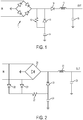
- Fig. 1 is one embodiment of a passive PFC circuit comprising a single diode bridge.
- the circuit converts an alternating current (AC) input voltage into a direct current (DC) output voltage.
- a first rectifying means rectifies the AC input voltage and provides a rectified voltage.
- a first capacitive means stores a first voltage.
- a resistive means applies the rectified voltage to the first capacitive means.
- a second capacitive means stores the DC output voltage.
- An inductive means applies the rectified voltage to the second capacitive means.
- a second rectifying means applies the first voltage to the inductive means.
- An optional diode prevents reverse energy flow from the second capacitive means to the first capacitive means.
- the AC input voltage is applied across a diode bridge 10.
- the rectified voltage thereof is applied to the cathode of a diode 11, the anode of an optional diode 16 and a resistor 12.
- the cathode of the diode 16 is connected to an inductor 13 and thus in series therewith.
- the diode 16 and the inductor 13 can be connected in the reverse order, wherein the cathode of the diode 11 can be connected to a tap of the inductor 13.
- the inductor 13 is further connected to an output capacitor 15 that stores the output voltage of the passive PFC circuit.
- a capacitor 14 is connected to the anode of the diode 11 and the resistor 12.
- the resistor 12 is thus in parallel with the diode 11.
- the diode bridge 10 and the capacitors 14 and 15 are grounded.
- the bridge 10 comprises two pairs of diodes.
- the cathodes of one pair are tied together and provide the rectified voltage.
- the anodes of the other pair are grounded.
- the AC input voltage is applied between anodes and cathodes of the pairs respectively, i.e., across each diode pair.
- the bridge 10 fully rectifies the input voltage.
- the capacitor 14 is charged through the resistor 12 and discharged through the parallel coupled diode 11. Therefore, charging and discharging the capacitor 14 increases and decreases the input current of the PFC circuit respectively.
- the input current drops to zero if the voltage stored in the capacitor 14 is larger than the rectified voltage, wherein the diode bridge 10 is cut off.
- this condition occurs only near the zero crossing of the AC input voltage. Therefore, the capacitor voltage is substantially equal to zero near the zero crossing of the AC input voltage.
- the voltage of the capacitor 14 can fall slightly below zero due to forward voltage drop of the bridge 10 unless the voltage drop across the diode 11 is the same or higher.
- the capacitor 14 is charged through the resistor 12. Therefore, the voltage stored in the capacitor 14 is smaller then the peak of the rectified voltage.
- the value of the capacitor 14 is chosen so that the input current drops to zero when the rectified voltage approaches zero, i.e. near zero crossing of the AC input voltage.
- the value of the inductor 13 is also sufficiently large so that the inductor 13 completes discharging the capacitor 14 near the zero crossing. Reverse polarity of the inductor current can be prevented by adding the diode 16.
- the inductor 13 is charged only when the rectified voltage is larger than the DC output voltage.
- the input current of the PFC circuit is equal to a difference between the current of the capacitor 14 and the inductor current.
- the AC input voltage and the inductor current are out of phase.
- the input current drops to zero near the zero crossing of the AC input voltage, whereas decreasing inductor current continues to flow.
- the inductor 13 completes discharging the capacitor 14 as the voltage stored therein reaches zero. Subsequently, the capacitor 14 is charged through the resistor 12. If the inductor 13 is too small, the inductor current may drop to zero before the zero crossing. If the inductor 13 is too large, the inductor current may substantially exceed charging current of the capacitor 14. In either case smaller power factor is accomplished.
- the resistor 12 is employed in order to smooth out the charging current of the capacitor 14.
- the capacitor 14 is discharged near the zero crossing of the AC input voltage.
- the resistor 12 carries the charging current so long as the rectified voltage is greater than the capacitor voltage, regardless of the inductor current. Therefore, the capacitor 14 is charged through the resistor 12 while the rectified voltage reaches its peak and subsequently drops to the level of the capacitor voltage. At this point the diode 11 starts to conduct and discharging of the capacitor 14 begins.
- the chosen value of the capacitor 14 allows the rate at which the capacitor voltage falls to match the rate of the AC input voltage before reaching the zero crossing. This is accomplished due to the resonant interaction between the inductor 13 and the capacitor 14.
- the bridge 10 conducts a portion of the inductor current. The inductor current reaches its peak after the peak of the rectified voltage. By contrast, the capacitor charging current and the rectified voltage reach their peaks simultaneously.
- the output capacitor 15 has a large value so that the output voltage has a small ripple.
- the output voltage may be considered constant.
- the capacitor 15 is charged entirely through the inductor 13.
- the inductor 13 carries the output current, wherein the output capacitor 15 acts as a buffer. Therefore, the RMS value of the inductor current is equal to the output current delivered to the load.
- the inductor current is unidirectional and continuous so that the current is constantly delivered to the output capacitor 15 regardless of the AC input voltage.
- the optional diode 16 is in series with the inductor 13 and thus rectifies the inductor current.
- the inductor current is unidirectional.
- the diode 16 can be used.
- a smaller inductance of the inductor 13 can be chosen in order to reduce its size and cost. In any case, the inductor current can prematurely drop to zero.
- the inductor current flows in the opposite direction after the voltage stored in the capacitor 14 falls below the output voltage of the passive PFC circuit. This reverse energy flow to the capacitor 14 from the output capacitor 15 reduces the efficiency of the passive PFC circuit. The power factor is diminished, wherein the input current only partially charges the capacitor 14.
- Fig. 2 is a preferred embodiment of a passive PFC circuit.
- the circuit converts an AC input voltage into a DC output voltage.
- a first rectifying means rectifies the AC input voltage and provides a first and second rectified voltages.
- a first capacitive means stores a first voltage.
- a resistive means applies the first rectified voltage to the first capacitive means.
- a second capacitive means stores the DC output voltage.
- An inductive means applies the second rectified voltage to the second capacitive means.
- a second rectifying means applies the first voltage to the inductive means.
- the AC input voltage is applied across a diode bridge 20 and between the anodes of a diode pair 26 and 27.
- the output voltage of the bridge 20 is applied to one end of an inductor 23 and the cathode of a diode 21.
- the other end of the inductor 23 is connected to an output capacitor 25 that stores the output voltage of the passive PFC circuit.
- the cathodes of the diodes 26, 27 and one end of a resistor 22 are tied together.
- a capacitor 24 is connected to the other end of the resistor 22 and the anode of the diode 21.
- the diode bridge 20 and the capacitors 24 and 25 are grounded.
- the bridge 20 fully rectifies the input voltage, which results in double frequency of the rectified voltage.
- the diode pair 26 and 27 performs the same function.
- the pair represents one half of another bridge that shares the pair of grounded diodes with the bridge 20. Consequently, voltages appearing at outputs of the bridge 20 and the pair 26, 27 can be independently higher than the absolute value of the AC input voltage.
- the inductor current is unidirectional.
- the capacitor 24 is fully discharged by the end of every cycle of the rectified input voltage. This is achieved by maintaining a sufficient current in the inductor 23. The capacitor 24 is thus charged through the diodes 26, 27 and discharged through the diode 21. The resistor 22 is employed in order to smooth out the charging current of the capacitor 24.
- the inductor 23 carries the entire output current, wherein the output capacitor 25 acts as a buffer.
- the output capacitor 25 is large so that the output voltage has a small ripple.
- the output voltage may be considered constant.
- the inductor 23 is charged whenever the voltage appearing at the output of the bridge 20 is greater than the output voltage. Otherwise the inductor 23 is discharged.
- the inductor current is continuous so that it is constantly delivered to the output capacitor 25, regardless of the AC input voltage.
- the peak value of the inductor current is smallest if the PFC circuit operates in the critical conduction mode.
- the inductor current reaches zero point, which is the boundary condition between continuous and discontinuous conduction modes.
- the DC component of the inductor current is equal to the amplitude of the AC component.
- the resistor 22 is employed to smooth out the input current after each zero crossing of the AC input voltage. Moreover, the resistor 22 allows the critically damped response of the resonant circuit. This circuit response results in the fastest possible decay without going into oscillation. Therefore, the desired state is reached as quickly as possible without overshooting.
- Fig. 4 is one embodiment of a passive PFC circuit comprising multiple outputs.
- the first rectifying means provides a plurality of rectified voltages.
- the second capacitive means comprises a plurality of third capacitive means for separately storing one of the DC output voltages.
- the inductive means comprises a plurality of second inductive means for separately applying one of the rectified voltages to one of the third capacitive means.
- the second rectifying means comprises a plurality of third rectifying means for separately applying the first voltage to one of the second inductive means.
- three diodes, one inductor and one capacitor are added.
- the first rectifying means comprises a plurality of second rectifying means for providing the plurality of the rectified voltages, and a third rectifying means coupled to ground for providing a ground reference.
- Each second rectifying means is coupled to the third rectifying means and comprises a pair of rectifiers providing the respective rectified voltage.
- the third rectifying means comprises a pair of rectifiers coupled to ground.
- the diode bridge 40 has 4 diodes connected as shown in the corresponding bridge 10 in Fig. 1 . Therefore, the second rectifying means comprises the diode pairs 46, 47 and 56, 57, and one half of the bridge 40 with the pair of diodes having cathodes connected to the diode 41 and the inductor 43.
- the third rectifying means is the other half of the bridge 40 with the pair of diodes having anodes connected to ground.
- the cathodes of the diodes 46, 47 and one end of the resistor 42 are tied together.
- a capacitor 44 is connected to the other end of the resistor 42 and the anodes of the diodes 41 and 51.
- the diode bridge 40 and the capacitors 44, 45 and 55 are grounded.
- any reference to “one aspect,” “an aspect,” “one embodiment,” or “an embodiment” means that a particular feature, structure, or characteristic described in connection with the aspect is included in at least one aspect.
- appearances of the phrases “in one aspect,” “in an aspect,” “in one embodiment,” or “in an embodiment” in various places throughout the specification are not necessarily all referring to the same aspect.
- the particular features, structures or characteristics may be combined in any suitable manner in one or more aspects or embodiments.
- electrical circuitry includes, but is not limited to, electrical circuitry having at least one discrete electrical circuit, electrical circuitry having at least one integrated circuit, electrical circuitry having at least one application specific integrated circuit.
- any two components so associated can also be viewed as being “operably connected,” or “operably coupled,” to each other to achieve the desired functionality, and any two components capable of being so associated can also be viewed as being “operably couplable,” to each other to achieve the desired functionality.
- operably couplable include but are not limited to physically mateable and/or physically interacting components, and/or wirelessly interactable, and/or wirelessly interacting components, and/or logically interacting, and/or logically interactable components.
Landscapes
- Engineering & Computer Science (AREA)
- Power Engineering (AREA)
- Rectifiers (AREA)
- Dc-Dc Converters (AREA)
Claims (11)
- Circuit de correction de facteur de puissance pour convertir une tension d'entrée à courant alternatif (AC) en au moins une tension de sortie à courant continu (DC), le circuit de correction de facteur de puissance comprenant:un premier moyen de redressement (10, 20, 26, 27, 30, 36, 37, 40, 46, 47) pour redresser la tension d'entrée AC (IN) et pour fournir une tension redressée;un premier moyen capacitif (14, 24, 34, 44) pour stocker une première tension;un premier moyen résistif (12, 22, 32, 42) pour appliquer la tension redressée au premier moyen capacitif (14, 24, 34, 44);un second moyen capacitif (15, 25, 35, 45) pour stocker la tension de sortie DC (OUT, OUT1);un premier moyen inductif (13, 23, 33, 43) pour appliquer la tension redressée au second moyen capacitif (15, 25, 35, 45); etun second moyen de redressement (11, 21, 31, 41) pour appliquer la première tension au premier moyen inductif (13, 23, 33, 43) ;dans lequel le premier moyen inductif (13, 23, 33, 43) et le premier moyen capacitif (14, 24, 34, 44) sont configurés pour avoir une interaction résonante et dans lequel le valeur du premier moyen inductif (13, 23, 33, 43) est tel que le déchargement du premier moyen capacitif (14, 24, 34, 44) soit complété près d'un passage à zéro de la tension d'entrée AC (IN).
- Circuit de correction de facteur de puissance selon la revendication 1, dans lequel le premier moyen inductif (13) conduit au moins un courant; et
le circuit de correction de facteur de puissance comprenant en outre un troisième moyen de redressement (16) pour redresser au moins l'un du premier moyen inductif (13) courants. - Circuit de correction de facteur de puissance selon la revendication 2, dans lequel le troisième moyen de redressement (16) est couplé en série avec le premier moyen inductif (13).
- Circuit de correction de facteur de puissance selon la revendication 1, comprenant en outre :un troisième moyen de redressement (56, 57) pour redresser la tension d'entrée AC (IN), dans lequel le premier moyen de redressement (10, 20, 26, 27, 30, 36, 37, 40, 46, 47) fournit une première tension redressée et le troisième moyen de redressement (56, 57) fournit une deuxième tension redressée ;un troisième moyen capacitif (55) pour stocker un deuxième tension de sortie DC (OUT2) ; etun second moyen inductif (53) pour appliquer une seconde tension redressée au troisième moyen capacitif (55) ;dans lequel le premier moyen résistif (12, 22, 32, 42) est arrangé pour appliquer la première tension redressée au premier moyen capacitif (14, 24, 34, 44); etdans lequel le second moyen inductif (53) est arrangé pour appliquer la seconde tension redressée au troisième moyen capacitif (55).
- Circuit de correction de facteur de puissance selon la revendication 1, comprenant en outre
un second moyen résistif (38, 39) couplé au premier moyen de redressement (30) et au second moyen de redressement (31) pour minimiser les oscillations parasites, dans lequel le second moyen résistif (38, 39) est couplé en parallèle avec le second moyen de redressement (31). - Circuit de correction de facteur de puissance selon la revendication 1, dans lequel le premier moyen de redressement (20, 26, 27, 30, 36, 37, 40, 46, 47) fournit une pluralité de tensions redressées;
dans lequel le deuxième moyen capacitif comprend une pluralité de moyens capacitifs (45, 55) pour stocker séparément au moins une des tensions de sortie DC (OUT1, OUT2);
dans lequel le premier moyen inductif comprend une pluralité de moyens inductifs (43, 53) pour appliquer séparément l'une des tensions redressées à l'un des moyens capacitifs (45, 55) ; et
dans lequel le second moyen de redressement comprend une pluralité de moyens de redressement (41, 51) pour appliquer séparément la première tension à l'un des moyens inductifs (43, 53). - Circuit de correction de facteur de puissance selon la revendication 1, dans lequel le premier moyen de redressement (10, 20, 26, 27, 30, 36, 37, 40, 46, 47), le premier moyen capacitif (14, 24, 34, 44) et le deuxième moyen capacitif (15, 25, 35, 45) sont couplés à la masse.
- Circuit de correction de facteur de puissance selon la revendication 1, dans lequel le premier moyen de redressement (10, 20, 26, 27, 30, 36, 37, 40, 46, 47) comprend une pluralité de moyen de redressement pour fournir une pluralité des tensions redressées; et au moins un moyen de redressement couplé à la masse pour fournir une référence de masse ;
dans lequel chaque premier moyen de redressement (10, 20, 26, 27, 30, 36, 37, 40, 46, 47) est couplé au deuxième moyen de redressement (11, 21, 31, 41). - Circuit de correction de facteur de puissance selon la revendication 1, dans lequel chaque premier moyen de redressement (10, 20, 26, 27, 30, 36, 37, 40, 46, 47) comprend au moins une paire de redresseurs (26, 27, 36, 37, 46, 47) fournissant la tension redressée respective.
- Circuit de correction de facteur de puissance selon la revendication 9, dans lequel chaque premier moyen de redressement (10, 20, 26, 27, 30, 36, 37, 40, 46, 47) comprend au moins une paire de redresseurs couplés à la masse.
- Circuit de correction de facteur de puissance selon la revendication 1, dans lequel la première tension est sensiblement égale à zéro près du passage à zéro de la tension d'entrée AC (IN).
Applications Claiming Priority (2)
| Application Number | Priority Date | Filing Date | Title |
|---|---|---|---|
| US13/647,979 US9143030B2 (en) | 2012-10-09 | 2012-10-09 | Passive power factor correction incorporating AC/DC conversion |
| PCT/US2013/063632 WO2014058753A2 (fr) | 2012-10-09 | 2013-10-07 | Correction passive du facteur de puissance intégrant une conversion ca/cc |
Publications (2)
| Publication Number | Publication Date |
|---|---|
| EP2907228A2 EP2907228A2 (fr) | 2015-08-19 |
| EP2907228B1 true EP2907228B1 (fr) | 2020-01-22 |
Family
ID=49447834
Family Applications (1)
| Application Number | Title | Priority Date | Filing Date |
|---|---|---|---|
| EP13779692.6A Active EP2907228B1 (fr) | 2012-10-09 | 2013-10-07 | Correction passive du facteur de puissance intégrant une conversion ca/cc |
Country Status (5)
| Country | Link |
|---|---|
| US (1) | US9143030B2 (fr) |
| EP (1) | EP2907228B1 (fr) |
| JP (1) | JP6353842B2 (fr) |
| KR (1) | KR102111144B1 (fr) |
| WO (1) | WO2014058753A2 (fr) |
Families Citing this family (12)
| Publication number | Priority date | Publication date | Assignee | Title |
|---|---|---|---|---|
| US9118185B2 (en) * | 2012-05-14 | 2015-08-25 | Qualcomm Incorporated | Systems and methods for high power factor charging |
| TWI492502B (zh) * | 2012-07-24 | 2015-07-11 | Ind Tech Res Inst | 被動式功因校正電路 |
| US9654024B2 (en) * | 2013-05-30 | 2017-05-16 | Texas Instruments Incorporated | AC-DC converter having soft-switched totem-pole output |
| EP3179575B1 (fr) * | 2014-08-05 | 2021-05-19 | Sony Corporation | Fiche ac/dc et équipement comprenant une telle fiche |
| CN105610135A (zh) * | 2016-03-30 | 2016-05-25 | 天津瑞能电气有限公司 | 一种应用于电力系统控制电源的保护装置 |
| CN108233715B (zh) * | 2018-02-27 | 2024-03-19 | 国网安徽省电力公司电力科学研究院 | 一种特高压直流发生器的一体化倍压整流筒 |
| TW202011660A (zh) * | 2018-09-07 | 2020-03-16 | 飛宏科技股份有限公司 | 多埠智能充電器 |
| EP3629465A1 (fr) * | 2018-09-26 | 2020-04-01 | Siemens Aktiengesellschaft | Système de conversion d'énergie électrique |
| FR3102897B1 (fr) * | 2019-10-30 | 2021-11-12 | St Microelectronics Tours Sas | Pont redresseur |
| CN113381601B (zh) * | 2020-03-09 | 2025-03-07 | 晶豪科技股份有限公司 | 具有emi防护功能的填谷式功率因子校正电路 |
| CN114597037B (zh) * | 2020-12-07 | 2025-08-08 | 广州视源电子科技股份有限公司 | 磁性器件及包含磁性器件的电路 |
| CN113676037B (zh) * | 2021-07-15 | 2024-03-08 | 朝阳微电子科技股份有限公司 | 一种无源功率因数校正方法 |
Citations (1)
| Publication number | Priority date | Publication date | Assignee | Title |
|---|---|---|---|---|
| WO2013074529A1 (fr) * | 2011-11-17 | 2013-05-23 | Qualcomm Incorporated | Systèmes, procédés et appareils pour un redresseur monophasé à facteur de puissance élevé |
Family Cites Families (26)
| Publication number | Priority date | Publication date | Assignee | Title |
|---|---|---|---|---|
| JPS5350914Y2 (fr) * | 1972-10-18 | 1978-12-06 | ||
| JPS55103082A (en) * | 1979-01-31 | 1980-08-06 | Toshiba Corp | Power rectification circuit |
| JPS5932214Y2 (ja) * | 1979-09-17 | 1984-09-10 | ティーディーケイ株式会社 | 寄生振動防止型整流平滑回路 |
| JPS59152991U (ja) * | 1983-03-31 | 1984-10-13 | 株式会社東芝 | 整流装置 |
| US4949234A (en) * | 1989-04-17 | 1990-08-14 | Zdzislaw Gulczynski | High efficiency power factor correction circuit |
| US5115185A (en) * | 1990-09-28 | 1992-05-19 | At&T Bell Laboratories | Single conversion power factor correction using septic converter |
| DE4237262A1 (de) | 1992-11-04 | 1994-05-05 | Patent Treuhand Ges Fuer Elektrische Gluehlampen Mbh | Schaltungsanordnung zum hochfrequenten Betrieb eines Verbrauchers |
| JPH06209574A (ja) | 1993-01-06 | 1994-07-26 | Sony Corp | 電源回路 |
| US5532917A (en) | 1993-02-17 | 1996-07-02 | Astec International, Ltd. | Power factor corrected rectifying circuit |
| JP3238266B2 (ja) * | 1994-01-28 | 2001-12-10 | 松下電器産業株式会社 | スイッチング電源装置 |
| US5561596A (en) * | 1994-02-22 | 1996-10-01 | International Business Machines Corporation | AC line stabilization circuitry for high power factor loads |
| JPH07284272A (ja) * | 1994-04-08 | 1995-10-27 | Nichicon Corp | 平滑回路 |
| JP3340240B2 (ja) * | 1994-04-25 | 2002-11-05 | ニチコン株式会社 | 倍電圧整流平滑回路 |
| GB2292270A (en) | 1994-08-12 | 1996-02-14 | Hitachi Consumer Products | ac to dc converter |
| FR2740627B1 (fr) * | 1995-10-30 | 1998-01-23 | Sgs Thomson Microelectronics | Alimentation a decoupage a correction de facteur de puissance |
| FR2743953B1 (fr) | 1996-01-19 | 1998-04-10 | Sgs Thomson Microelectronics | Circuit d'alimentation a condensateur de stockage |
| JPH1097601A (ja) * | 1996-09-20 | 1998-04-14 | Toshiba Corp | 情報記憶媒体 |
| US6043705A (en) * | 1998-03-25 | 2000-03-28 | Lucent Technologies Inc. | Boost converter having extended holdup time and method of operation |
| US6239992B1 (en) | 1999-06-09 | 2001-05-29 | Matsushita Refrigeration Company | Electric power unit with early auxiliary capacitor charging |
| TW200713762A (en) * | 2005-09-06 | 2007-04-01 | Acbel Polytech Inc | AC-DC converter capable of actively suppressing inrush current |
| TW200814501A (en) * | 2006-09-12 | 2008-03-16 | Delta Electronics Inc | Power adapter and power supply system using the same |
| JP5170096B2 (ja) * | 2007-07-09 | 2013-03-27 | 株式会社村田製作所 | Pfcコンバータ |
| US20100080026A1 (en) * | 2008-10-01 | 2010-04-01 | Xiaoyang Zhang | Power factor correction circuit |
| DE102009008635A1 (de) * | 2009-02-12 | 2010-08-19 | Osram Gesellschaft mit beschränkter Haftung | Schaltungsanordnung zum Umwandeln einer Eingangswechselspannung in eine Gleichspannung, Nachrüstlampe mit solch einer Schaltungsanordnung, sowie Beleuchtungssystem |
| US8129958B2 (en) * | 2009-03-25 | 2012-03-06 | Evergreen Micro Devices Co., Ltd. | Transition mode power factor correction device with built-in automatic total harmonic distortion reduction feature |
| KR101510181B1 (ko) * | 2010-09-06 | 2015-04-10 | 삼성전자 주식회사 | 전원공급회로 |
-
2012
- 2012-10-09 US US13/647,979 patent/US9143030B2/en active Active
-
2013
- 2013-10-07 EP EP13779692.6A patent/EP2907228B1/fr active Active
- 2013-10-07 KR KR1020157010617A patent/KR102111144B1/ko not_active Expired - Fee Related
- 2013-10-07 WO PCT/US2013/063632 patent/WO2014058753A2/fr not_active Ceased
- 2013-10-07 JP JP2015535857A patent/JP6353842B2/ja not_active Expired - Fee Related
Patent Citations (1)
| Publication number | Priority date | Publication date | Assignee | Title |
|---|---|---|---|---|
| WO2013074529A1 (fr) * | 2011-11-17 | 2013-05-23 | Qualcomm Incorporated | Systèmes, procédés et appareils pour un redresseur monophasé à facteur de puissance élevé |
Also Published As
| Publication number | Publication date |
|---|---|
| JP6353842B2 (ja) | 2018-07-04 |
| JP2015532576A (ja) | 2015-11-09 |
| US20140098584A1 (en) | 2014-04-10 |
| WO2014058753A2 (fr) | 2014-04-17 |
| WO2014058753A3 (fr) | 2014-08-28 |
| KR102111144B1 (ko) | 2020-05-15 |
| US9143030B2 (en) | 2015-09-22 |
| KR20150068407A (ko) | 2015-06-19 |
| EP2907228A2 (fr) | 2015-08-19 |
Similar Documents
| Publication | Publication Date | Title |
|---|---|---|
| US9143030B2 (en) | Passive power factor correction incorporating AC/DC conversion | |
| EP2448101B1 (fr) | Redresseur triphasé | |
| EP3208926B1 (fr) | Filtre actif et dispositif de conversion de courant alternatif en courant continu | |
| EP3101794A2 (fr) | Système de redresseur ca-cc | |
| EP1835609A1 (fr) | Circuit d'alimentation en courant multiphase, appareil d'entrainement, compresseur et climatiseur | |
| CN104704733A (zh) | 直接型电力转换装置以及直接型电力转换装置的控制方法 | |
| US20140029318A1 (en) | Passive power factor correction circuit | |
| CN206343741U (zh) | 焊机供电电路 | |
| CN104143902A (zh) | 一种能适应多种供电要求的电力电子变换器系统 | |
| Vishvanath et al. | Design and analysis of bridgeless zeta-derived power factor correction converter with reduced magnetic components | |
| US20100142238A1 (en) | Method and device in frequency converter | |
| Ohnuma et al. | A control method for a single-to-three-phase power converter with an active buffer and a charge circuit | |
| Chen et al. | Low-harmonic-input three-phase rectifier with passive auxiliary circuit: Comparison and design consideration | |
| CN1437310A (zh) | 无电磁污染的大功率开关电源装置 | |
| CN104079160B (zh) | 一种填谷电路 | |
| JP5175452B2 (ja) | インバータ装置 | |
| CN105099227B (zh) | 三相半波倍电压整流装置及电机驱动装置和空调器 | |
| Moon et al. | A high-performance 65 w universal ac-dc converter using a variable-inverter-rectifier-transformer with improved step-down capability | |
| CN208895359U (zh) | 供电焊接一体式电焊机及控制机构 | |
| CN201616768U (zh) | 一种中频电源电路 | |
| Liao et al. | Eliminating input electrolytic bulk capacitors in flyback-based universal chargers with a half-bridge series-stacked buffer | |
| US12062977B2 (en) | Electrical conversion apparatus for current shaping | |
| Choi et al. | A new unity power factor telecom rectifier system by an active waveshaping technique | |
| Maheshwari et al. | Performance Evaluation of Small DC-Link Capacitor Based Drive Under Grid Disturbance Conditions | |
| JPH079590Y2 (ja) | 整流平滑回路 |
Legal Events
| Date | Code | Title | Description |
|---|---|---|---|
| PUAI | Public reference made under article 153(3) epc to a published international application that has entered the european phase |
Free format text: ORIGINAL CODE: 0009012 |
|
| 17P | Request for examination filed |
Effective date: 20150417 |
|
| AK | Designated contracting states |
Kind code of ref document: A2 Designated state(s): AL AT BE BG CH CY CZ DE DK EE ES FI FR GB GR HR HU IE IS IT LI LT LU LV MC MK MT NL NO PL PT RO RS SE SI SK SM TR |
|
| AX | Request for extension of the european patent |
Extension state: BA ME |
|
| DAX | Request for extension of the european patent (deleted) | ||
| RAP1 | Party data changed (applicant data changed or rights of an application transferred) |
Owner name: TELEDYNE TECHNOLOGIES INCORPORATED |
|
| RAP1 | Party data changed (applicant data changed or rights of an application transferred) |
Owner name: SEOUL SEMICONDUCTOR CO., LTD. |
|
| GRAP | Despatch of communication of intention to grant a patent |
Free format text: ORIGINAL CODE: EPIDOSNIGR1 |
|
| STAA | Information on the status of an ep patent application or granted ep patent |
Free format text: STATUS: GRANT OF PATENT IS INTENDED |
|
| INTG | Intention to grant announced |
Effective date: 20190514 |
|
| GRAJ | Information related to disapproval of communication of intention to grant by the applicant or resumption of examination proceedings by the epo deleted |
Free format text: ORIGINAL CODE: EPIDOSDIGR1 |
|
| STAA | Information on the status of an ep patent application or granted ep patent |
Free format text: STATUS: REQUEST FOR EXAMINATION WAS MADE |
|
| GRAS | Grant fee paid |
Free format text: ORIGINAL CODE: EPIDOSNIGR3 |
|
| STAA | Information on the status of an ep patent application or granted ep patent |
Free format text: STATUS: GRANT OF PATENT IS INTENDED |
|
| GRAP | Despatch of communication of intention to grant a patent |
Free format text: ORIGINAL CODE: EPIDOSNIGR1 |
|
| INTC | Intention to grant announced (deleted) | ||
| INTG | Intention to grant announced |
Effective date: 20191008 |
|
| GRAA | (expected) grant |
Free format text: ORIGINAL CODE: 0009210 |
|
| STAA | Information on the status of an ep patent application or granted ep patent |
Free format text: STATUS: THE PATENT HAS BEEN GRANTED |
|
| AK | Designated contracting states |
Kind code of ref document: B1 Designated state(s): AL AT BE BG CH CY CZ DE DK EE ES FI FR GB GR HR HU IE IS IT LI LT LU LV MC MK MT NL NO PL PT RO RS SE SI SK SM TR |
|
| REG | Reference to a national code |
Ref country code: GB Ref legal event code: FG4D |
|
| REG | Reference to a national code |
Ref country code: CH Ref legal event code: EP |
|
| REG | Reference to a national code |
Ref country code: AT Ref legal event code: REF Ref document number: 1227586 Country of ref document: AT Kind code of ref document: T Effective date: 20200215 |
|
| REG | Reference to a national code |
Ref country code: IE Ref legal event code: FG4D |
|
| REG | Reference to a national code |
Ref country code: DE Ref legal event code: R096 Ref document number: 602013065321 Country of ref document: DE |
|
| REG | Reference to a national code |
Ref country code: NL Ref legal event code: FP |
|
| REG | Reference to a national code |
Ref country code: LT Ref legal event code: MG4D |
|
| PG25 | Lapsed in a contracting state [announced via postgrant information from national office to epo] |
Ref country code: NO Free format text: LAPSE BECAUSE OF FAILURE TO SUBMIT A TRANSLATION OF THE DESCRIPTION OR TO PAY THE FEE WITHIN THE PRESCRIBED TIME-LIMIT Effective date: 20200422 Ref country code: FI Free format text: LAPSE BECAUSE OF FAILURE TO SUBMIT A TRANSLATION OF THE DESCRIPTION OR TO PAY THE FEE WITHIN THE PRESCRIBED TIME-LIMIT Effective date: 20200122 Ref country code: PT Free format text: LAPSE BECAUSE OF FAILURE TO SUBMIT A TRANSLATION OF THE DESCRIPTION OR TO PAY THE FEE WITHIN THE PRESCRIBED TIME-LIMIT Effective date: 20200614 Ref country code: RS Free format text: LAPSE BECAUSE OF FAILURE TO SUBMIT A TRANSLATION OF THE DESCRIPTION OR TO PAY THE FEE WITHIN THE PRESCRIBED TIME-LIMIT Effective date: 20200122 |
|
| PG25 | Lapsed in a contracting state [announced via postgrant information from national office to epo] |
Ref country code: GR Free format text: LAPSE BECAUSE OF FAILURE TO SUBMIT A TRANSLATION OF THE DESCRIPTION OR TO PAY THE FEE WITHIN THE PRESCRIBED TIME-LIMIT Effective date: 20200423 Ref country code: BG Free format text: LAPSE BECAUSE OF FAILURE TO SUBMIT A TRANSLATION OF THE DESCRIPTION OR TO PAY THE FEE WITHIN THE PRESCRIBED TIME-LIMIT Effective date: 20200422 Ref country code: LV Free format text: LAPSE BECAUSE OF FAILURE TO SUBMIT A TRANSLATION OF THE DESCRIPTION OR TO PAY THE FEE WITHIN THE PRESCRIBED TIME-LIMIT Effective date: 20200122 Ref country code: SE Free format text: LAPSE BECAUSE OF FAILURE TO SUBMIT A TRANSLATION OF THE DESCRIPTION OR TO PAY THE FEE WITHIN THE PRESCRIBED TIME-LIMIT Effective date: 20200122 Ref country code: IS Free format text: LAPSE BECAUSE OF FAILURE TO SUBMIT A TRANSLATION OF THE DESCRIPTION OR TO PAY THE FEE WITHIN THE PRESCRIBED TIME-LIMIT Effective date: 20200522 Ref country code: HR Free format text: LAPSE BECAUSE OF FAILURE TO SUBMIT A TRANSLATION OF THE DESCRIPTION OR TO PAY THE FEE WITHIN THE PRESCRIBED TIME-LIMIT Effective date: 20200122 |
|
| REG | Reference to a national code |
Ref country code: DE Ref legal event code: R097 Ref document number: 602013065321 Country of ref document: DE |
|
| PG25 | Lapsed in a contracting state [announced via postgrant information from national office to epo] |
Ref country code: DK Free format text: LAPSE BECAUSE OF FAILURE TO SUBMIT A TRANSLATION OF THE DESCRIPTION OR TO PAY THE FEE WITHIN THE PRESCRIBED TIME-LIMIT Effective date: 20200122 Ref country code: SM Free format text: LAPSE BECAUSE OF FAILURE TO SUBMIT A TRANSLATION OF THE DESCRIPTION OR TO PAY THE FEE WITHIN THE PRESCRIBED TIME-LIMIT Effective date: 20200122 Ref country code: SK Free format text: LAPSE BECAUSE OF FAILURE TO SUBMIT A TRANSLATION OF THE DESCRIPTION OR TO PAY THE FEE WITHIN THE PRESCRIBED TIME-LIMIT Effective date: 20200122 Ref country code: EE Free format text: LAPSE BECAUSE OF FAILURE TO SUBMIT A TRANSLATION OF THE DESCRIPTION OR TO PAY THE FEE WITHIN THE PRESCRIBED TIME-LIMIT Effective date: 20200122 Ref country code: CZ Free format text: LAPSE BECAUSE OF FAILURE TO SUBMIT A TRANSLATION OF THE DESCRIPTION OR TO PAY THE FEE WITHIN THE PRESCRIBED TIME-LIMIT Effective date: 20200122 Ref country code: RO Free format text: LAPSE BECAUSE OF FAILURE TO SUBMIT A TRANSLATION OF THE DESCRIPTION OR TO PAY THE FEE WITHIN THE PRESCRIBED TIME-LIMIT Effective date: 20200122 Ref country code: LT Free format text: LAPSE BECAUSE OF FAILURE TO SUBMIT A TRANSLATION OF THE DESCRIPTION OR TO PAY THE FEE WITHIN THE PRESCRIBED TIME-LIMIT Effective date: 20200122 Ref country code: ES Free format text: LAPSE BECAUSE OF FAILURE TO SUBMIT A TRANSLATION OF THE DESCRIPTION OR TO PAY THE FEE WITHIN THE PRESCRIBED TIME-LIMIT Effective date: 20200122 |
|
| REG | Reference to a national code |
Ref country code: AT Ref legal event code: MK05 Ref document number: 1227586 Country of ref document: AT Kind code of ref document: T Effective date: 20200122 |
|
| PLBE | No opposition filed within time limit |
Free format text: ORIGINAL CODE: 0009261 |
|
| STAA | Information on the status of an ep patent application or granted ep patent |
Free format text: STATUS: NO OPPOSITION FILED WITHIN TIME LIMIT |
|
| 26N | No opposition filed |
Effective date: 20201023 |
|
| PG25 | Lapsed in a contracting state [announced via postgrant information from national office to epo] |
Ref country code: IT Free format text: LAPSE BECAUSE OF FAILURE TO SUBMIT A TRANSLATION OF THE DESCRIPTION OR TO PAY THE FEE WITHIN THE PRESCRIBED TIME-LIMIT Effective date: 20200122 Ref country code: AT Free format text: LAPSE BECAUSE OF FAILURE TO SUBMIT A TRANSLATION OF THE DESCRIPTION OR TO PAY THE FEE WITHIN THE PRESCRIBED TIME-LIMIT Effective date: 20200122 |
|
| PG25 | Lapsed in a contracting state [announced via postgrant information from national office to epo] |
Ref country code: PL Free format text: LAPSE BECAUSE OF FAILURE TO SUBMIT A TRANSLATION OF THE DESCRIPTION OR TO PAY THE FEE WITHIN THE PRESCRIBED TIME-LIMIT Effective date: 20200122 Ref country code: SI Free format text: LAPSE BECAUSE OF FAILURE TO SUBMIT A TRANSLATION OF THE DESCRIPTION OR TO PAY THE FEE WITHIN THE PRESCRIBED TIME-LIMIT Effective date: 20200122 |
|
| REG | Reference to a national code |
Ref country code: CH Ref legal event code: PL |
|
| PG25 | Lapsed in a contracting state [announced via postgrant information from national office to epo] |
Ref country code: LU Free format text: LAPSE BECAUSE OF NON-PAYMENT OF DUE FEES Effective date: 20201007 Ref country code: MC Free format text: LAPSE BECAUSE OF FAILURE TO SUBMIT A TRANSLATION OF THE DESCRIPTION OR TO PAY THE FEE WITHIN THE PRESCRIBED TIME-LIMIT Effective date: 20200122 |
|
| REG | Reference to a national code |
Ref country code: BE Ref legal event code: MM Effective date: 20201031 |
|
| PG25 | Lapsed in a contracting state [announced via postgrant information from national office to epo] |
Ref country code: FR Free format text: LAPSE BECAUSE OF NON-PAYMENT OF DUE FEES Effective date: 20201031 |
|
| PG25 | Lapsed in a contracting state [announced via postgrant information from national office to epo] |
Ref country code: LI Free format text: LAPSE BECAUSE OF NON-PAYMENT OF DUE FEES Effective date: 20201031 Ref country code: CH Free format text: LAPSE BECAUSE OF NON-PAYMENT OF DUE FEES Effective date: 20201031 Ref country code: BE Free format text: LAPSE BECAUSE OF NON-PAYMENT OF DUE FEES Effective date: 20201031 |
|
| PG25 | Lapsed in a contracting state [announced via postgrant information from national office to epo] |
Ref country code: IE Free format text: LAPSE BECAUSE OF NON-PAYMENT OF DUE FEES Effective date: 20201007 |
|
| PG25 | Lapsed in a contracting state [announced via postgrant information from national office to epo] |
Ref country code: TR Free format text: LAPSE BECAUSE OF FAILURE TO SUBMIT A TRANSLATION OF THE DESCRIPTION OR TO PAY THE FEE WITHIN THE PRESCRIBED TIME-LIMIT Effective date: 20200122 Ref country code: MT Free format text: LAPSE BECAUSE OF FAILURE TO SUBMIT A TRANSLATION OF THE DESCRIPTION OR TO PAY THE FEE WITHIN THE PRESCRIBED TIME-LIMIT Effective date: 20200122 Ref country code: CY Free format text: LAPSE BECAUSE OF FAILURE TO SUBMIT A TRANSLATION OF THE DESCRIPTION OR TO PAY THE FEE WITHIN THE PRESCRIBED TIME-LIMIT Effective date: 20200122 |
|
| PG25 | Lapsed in a contracting state [announced via postgrant information from national office to epo] |
Ref country code: MK Free format text: LAPSE BECAUSE OF FAILURE TO SUBMIT A TRANSLATION OF THE DESCRIPTION OR TO PAY THE FEE WITHIN THE PRESCRIBED TIME-LIMIT Effective date: 20200122 Ref country code: AL Free format text: LAPSE BECAUSE OF FAILURE TO SUBMIT A TRANSLATION OF THE DESCRIPTION OR TO PAY THE FEE WITHIN THE PRESCRIBED TIME-LIMIT Effective date: 20200122 |
|
| PGFP | Annual fee paid to national office [announced via postgrant information from national office to epo] |
Ref country code: NL Payment date: 20220822 Year of fee payment: 10 |
|
| PGFP | Annual fee paid to national office [announced via postgrant information from national office to epo] |
Ref country code: GB Payment date: 20220822 Year of fee payment: 10 |
|
| PGFP | Annual fee paid to national office [announced via postgrant information from national office to epo] |
Ref country code: DE Payment date: 20220822 Year of fee payment: 10 |
|
| REG | Reference to a national code |
Ref country code: DE Ref legal event code: R119 Ref document number: 602013065321 Country of ref document: DE |
|
| REG | Reference to a national code |
Ref country code: NL Ref legal event code: MM Effective date: 20231101 |
|
| GBPC | Gb: european patent ceased through non-payment of renewal fee |
Effective date: 20231007 |
|
| PG25 | Lapsed in a contracting state [announced via postgrant information from national office to epo] |
Ref country code: GB Free format text: LAPSE BECAUSE OF NON-PAYMENT OF DUE FEES Effective date: 20231007 |
|
| PG25 | Lapsed in a contracting state [announced via postgrant information from national office to epo] |
Ref country code: NL Free format text: LAPSE BECAUSE OF NON-PAYMENT OF DUE FEES Effective date: 20231101 |
|
| PG25 | Lapsed in a contracting state [announced via postgrant information from national office to epo] |
Ref country code: NL Free format text: LAPSE BECAUSE OF NON-PAYMENT OF DUE FEES Effective date: 20231101 Ref country code: GB Free format text: LAPSE BECAUSE OF NON-PAYMENT OF DUE FEES Effective date: 20231007 Ref country code: DE Free format text: LAPSE BECAUSE OF NON-PAYMENT OF DUE FEES Effective date: 20240501 |