EP2908121A1 - Capteur de gaz et procédé destiné à la détection de gaz - Google Patents
Capteur de gaz et procédé destiné à la détection de gaz Download PDFInfo
- Publication number
- EP2908121A1 EP2908121A1 EP15000410.9A EP15000410A EP2908121A1 EP 2908121 A1 EP2908121 A1 EP 2908121A1 EP 15000410 A EP15000410 A EP 15000410A EP 2908121 A1 EP2908121 A1 EP 2908121A1
- Authority
- EP
- European Patent Office
- Prior art keywords
- nanofibers
- gas
- gas sensor
- sensors
- electrical resistance
- Prior art date
- Legal status (The legal status is an assumption and is not a legal conclusion. Google has not performed a legal analysis and makes no representation as to the accuracy of the status listed.)
- Withdrawn
Links
- 239000007789 gas Substances 0.000 title claims abstract description 198
- 238000000034 method Methods 0.000 title claims description 26
- 238000001514 detection method Methods 0.000 title claims description 15
- 239000002121 nanofiber Substances 0.000 claims abstract description 163
- 239000000463 material Substances 0.000 claims abstract description 39
- 239000000203 mixture Substances 0.000 claims description 18
- 239000000758 substrate Substances 0.000 claims description 18
- 229910021418 black silicon Inorganic materials 0.000 claims description 14
- 238000004519 manufacturing process Methods 0.000 claims description 11
- 238000011156 evaluation Methods 0.000 claims description 6
- 238000009833 condensation Methods 0.000 claims description 3
- 230000005494 condensation Effects 0.000 claims description 3
- 238000003491 array Methods 0.000 claims 1
- 230000004044 response Effects 0.000 description 19
- 230000035945 sensitivity Effects 0.000 description 17
- 238000010586 diagram Methods 0.000 description 15
- 230000004913 activation Effects 0.000 description 13
- 235000019645 odor Nutrition 0.000 description 13
- 230000008569 process Effects 0.000 description 12
- 238000010438 heat treatment Methods 0.000 description 9
- 229910044991 metal oxide Inorganic materials 0.000 description 9
- 150000004706 metal oxides Chemical class 0.000 description 9
- BASFCYQUMIYNBI-UHFFFAOYSA-N platinum Chemical compound [Pt] BASFCYQUMIYNBI-UHFFFAOYSA-N 0.000 description 6
- 230000005855 radiation Effects 0.000 description 6
- 238000011084 recovery Methods 0.000 description 6
- XOLBLPGZBRYERU-UHFFFAOYSA-N tin dioxide Chemical compound O=[Sn]=O XOLBLPGZBRYERU-UHFFFAOYSA-N 0.000 description 6
- XUIMIQQOPSSXEZ-UHFFFAOYSA-N Silicon Chemical compound [Si] XUIMIQQOPSSXEZ-UHFFFAOYSA-N 0.000 description 5
- 238000004458 analytical method Methods 0.000 description 5
- 229910052710 silicon Inorganic materials 0.000 description 5
- 229910006404 SnO 2 Inorganic materials 0.000 description 4
- 239000000919 ceramic Substances 0.000 description 4
- 230000001419 dependent effect Effects 0.000 description 4
- 238000013461 design Methods 0.000 description 4
- 238000002474 experimental method Methods 0.000 description 4
- 230000006870 function Effects 0.000 description 4
- 230000001590 oxidative effect Effects 0.000 description 4
- 239000010703 silicon Substances 0.000 description 4
- VYPSYNLAJGMNEJ-UHFFFAOYSA-N silicon dioxide Inorganic materials O=[Si]=O VYPSYNLAJGMNEJ-UHFFFAOYSA-N 0.000 description 4
- 230000008859 change Effects 0.000 description 3
- 230000007423 decrease Effects 0.000 description 3
- 229910052697 platinum Inorganic materials 0.000 description 3
- 238000001878 scanning electron micrograph Methods 0.000 description 3
- 235000012239 silicon dioxide Nutrition 0.000 description 3
- 239000000779 smoke Substances 0.000 description 3
- XKRFYHLGVUSROY-UHFFFAOYSA-N Argon Chemical compound [Ar] XKRFYHLGVUSROY-UHFFFAOYSA-N 0.000 description 2
- 230000003213 activating effect Effects 0.000 description 2
- 229910052786 argon Inorganic materials 0.000 description 2
- 238000000576 coating method Methods 0.000 description 2
- 230000003750 conditioning effect Effects 0.000 description 2
- 238000005530 etching Methods 0.000 description 2
- 239000003365 glass fiber Substances 0.000 description 2
- 238000005259 measurement Methods 0.000 description 2
- 238000001451 molecular beam epitaxy Methods 0.000 description 2
- 229910052760 oxygen Inorganic materials 0.000 description 2
- 238000001020 plasma etching Methods 0.000 description 2
- 239000010453 quartz Substances 0.000 description 2
- 230000035484 reaction time Effects 0.000 description 2
- 230000009467 reduction Effects 0.000 description 2
- 230000001105 regulatory effect Effects 0.000 description 2
- 229910004298 SiO 2 Inorganic materials 0.000 description 1
- -1 SnO 2 are arranged Chemical class 0.000 description 1
- 229910010413 TiO 2 Inorganic materials 0.000 description 1
- 229910052782 aluminium Inorganic materials 0.000 description 1
- XAGFODPZIPBFFR-UHFFFAOYSA-N aluminium Chemical compound [Al] XAGFODPZIPBFFR-UHFFFAOYSA-N 0.000 description 1
- 239000012080 ambient air Substances 0.000 description 1
- QVGXLLKOCUKJST-UHFFFAOYSA-N atomic oxygen Chemical compound [O] QVGXLLKOCUKJST-UHFFFAOYSA-N 0.000 description 1
- 230000015572 biosynthetic process Effects 0.000 description 1
- 239000011248 coating agent Substances 0.000 description 1
- 238000001816 cooling Methods 0.000 description 1
- 239000013078 crystal Substances 0.000 description 1
- 229910021419 crystalline silicon Inorganic materials 0.000 description 1
- 230000003247 decreasing effect Effects 0.000 description 1
- 238000000151 deposition Methods 0.000 description 1
- 238000011161 development Methods 0.000 description 1
- 230000000694 effects Effects 0.000 description 1
- 238000005265 energy consumption Methods 0.000 description 1
- 230000005284 excitation Effects 0.000 description 1
- 239000000835 fiber Substances 0.000 description 1
- 210000004602 germ cell Anatomy 0.000 description 1
- 238000001198 high resolution scanning electron microscopy Methods 0.000 description 1
- 238000005286 illumination Methods 0.000 description 1
- 239000011261 inert gas Substances 0.000 description 1
- 150000002500 ions Chemical class 0.000 description 1
- 230000001678 irradiating effect Effects 0.000 description 1
- 239000007788 liquid Substances 0.000 description 1
- 238000001755 magnetron sputter deposition Methods 0.000 description 1
- 238000002156 mixing Methods 0.000 description 1
- 230000004048 modification Effects 0.000 description 1
- 238000012986 modification Methods 0.000 description 1
- 239000002071 nanotube Substances 0.000 description 1
- 229910052756 noble gas Inorganic materials 0.000 description 1
- 150000002835 noble gases Chemical class 0.000 description 1
- 239000001301 oxygen Substances 0.000 description 1
- 239000000843 powder Substances 0.000 description 1
- 239000002243 precursor Substances 0.000 description 1
- 239000004065 semiconductor Substances 0.000 description 1
- 239000000377 silicon dioxide Substances 0.000 description 1
- 238000001429 visible spectrum Methods 0.000 description 1
Images


Classifications
-
- G—PHYSICS
- G01—MEASURING; TESTING
- G01N—INVESTIGATING OR ANALYSING MATERIALS BY DETERMINING THEIR CHEMICAL OR PHYSICAL PROPERTIES
- G01N27/00—Investigating or analysing materials by the use of electric, electrochemical, or magnetic means
- G01N27/02—Investigating or analysing materials by the use of electric, electrochemical, or magnetic means by investigating impedance
- G01N27/04—Investigating or analysing materials by the use of electric, electrochemical, or magnetic means by investigating impedance by investigating resistance
- G01N27/12—Investigating or analysing materials by the use of electric, electrochemical, or magnetic means by investigating impedance by investigating resistance of a solid body in dependence upon absorption of a fluid; of a solid body in dependence upon reaction with a fluid, for detecting components in the fluid
- G01N27/125—Composition of the body, e.g. the composition of its sensitive layer
- G01N27/127—Composition of the body, e.g. the composition of its sensitive layer comprising nanoparticles
-
- B—PERFORMING OPERATIONS; TRANSPORTING
- B82—NANOTECHNOLOGY
- B82Y—SPECIFIC USES OR APPLICATIONS OF NANOSTRUCTURES; MEASUREMENT OR ANALYSIS OF NANOSTRUCTURES; MANUFACTURE OR TREATMENT OF NANOSTRUCTURES
- B82Y30/00—Nanotechnology for materials or surface science, e.g. nanocomposites
-
- G—PHYSICS
- G01—MEASURING; TESTING
- G01N—INVESTIGATING OR ANALYSING MATERIALS BY DETERMINING THEIR CHEMICAL OR PHYSICAL PROPERTIES
- G01N33/00—Investigating or analysing materials by specific methods not covered by groups G01N1/00 - G01N31/00
- G01N33/0004—Gaseous mixtures, e.g. polluted air
- G01N33/0009—General constructional details of gas analysers, e.g. portable test equipment
- G01N33/0027—General constructional details of gas analysers, e.g. portable test equipment concerning the detector
- G01N33/0031—General constructional details of gas analysers, e.g. portable test equipment concerning the detector comprising two or more sensors, e.g. a sensor array
Definitions
- the invention relates to a gas sensor for the detection of gases and to a method for the detection of gases.
- a conventional gas sensor is known, for example, under the name KAMINA, the Karlsroner Mikronase.
- the document EP 0 769 141 relates to a gas sensor which serves to detect odors and for this purpose has a plurality of partial sensors, all of which differ slightly from one another.
- Each of the component sensors has a layer of gas-sensitive material, for example a layer of one or more semiconductive oxides, such as tin dioxide.
- the electrical resistance of the layer of tin dioxide changes when the layer is in contact with a reducing or oxidizing gas. This change in electrical resistance is measured and evaluated.
- Each of the sub-sensors differs slightly from the other sub-sensors, for example, by different thickness coatings with an additional material, such as SiO 2 . Since the sensitivity of the partial sensor relative to the gas to be detected is dependent on the layer thickness, the different partial sensors react with different degrees of change in resistance to gases to be detected. As a result, the different partial sensors of the gas sensor are suitable for detecting different gas mixtures and for example classifying them in "odors", for which reason such a gas sensor is also referred to as "nose”.
- the gas-sensitive layer of tin dioxide must be "activated", ie the gas-sensitive layer must be in a state in which the electrical Resistance of the gas-sensitive layer is in a strong dependence on the gas mixture surrounding the gas-sensitive layer. For activation, it is therefore necessary to heat the gas-sensitive layer. Activation temperatures of over 200 ° C or over 250 ° C are required.
- Such conventional gas sensors have several disadvantages.
- the additional design effort the provision of a heating conditional, the operating costs of the gas sensor are high, since the gas sensor is operational only in a highly heated state.
- the resistance of the part sensors is highly dependent on the temperature, which is why a very accurate and expensive temperature control is necessary to set the part sensors to a predetermined temperature.
- the energy consumption of a conventional gas sensor is so high that a battery operation of the gas sensor is almost impossible. This complicates the use of such a gas sensor as e.g. Smoke detector.
- Both the gas sensors with the metal oxide layer and the gas sensors with the nanofibers are expensive to condition, either by a temperature controlled via the heater, on the part sensors temperature gradient or by different strong nanofiber densities or thicknesses or different coating thicknesses. This conditioning of the different part sensors is both costly and inaccurate.
- the invention has for its object to provide an improved gas sensor for detecting gases, in particular a gas sensor which attenuates at least one of the disadvantages described above.
- One aspect relates to a gas sensor that is designed for the detection of gases and has a plurality of partial sensors, each having a gas-sensitive material with a certain measurable electrical resistance. At least one of the partial sensors has nanofibers as the gas-sensitive material. The nanofibers are designed so that the electrical resistance of the nanofibers can be changed by light irradiation. The light irradiation reduces the electrical resistance of the nanofibers and replaces the activation of the fibers by high temperatures used in conventional sensors.
- the gas sensor is used in particular for the detection of reducing or oxidizing gases, while it may be unsuitable for the detection of inert gases or noble gases.
- the partial sensors of the gas sensor can each differ slightly from each other.
- the part sensors differ in their sensitivity from each other, i. the individual part sensors change their electrical resistance to different degrees when they are in contact with a specific gas or gas mixture.
- the gas sensor is suitable for "odor detection” or for the detection of different gases and / or gas mixtures in different compositions.
- a method can be provided which is based on a mathematical algorithm.
- a measured constellation e.g. a measured "pattern" of electrical resistances at the different sub-sensors, compared to pre-stored constellations or "patterns".
- the gas sensor can be trained and / or sensitized to certain odors.
- the electrical resistance of the gas sensitive materials of the part sensors is measurable.
- the current flowing through the sub-sensor current can be measured and / or the voltage applied to the sub-sensor.
- a measurement of the electrical resistance comprises a measurement of the electrical conductivity of the gas-sensitive material.
- the gas sensor may comprise a plurality of electrodes, of which at least one electrode is in electrical contact with at least one of the component sensors, so that the electrical resistance of the gas-sensitive material of the at least one component sensor can be measured.
- the electrodes serve to electrically contact the component sensors.
- all the electrodes can be formed in an electrical contact with at least one partial sensor.
- the gas-sensitive material of each sub-sensor is in electrical contact with two electrodes, so that the electrical resistance of the sub-sensor can be measured by the current flow between these two electrodes.
- the individual electrodes can be arranged, for example, in a boundary region of two adjacent partial sensors such that two adjacent partial sensors are contacted by the same electrode. This reduces the total number of electrodes required because one electrode can be used to measure the electrical resistance of second different adjacent sub-sensors.
- nanofibers are provided.
- the nanofibers may be formed from a metal oxide that chemically reacts with gas mixtures in the environment.
- the nanofibers can be formed from one or more semiconductive metal oxide (s), for example from SnO 2 and / or other metal oxides, whose band gap between valence and conduction band is so low that excitation by means of light or UV light can take place.
- s semiconductive metal oxide
- These include, for example, WO 3 , ZnO, TiO 2 , V 2 O 5 or In 2 O 3 .
- the diameters of the nanofibers are strong between 10 nm and 2000 nm.
- each sub-sensor has at least as many nanofibers that the electrodes provided for measuring the electrical resistance of the sub-sensor are in electrical contact with one another via the nanofibers.
- nanotubes can also be used.
- the gas sensor has a light source for targeted illumination of the nanofibers.
- the light source may be oriented so that the light emission of the light source is directed to the component sensors.
- the activation of the gas-sensitive materials takes place in the gas sensor thus by light irradiation.
- the light need not be from the visible spectrum, but may be non-visible light, especially UV light.
- the wavelength of the light irradiation can be matched to the material of the nanofibers, so that the energy of the incident photons is suitable for reducing the electrical resistance of the nanofibers.
- nanofibers of a semiconducting material e.g. a wavelength of light irradiation corresponding to a photon energy value between 50% and 150% of the band gap.
- the light source may either directly irradiate the sub-sensors or the light may be redirected by means of a glass fiber, mirrors and / or prisms so as to irradiate the sub-sensors.
- the light source or the glass fiber output is preferably between 1 mm and 10 cm spaced from the part sensors arranged, more preferably between 5 mm and 2 cm spaced.
- a light source to activate the gas sensor eliminates the need to provide a heater to activate the part sensors.
- a heater may additionally be provided, e.g. for a fine adjustment of the sensitivity of the individual part sensors, however, a heating by the use of the light irradiation is not necessary for the operation of the gas sensor.
- By activating the partial sensors by means of light irradiation heating is superfluous. This causes a significant energy reduction in the operation of the gas sensor.
- the gas sensor can be operated in battery mode.
- the electrical resistance of the nanofibers is reduced by at least 50% as compared to the electrical resistance of the nanofibers without light irradiation by the light source.
- the electrical resistance is reduced by the light irradiation by at least 90%, so that gases can be detected more easily.
- a reduction in the electrical resistance of the nanofibers corresponds to activation of the gas sensor and increases the sensitivity of the gas sensor for the detection of gases.
- the light source is designed as a UV light source.
- the activation of the nanofibers takes place by light irradiation with UV light.
- UV light has a wavelength of 10 nm to 400 nm.
- a light irradiation with light having a wavelength of 300 nm to 400 nm preferably takes place.
- the resistance of the nanofibers can be particularly greatly reduced by the light irradiation with UV light. This is why UV light is particularly suitable for activating the partial sensors.
- the light source can be designed as a UV LED that emits light particularly energy efficient and precisely adjustable.
- the sub-sensors are heated to a maximum of 100 ° C, preferably heated to a maximum of 50 ° C.
- the gas sensor is operated at room temperature such that the activation of the nanofibers is substantially independent of the ambient temperature.
- the gas sensor can be activated in particular at room temperature without a heater. The operation of the gas sensor at these low temperatures is particularly energy-efficient and therefore cost, especially in continuous operation.
- the light irradiation is performed by the light source with a Power in a range of 0.1 mW / cm 2 to 250 mW / cm 2.
- the light irradiation may preferably be performed at a power in a range of 2.0 mW / cm 2 to 10 mW / cm 2 , more preferably in one range from 2.5 mW / cm 2 to 10 mW / cm 2 . 2.
- the light irradiation may also be performed at a power in a range of 0.1 mW / cm 2 to 50 mW / cm 2 , more preferably in a range of 0.1 mW / cm 2 to 10 mW / cm 2 , more preferably in a range of 0.4 mW / cm 2 to 4 mW / cm 2 .
- Even the light irradiation with this low power is sufficient to lower the electrical resistance to activate the gas sensor sufficiently. This makes it possible to provide a particularly energy-saving gas sensor, which is low in operation.
- the gas sensor can save both energy, since it can be operated at low temperatures, and because the light irradiation requires very little power.
- the gas sensor can be designed and provided at this low power consumption to be operated by means of a battery as an energy source.
- the gas sensor has a substantially contiguous layer of nanofibers as the gas-sensitive material, wherein the layer of nanofibers is subdivided by a plurality of electrodes into fields such that a field of the layer of nanofibers corresponds to a sub-sensor.
- Essentially continuous layer means that the layer is formed from nanofibers in such a way that a kind of tissue is formed from nanofibers.
- the nanofibers can have nodes, crossing points and / or points of contact with each other. Thus, even from nanofibers of a maximum length of a few 100 .mu.m, a substantially continuous layer of nanofibers can be formed, which extends over several square millimeters or square centimeters.
- the electrodes for measuring the electrical resistance of the component sensors may be formed parallel to the layer of nanofibers, so that they subdivide the layer of nanofibers into fields. The electrodes form field boundaries of the individual fields which correspond to the partial sensors.
- the sub-sensors can by the respective density of the Layer of nanofibres differ from each other, so that the sub-sensors in contact with a gas to be detected have different electrical resistances.
- the individual partial sensors can also be illuminated to different extents and with different wavelengths so that they differ sufficiently from one another to react differently to gases.
- the gas sensor is designed as a battery-powered gas sensor.
- both the power for operating the light source and the power for operating the partial sensors can be provided by the battery as an energy source.
- the gas sensor can thus be designed as exclusively battery-operated gas sensor.
- the gas sensor is formed as part of a fire sensor.
- the fire sensor is used for early detection and warning in case of fire.
- the odor detecting fire sensor can detect and classify fires sooner. Detectable odors are often formed before the detectable development of smoke.
- Such a mathematical evaluation can be carried out, for example, by means of a "linear discriminant analysis", in short: LDA.
- LDA linear discriminant analysis
- the evaluation can be done by means of a programmable processor.
- LDA a measured pattern of electrical resistances can be compared as a "smell” with a previously measured and stored, ie an "trained” pattern and assigned to it.
- a gas mixture can be classified.
- a gas sensor which has the plurality of partial sensors, are initially taught in a learning process, where it is exposed to multiple odors.
- the gas sensor can be confronted in the learning phase with gas mixtures of different composition, wherein the electrical resistances of the individual part sensors are measured and stored so that certain patterns of electrical resistances are assigned to certain gas mixtures. If the gas sensor in use is confronted with a gas mixture which is similar to at least one trained and pre-stored gas mixture, an assignment of the current measured gas mixture (ie the currently measured pattern of the electrical resistances of the individual partial sensors) to the most similar pre-stored gas mixture takes place by means of mathematical evaluation. This evaluation method allows application-specific conditioning of the gas sensor to certain trained odors, e.g. for use as a fire sensor.
- One aspect relates to using a gas sensor according to the first aspect for carrying out the method according to the second aspect.
- nanofibers are produced on a substrate made of black silicon, for example by means of HTC (High Temperature Condensation).
- the nanofibers are detached from the black silicon and applied in a second step as a gas-sensitive material to the gas sensor, for example in a solution which then volatilizes and leaves the nanofibers on the gas sensor.
- Black silicon is a crystalline silicon with a surface modification.
- needle-shaped structures are formed on the surface of the silicon, which greatly reduce the reflection of the substrate.
- the needle-shaped structures can serve as nuclei in the growth of nanofibers.
- the black silicon can be made by standard etching processes
- Fig. 1 shows the photograph of a gas sensor 1 for detecting gases.
- the gas sensor has a gas inlet 4 and a gas outlet 5.
- the gas inlet 4 introduces gas into a housing 6 of the gas sensor, from which the gas outlet 5 discharges the gas to be detected.
- a chip 2 is inserted, which increases in the in Fig. 2 shown photograph is shown.
- the chip 2 has a ceramic card 2A and a nanofiber region 2B.
- the chip is designed in KAMINA design (Karlsruher Mikronase). In this design, the chip 2 can be used in different gas sensors which comply with the KAMINA standard, eg in the FIG. 1 shown gas sensor. 1
- the gas sensor 1 further comprises a light source 3, which is designed as an LED that emits light in the UV range. About electrical connections 7, the LED is powered. Via the current flow through the light source 3, a light irradiation of partial sensors of the gas sensor 1 can be regulated.
- the nanofiber region 2B is in a greatly enlarged in Fig. 4 shown.
- the nanofibers of the nanofiber region 2B are made up of at least one semiconductive metal oxide, for example of SnO 2 . Under light irradiation by the light source 3, the electrical resistance of the nanofibers decreases.
- the nanofibers can be produced by means of their own manufacturing process and then transferred to the chip.
- a method based on an HTC process is preferred, which is a short form for high temperature condensation.
- HTC is a fast and comparatively simple process for producing high quality nanofibers
- Fig. 3 shows in a SEM image nanofibers formed on a substrate of black silicon, which may be prepared by standardized etching processes.
- UHV ultra-high-vacuum
- the formation of nanofibers by HTC causes a low degree of order the nanofibers, which is advantageous for the gas sensor.
- SnO powder can be introduced as a precursor into an aluminum crucible in a quartz tube, which is arranged in a horizontal heating tube.
- the pressure and flow of the process gases Ar and O 2 can be regulated by a gas mixing system. All process parameters can be controlled and logged by means of a PC.
- the substrate of black silicon preferably has a surface of a few square centimeters, for example, a surface of about 1 cm x 4 cm.
- the HTC manufacturing process can be performed at a process temperature between 880 ° C and 1000 ° C.
- the black silicon can be provided by means of a RIE (Reactive Ion Etching) process of a silicon wafer with SF 6 and O 2 . This provides an optically black surface covered by "needles".
- the needles have an average needle tip diameter of about 200 nm. The average distance between the needle tips is about 5 ⁇ m.
- the quartz tube can be evacuated and a gas flow of argon gas of 50 sccm / min can be set.
- argon gas 50 sccm / min
- the temperature can be maintained at 300 ° C for 15 minutes to initially nucleate the nanofibers.
- a pressure of about 400 mbar can be set.
- an oxygen flow of 0.5 sccm / min can be set for two hours.
- the needlelike surface of the black silicon is converted to an almost completely closed surface.
- a white uniform layer of nanofibers forms on the substrate, which are up to a few millimeters long.
- the needles of the black silicon substrate form a silicon dioxide layer in which SnO 2 crystals with diameters between 10 nm and a few micrometers are partially embedded, which act as nuclei the nanofibers act.
- the nanofibers grow as a loose network with only a few nodes or connections.
- the diameter of individual nanofibers is generally on average 60 nm at the substrate surface and up to 1000 nm in the upper layers. With a length of several 100 microns to a few millimeters usually ultra-long nanofibers are formed. Since the black silicon needle tips offer particularly good germ cells for growing the nanofibers, black silicon is particularly well suited as the substrate material of the gas sensor.
- Nanofibers shown can then be detached from the substrate with a scalpel and treated in an ultrasonic bath.
- FIG. 2 shows the nanofiber region 2B of the chip 2 to which such a nanofiber solution has been applied.
- the solution evaporates and the nanofibers remain as a substantially continuous layer on the substrate of the nanofiber region 2B.
- the nanofiber region 2B of the chip 2 can be made 9 mm x 8 mm in size according to KAMINA standard.
- the nanofiber region 39 has platinum electrodes, each with a width of approximately 120 ⁇ m and a length of 4.5 mm, which are spaced apart by approximately 70 ⁇ m. Between the 39 platinum electrodes, 38 fields or sensor segments are thus formed as partial sensors of the gas sensor 1. Each one of the platinum electrodes (excluding the two edge electrodes) serves to measure the electrical resistance of two adjacent sub-sensors. As a result of this division, the active sensor surface together with the electrodes is approximately 33.75 mm 2 in size.
- the electrodes can be deposited on the silicon substrate by means of a high-frequency Magnetronsputtering and a shadow mask technique are formed.
- Two temperature sensors at the longitudinal ends of the gas sensor formed as a sensor array and four meandering heating electrodes may be formed on the side facing away from the nanofibers of the silicon substrate.
- the heating electrodes can be designed to be individually controllable, so that a temperature gradient can be formed on the surface of the chip 2.
- the nanofiber region 2B is bonded to a standardized ceramic card 2A.
- the different sub-sensors may comprise a common layer of nanofibers.
- the nanofibers of metal oxide serve as gas-sensitive material of the gas sensor 1.
- the density of this layer of nanofibers can be designed differently for the sub-sensors, so that the density of the layer of nanofibers decreases or increases from one sub-sensor to an adjacent sub-sensor.
- a drop of about 10 ⁇ l nanofiber solution may be applied to a first half of the nanofiber region 2B, e.g. the predetermined for the electrodes 1 to 19 region of the gas sensor.
- the drop may then flow onto the second half of the nanofiber region 2B, e.g. the area of the chip intended for the electrodes 20 to 39. Due to the flow movement of the drop of the solution of nanofibers, a density gradient automatically sets on the chip surface.
- a density gradient may be formed by a flow of a nanofiber solution on a substrate.
- the density of the nanofibers on all partial sensors is large enough to electrically contact two successive electrodes. After the liquid has evaporated from the nanofiber solution, a substantially continuous layer of nanofibers remains on the substrate. A corresponding layer is in Fig. 4 shown.
- Fig. 4 shows a high-resolution SEM image of a portion of the gas sensor 1.
- the layer of nanofibers covers between 20 and 30 percent of the surface shown between the individual electrodes.
- the in Fig. 4 shown portion of the layer of nanofibers on a relatively high density.
- the density of the nanofibers in the layer may decrease from part sensor to part sensor to such an extent that in another area only a single nanofiber provides the electrical contact between the electrodes of the part sensor.
- a density gradient of the layer of nanofibers can be designed such that between 1% and 30% of the surface of the part sensors is covered with nanofibers. In this case, between 1% and 10% of the surface can be covered with nanofibers at a first end of the layer, while between 20% and 30% of the surface at the opposite second end is covered with nanofibers. In between, the density of nanofibers gradually increases.
- portion of the nanofiber region 2B of the gas sensor 1 are strip-shaped electrodes 10 parallel to each other on a substrate formed so that they are covered by a substantially continuous layer of nanofibers.
- sensor regions 12 are formed, which are free of electrodes, that is, on which no electrodes are arranged.
- nanofibers of a metal oxide such as SnO 2 are arranged, which electrically connect the electrodes 10 together.
- a single electrode 10 serves to measure the electrical resistance at the two sensor regions 12, which adjoin the respective electrode 10.
- Each electrode with the exception of the first and the last electrode, thus serves to measure the electrical resistance of two sensor regions 12.
- Each of the sensor regions 12 is assigned to a partial sensor of the chip 2 and the nanofibers arranged in the sensor region 12 act as gas-sensitive material of the associated partial sensor.
- the electrodes 10 divide the gas-sensitive material, namely the substantially contiguous layer of nanofibers, into individual fields, of which one of the fields as a sensor region 12 corresponds to a partial sensor.
- the individual partial sensors can differ in their electrical conductivity from each other by either having a different density of nanofibers, being differently illuminated (eg with different radiant powers), being illuminated with light of a different wavelength (eg split by a prism), and / or heated to different degrees (eg by means of a temperature gradient between heating electrodes).
- the chip 2 may be provided with a plurality of part sensors, all slightly different from each other. This diversity of the sensitivities of the individual partial sensors serves as a basis for the detection of gases, wherein the surfaces of the nanofibers react with the gas to be detected.
- the gas to be detected may be, for example, an oxidizing or reducing gas.
- the reaction of the gas-sensitive material with the gas to be detected changes the electrical conductivity or the electrical resistance of the component sensors to different degrees.
- Certain odors can thus be trained on this sensor as a "pattern" of electrical resistances of the different component sensors, so that detected odors can be assigned to trained patterns by means of a mathematical analysis.
- the mathematical analysis is suitable, for example an LDA analysis, which stands for Linear Discriminant Analysis.
- the patterns are trained depending on the differences in the individual part sensors. For example, the sub-sensors with different patterns of light may be irradiated to differ sufficiently from each other in sensitivity (e.g., Response S, see below) to enable odor detection.
- the chip 2 preferably has between 8 and 100 partial sensors, more preferably between 20 and 50 partial sensors, particularly preferably between 35 and 45 partial sensors. By such a number of partial sensors, a sufficiently accurate detection of different gases or odors can be ensured.
- a UV light source is provided, for example, an LED.
- the light source 3 used was an adjustable light source, a Lumatec Superlight 400 with a maximum radiant power of approximately 2.4 W / cm 2 .
- the sensitivity of the gas sensor measured at room temperature, at 50 ° C and at 100 ° C.
- the electrical resistance of the gas-sensitive material of the partial sensors is dependent on the intensity of the light irradiation, the wavelength of the light irradiation, the temperature of the gas sensor and the configuration of the individual sensor, for example the density of the nanofibers.
- a particularly strong effect is seen in the case of irradiation in the UV range with light having a wavelength of 320 nm to 400 nm.
- R on denotes the electrical resistance of the component sensor under light irradiation
- R off indicates the electrical resistance of the component sensor without light irradiation.
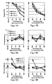
- the response S of a trial is in Fig. 5 shown in a diagram indicating the percent response S as a function of the radiation power and the wavelength of the light irradiation.
- the radiation power of the light irradiation is plotted logarithmically on the X-axis.
- a good response S of more than 90% on the partial sensors is already effected at a very low radiation power (from about 0.5 mW / cm 2 ), which is an activation of the partial sensors equivalent.
- significantly higher radiant power is needed to activate the sub-sensors.
- the light irradiation of the chip 2 is preferably carried out with light of a wavelength of 320 nm to 400 nm.
- Figures 6A and 6B show in diagrams the measured dependence of the nanofibers' electrical resistance in MOhm on the wavelength of the light irradiation, as well as the temperature and the density of the nanofibers.
- Fig. 6A shows the dependence of the electrical resistance on the wavelength of the light irradiation and the operating temperature in a gas sensor with a substantially contiguous layer of nanofibers with a relatively high density (surface coverage between 20 to 30%).
- Fig. 6B Fig. 2 is a graph showing the dependence of the resistance of the nanofiber layer on the wavelength of the irradiation light and the operating temperature for a layer of nanofibers with a low density, namely with less than 10% surface coverage.
- the diagrams show that the resistance depends significantly on the irradiation wavelength.
- the resistance of the nanofibers when irradiated with light of a wavelength of 365 nm is significantly lower than when irradiated with light of a wavelength of 460 nm.
- the resistance in light irradiation with light of a wavelength of 415 nm is between four and ten times higher than the resistance when irradiated with a light wavelength of 365 nm. Therefore, the gas sensor preferably has a light source for UV light having a wavelength below 400 nm.
- Heating of the gas sensor results in a further minimization of the electrical resistance below one MOhm when heated above 100 ° C. and irradiation with light of a wavelength of 365 nm (cf. Fig. 6A ).
- the layers of higher density nanofibers have one lower electrical resistance than those with a low density of nanofibers (see. Fig. 6A With Fig. 6B ).
- the electrical resistances at room temperature were in the experiment above the measuring limit of 340 MOhm, at 50 ° C between 240 MOhm and 340 MOhm and at 100 ° C stable at about 180 MOhm. These electrical resistances refer to the resistors without light irradiation. Under light irradiation, the electrical resistances are significantly reduced.
- the sensitivity of the sensor, the response S increases with decreasing temperature and increasing light energy.
- FIGS. 7A and 7B in each case the sensitivity "Response S" plotted as a percentage as a function of the wavelength of the light irradiation and the temperature of the nanofibers.
- the diagram shows in Fig. 7A the dependence of response S on a layer of nanofibers with high density compared to that in Fig. 7B shown diagram for a layer of nanofibers of lower density.
- the response S is greater for a higher density layer ( Fig. 7A ).
- Fig. 7B The dependence of the sensitivity of the gas sensor on the operating temperature shown is almost negligible for gas sensors with a low density of the layer of nanofibers.
- Such gas sensors or partial sensors of the gas sensor with such a low density work at room temperature almost as well as in the heated state at eg 100 ° C.
- Layers of nanofibers with a relatively high density can consist of hundreds of nanofibers which interconnect the electrodes at the sub-sensors over several hundred microns.
- Layers of nanofibers of relatively low density consist of fewer nanofibers, in which the contact between the electrodes for measuring the electrical resistance of the gas-sensitive material can be produced by a few isolated nanofibers.
- the response S ie the sensitivity of the sensor
- the sensitivity Response S in UV light can be greater than 99% for sub-sensors with layers of nanofibers of a high density, while even at room temperature even at low film densities under UV light irradiation a response S of over 95% can be achieved.
- FIGs 8A and 8B show in each case a diagram of the dependence of the T90 response time on the wavelength of the light irradiation and the temperature of the nanofibers, once for high densities (see Fig. 8A ) and once for low densities (see Fig. 8B ).
- the T90 response time is defined as the time required for the gas sensor to drop in resistance from the output resistance (without light irradiation) to the minimum resistance (with light irradiation) of 90%.
- the T90 response time is a measure of the activation time of the sensor. This activation time is in the Figs. 8A and 8B shown for different wavelengths of light irradiation.
- FIGS 9A and 9B show in each case a T90 recovery time for different wavelengths.
- a T90 recovery time can be measured at the gas sensor.
- the T90 recovery time is defined as the time it takes for the gas sensitive material to turn off after exposure to light irradiation to reach a first saturation plateau after an initial large increase in electrical resistivity.
- the T90 activation times (cf. Figures 8A and 8B ) are usually between 4 and 10 seconds.
- the T90 recovery times are between 8 and 30 seconds.
- the drop in electrical resistance begins immediately after the light source is switched on, so that the detection of gases is possible after only 2 seconds, independent of the T90 response time.
Landscapes
- Chemical & Material Sciences (AREA)
- Engineering & Computer Science (AREA)
- Nanotechnology (AREA)
- Chemical Kinetics & Catalysis (AREA)
- Electrochemistry (AREA)
- Physics & Mathematics (AREA)
- Health & Medical Sciences (AREA)
- Life Sciences & Earth Sciences (AREA)
- Analytical Chemistry (AREA)
- Biochemistry (AREA)
- General Health & Medical Sciences (AREA)
- General Physics & Mathematics (AREA)
- Immunology (AREA)
- Pathology (AREA)
- Investigating Or Analyzing Materials By The Use Of Fluid Adsorption Or Reactions (AREA)
Applications Claiming Priority (1)
| Application Number | Priority Date | Filing Date | Title |
|---|---|---|---|
| DE102014002077.0A DE102014002077B4 (de) | 2014-02-14 | 2014-02-14 | Gassensor, Verfahren zur Detektion von Gasen und Herstellungsverfahren eines Gassensors |
Publications (1)
| Publication Number | Publication Date |
|---|---|
| EP2908121A1 true EP2908121A1 (fr) | 2015-08-19 |
Family
ID=52472169
Family Applications (1)
| Application Number | Title | Priority Date | Filing Date |
|---|---|---|---|
| EP15000410.9A Withdrawn EP2908121A1 (fr) | 2014-02-14 | 2015-02-11 | Capteur de gaz et procédé destiné à la détection de gaz |
Country Status (2)
| Country | Link |
|---|---|
| EP (1) | EP2908121A1 (fr) |
| DE (1) | DE102014002077B4 (fr) |
Cited By (3)
| Publication number | Priority date | Publication date | Assignee | Title |
|---|---|---|---|---|
| WO2019161195A1 (fr) * | 2018-02-15 | 2019-08-22 | Universities Space Research Association | Capteur de gaz à base de nanomatériaux à entrée unique et à sorties multiples |
| CN113358711A (zh) * | 2020-07-21 | 2021-09-07 | 艾感科技(广东)有限公司 | 一种通过调控光和温度制备气体传感器阵列的方法及装置 |
| CN116626111A (zh) * | 2023-05-18 | 2023-08-22 | 浙江大学温州研究院 | 一种快速降低金属氧化物半导体纳米材料气敏电阻的方法 |
Families Citing this family (3)
| Publication number | Priority date | Publication date | Assignee | Title |
|---|---|---|---|---|
| DE102017206124A1 (de) * | 2017-04-10 | 2018-10-11 | Infineon Technologies Ag | Fluidsensor, Verfahren zum Bereitstellen desselben und Verfahren zum Bestimmen eines Bestandteils eines Fluids |
| WO2022136670A1 (fr) | 2020-12-24 | 2022-06-30 | Philip Morris Products S.A. | Procédé et système pour surveiller un matériau de tabac pour détecter une infestation par des insectes |
| EP4020414A1 (fr) | 2020-12-24 | 2022-06-29 | Philip Morris Products S.A. | Procédé de distribution d'articles de génération d'aérosol au niveau d'un point de vente et distributeur automatique pour la distribution d'articles de génération d'aérosol |
Citations (3)
| Publication number | Priority date | Publication date | Assignee | Title |
|---|---|---|---|---|
| EP0769141A1 (fr) | 1994-07-02 | 1997-04-23 | Forschungszentrum Karlsruhe GmbH | Detecteur pour gaz reducteurs ou oxydants |
| US8434647B2 (en) | 2009-08-08 | 2013-05-07 | Riad Aamar | Device for measuring and dispensing a prescribed amount of liquid |
| WO2013095730A2 (fr) * | 2011-09-19 | 2013-06-27 | University Of Utah Research Foundation | Plateforme multimode pour la détection de composés |
Family Cites Families (5)
| Publication number | Priority date | Publication date | Assignee | Title |
|---|---|---|---|---|
| US8052932B2 (en) * | 2006-12-22 | 2011-11-08 | Research Triangle Institute | Polymer nanofiber-based electronic nose |
| DE102006053890A1 (de) * | 2006-11-14 | 2008-05-21 | Eads Deutschland Gmbh | Kampfstoff-Detektor zur Detektion chemischer Kampfstoffe, Herstellungsverfahren und Verwendung eines Substrats als Kampfstoff-Detektor |
| RU2349542C1 (ru) * | 2007-06-22 | 2009-03-20 | Станислав Викторович Хартов | Наноэлектромеханическая структура (варианты) и способ ее получения (варианты) |
| US8443647B1 (en) * | 2008-10-09 | 2013-05-21 | Southern Illinois University | Analyte multi-sensor for the detection and identification of analyte and a method of using the same |
| KR101291312B1 (ko) * | 2011-02-10 | 2013-07-30 | 충남대학교산학협력단 | 광촉매 함유 다공성 나노섬유를 이용한 가스센서 및 이의 제조방법 |
-
2014
- 2014-02-14 DE DE102014002077.0A patent/DE102014002077B4/de active Active
-
2015
- 2015-02-11 EP EP15000410.9A patent/EP2908121A1/fr not_active Withdrawn
Patent Citations (3)
| Publication number | Priority date | Publication date | Assignee | Title |
|---|---|---|---|---|
| EP0769141A1 (fr) | 1994-07-02 | 1997-04-23 | Forschungszentrum Karlsruhe GmbH | Detecteur pour gaz reducteurs ou oxydants |
| US8434647B2 (en) | 2009-08-08 | 2013-05-07 | Riad Aamar | Device for measuring and dispensing a prescribed amount of liquid |
| WO2013095730A2 (fr) * | 2011-09-19 | 2013-06-27 | University Of Utah Research Foundation | Plateforme multimode pour la détection de composés |
Non-Patent Citations (9)
| Title |
|---|
| AUGUSTIN MARTIN ET AL: "UV assisted room temperature gas recognition with SnO2 nanowires", 14TH IEEE INTERNATIONAL CONFERENCE ON NANOTECHNOLOGY, IEEE, 18 August 2014 (2014-08-18), pages 574 - 577, XP032690961, DOI: 10.1109/NANO.2014.6968060 * |
| BONEX WAKUFWA MWAKIKUNGA ET AL: "Towards an electronic nose based on nano-structured transition metal oxides activated by a tuneable UV light source", 2011 IEEE SENSORS PROCEEDINGS : LIMERICK, IRELAND, 28 - 31 OCTOBER 2011, IEEE, PISCATAWAY, NJ, 28 October 2011 (2011-10-28), pages 1109 - 1112, XP032093591, ISBN: 978-1-4244-9290-9, DOI: 10.1109/ICSENS.2011.6127403 * |
| E. ZAMPETTI ET AL: "Gas sensor based on photoconductive electrospun titania nanofibres operating at room temperature", JOURNAL OF NANOPARTICLE RESEARCH, vol. 15, no. 4, 1 April 2013 (2013-04-01), NL, XP055380681, ISSN: 1388-0764, DOI: 10.1007/s11051-013-1566-9 * |
| E. ZAMPETTI ET AL: "UV Assisted Chemical Sensor Based on Electrospun Titania nanofibers Working at Room Temperature", PROCEDIA ENGINEERING, vol. 47, 9 September 2012 (2012-09-09), pages 912 - 915, XP055183120, ISSN: 1877-7058, DOI: 10.1016/j.proeng.2012.09.295 * |
| J.D. PRADES ET AL: "Equivalence between thermal and room temperature UV light-modulated responses of gas sensors based on individual SnO2 nanowires", SENSORS AND ACTUATORS B: CHEMICAL, vol. 140, no. 2, 21 May 2009 (2009-05-21), pages 337 - 341, XP055183402, ISSN: 0925-4005, DOI: 10.1016/j.snb.2009.04.070 * |
| JIAN GONG ET AL: "UV-Light-Activated ZnO Fibers for Organic Gas Sensing at Room Temperature", JOURNAL OF PHYSICAL CHEMISTRY C, vol. 114, no. 2, 23 December 2009 (2009-12-23), pages 1293 - 1298, XP055183085, ISSN: 1932-7447, DOI: 10.1021/jp906043k * |
| MARTIN AUGUSTIN ET AL: "UV-VIS sensor system based on SnO2 nanowires", SENSORS AND ACTUATORS A: PHYSICAL, vol. 210, 25 February 2014 (2014-02-25), pages 205 - 208, XP055183391, ISSN: 0924-4247, DOI: 10.1016/j.sna.2014.02.016 * |
| R. WIERZBICKI ET AL: "Black silicon maskless templates for carbon nanotube forests", MICROELECTRONIC ENGINEERING, vol. 104, 8 December 2012 (2012-12-08), pages 110 - 113, XP055183398, ISSN: 0167-9317, DOI: 10.1016/j.mee.2012.11.019 * |
| SUNGHOON PARK ET AL: "UV-Enhanced NO 2 Gas Sensing Properties of SnO 2 -Core/ZnO-Shell Nanowires at Room Temperature", ACS APPL.MATER.INTERFACES, vol. 5, no. 10, 22 May 2013 (2013-05-22), pages 4285 - 4292, XP055380693, ISSN: 1944-8244, DOI: 10.1021/am400500a * |
Cited By (3)
| Publication number | Priority date | Publication date | Assignee | Title |
|---|---|---|---|---|
| WO2019161195A1 (fr) * | 2018-02-15 | 2019-08-22 | Universities Space Research Association | Capteur de gaz à base de nanomatériaux à entrée unique et à sorties multiples |
| CN113358711A (zh) * | 2020-07-21 | 2021-09-07 | 艾感科技(广东)有限公司 | 一种通过调控光和温度制备气体传感器阵列的方法及装置 |
| CN116626111A (zh) * | 2023-05-18 | 2023-08-22 | 浙江大学温州研究院 | 一种快速降低金属氧化物半导体纳米材料气敏电阻的方法 |
Also Published As
| Publication number | Publication date |
|---|---|
| DE102014002077A1 (de) | 2015-08-20 |
| DE102014002077B4 (de) | 2015-08-27 |
Similar Documents
| Publication | Publication Date | Title |
|---|---|---|
| DE102014002077B4 (de) | Gassensor, Verfahren zur Detektion von Gasen und Herstellungsverfahren eines Gassensors | |
| DE19618935C2 (de) | Gassensor und Verfahren zur Herstellung eines Gassensors | |
| DE19513274C2 (de) | Verfahren zur Messung des Taupunkts oder einer Gaskonzentration und Einrichtung zur Vorhersage einer Vereisung | |
| AT508976B1 (de) | Feuchtigkeitssensor | |
| DE2428884A1 (de) | Absorptionsspektrographisches analyseverfahren und einrichtung zu seiner durchfuehrung | |
| EP1517132A1 (fr) | Mesure sans contact de la température de la surface d'un échantillon exposé aux intempéries artificielles ou naturelles | |
| EP0046989B1 (fr) | Capteur de gaz sélectif en couches minces de hautes sensibilité et stabilité pour la détection et la mesure d'impuretés gazeuses organiques dans l'air à base d'oxyde semi-conducteur de tungstène, ainsi que son procédé de fabrication | |
| DE102018122860A1 (de) | Verfahren zum Betreiben einer Sensorvorrichtung | |
| EP1635164B1 (fr) | Méthode pour calibrage d'un système de mesure de photoluminescence | |
| EP0859536B1 (fr) | Radiateur infra-rouge et son application | |
| DE2521366C2 (de) | Sonde zum selektiven Detektieren mindestens eines Bestandteils mit polaren Molekülen eines gasförmigen Gemisches | |
| EP2820448A1 (fr) | Procédé de détection d'un rayonnement et dispositif d'analyse permettant d'analyser un échantillon en mettant en uvre un rayonnement. | |
| DE112016000301T5 (de) | NOx-Sensor | |
| DE102010003056B4 (de) | Verfahren zur Erzeugung von Bildern einer Probe | |
| EP3717893B1 (fr) | Procédé et dispositif pour déterminer la conductivité électrique | |
| DE2832828A1 (de) | Kohlenstoff-monoxyd-detektor | |
| DE102021100756A1 (de) | Verfahren und Anordnung zur Beobachtung von Flammen in einem Heizgerät, das mit Wasserstoff oder wasserstoffhaltigem Brenngas betreibbar ist | |
| DE102021213046B3 (de) | Sensor, Sensorsystem und Verfahren zur Erfassung thermodynamischer Kenngrößen einer Probe sowie die Verwendung des Sensors oder Sensorsystems | |
| DE102016215881A1 (de) | Verfahren zur Durchführung eines Erholungsprozesses von Gassensoren | |
| DE102008048342B4 (de) | SERS-Substrat, Verfahren zu seiner Herstellung und Verfahren zum Detektieren eines Analyten mittels SERS | |
| DE102007043470B4 (de) | Vorrichtung zur langzeitstabilen Strahlungsmessung und Verfahren zu deren Funktionsprüfung | |
| EP0869353B1 (fr) | Procédé de fabrication d'un capteur | |
| EP0627621B1 (fr) | Méthode et appareil pour l'examen du métabolisme dans des cellules | |
| DE102016206445B4 (de) | Coulometrischer Feuchtesensor mit gelförmigem Elektrolyt und Herstellungsverfahren für einen Coulometrischen Feuchtesensor mit gelförmigem Elektrolyt | |
| DE102022123559B3 (de) | Verfahren und Vorrichtung zur Performanzüberwachung und -regelung einer Ionenquelle |
Legal Events
| Date | Code | Title | Description |
|---|---|---|---|
| PUAI | Public reference made under article 153(3) epc to a published international application that has entered the european phase |
Free format text: ORIGINAL CODE: 0009012 |
|
| AK | Designated contracting states |
Kind code of ref document: A1 Designated state(s): AL AT BE BG CH CY CZ DE DK EE ES FI FR GB GR HR HU IE IS IT LI LT LU LV MC MK MT NL NO PL PT RO RS SE SI SK SM TR |
|
| AX | Request for extension of the european patent |
Extension state: BA ME |
|
| 17P | Request for examination filed |
Effective date: 20160211 |
|
| RBV | Designated contracting states (corrected) |
Designated state(s): AL AT BE BG CH CY CZ DE DK EE ES FI FR GB GR HR HU IE IS IT LI LT LU LV MC MK MT NL NO PL PT RO RS SE SI SK SM TR |
|
| 17Q | First examination report despatched |
Effective date: 20170622 |
|
| STAA | Information on the status of an ep patent application or granted ep patent |
Free format text: STATUS: THE APPLICATION HAS BEEN WITHDRAWN |
|
| 18W | Application withdrawn |
Effective date: 20171219 |